

Page 1
Any and all SANYO products described or contained herein do not have specifications that can handle
applications that require extremely high levels of reliability, such as life-support systems, aircraft’s
control systems, or other applications whose failure can be reasonably expected to result in serious
physical and/or material damage. Consult with your SANYO representative nearest you before using
any SANYO products described or contained herein in such applications.
SANYO assumes no responsibility for equipment failures that result from using products at values that
exceed, even momentarily, rated values (such as maximum ratings, operating condition ranges,or other
parameters) listed in products specifications of any and all SANYO products described or contained
herein.
CMOS IC
Single-Chip 4-bit Microcontroller
(Low-Threshold Input, On-Chip FLT Driver)
Ordering number:ENN1802C
LC6514B
SANYO Electric Co.,Ltd. Semiconductor Company
TOKYO OFFICE Tokyo Bldg., 1-10, 1 Chome, Ueno, Taito-ku, TOKYO, 110-8534 JAPAN
Overview
The LC6514B is a microcontroller with FLT drivers. It is
identical with the LC6510C in the internal architecture and
instruction set. Since the normal/low-threshold lev el of input port A can be selected by option and the on-chip pulldown resistor can be bitwise connected to the FLT driver
by option, the number of external parts used in the user
equipment can be minimized, reducing the cost consider-
ably.
Features
• Low power dissipation.
• ROM capacity : 4096×8 bits.
• RAM capacity : 256×4 bits.
• Subroutine stack : 8 levels (common with interrupt).
• On-chip OSC circuit
CR OSC : 800kHz typ.
Ceramic OSC : 400kHz, 800kHz, 1000kHz
External iuput : 1290kHz max.
• Power-down by 2 standby modes
HAL T mode : Po wer dissipation sa ving by program stadby
during normal operation
HOLD mode : Power supply backup during power fail-
ure.
• Input/output ports
Input : 4 bits × 1 port
3 bits × 1 port
Input/output : 4 bits × 2 ports
Output : 4 bits × 4 ports
2 bits × 1 port
• Interrupt.
External interrupt : 1
Internal timer interrupt : 1
• On-chip 4-bit prescaler and 8-bit program timer.
• Instruction cycle time : 3.1µs (at 1290kHz)
• Supply voltage
Normal operation : 4.0 to 6.0 V
Memory hold : 1.8 to 6.0 V
• Instruction set common to the LC6502, LC6505 (BANK
instruction added)
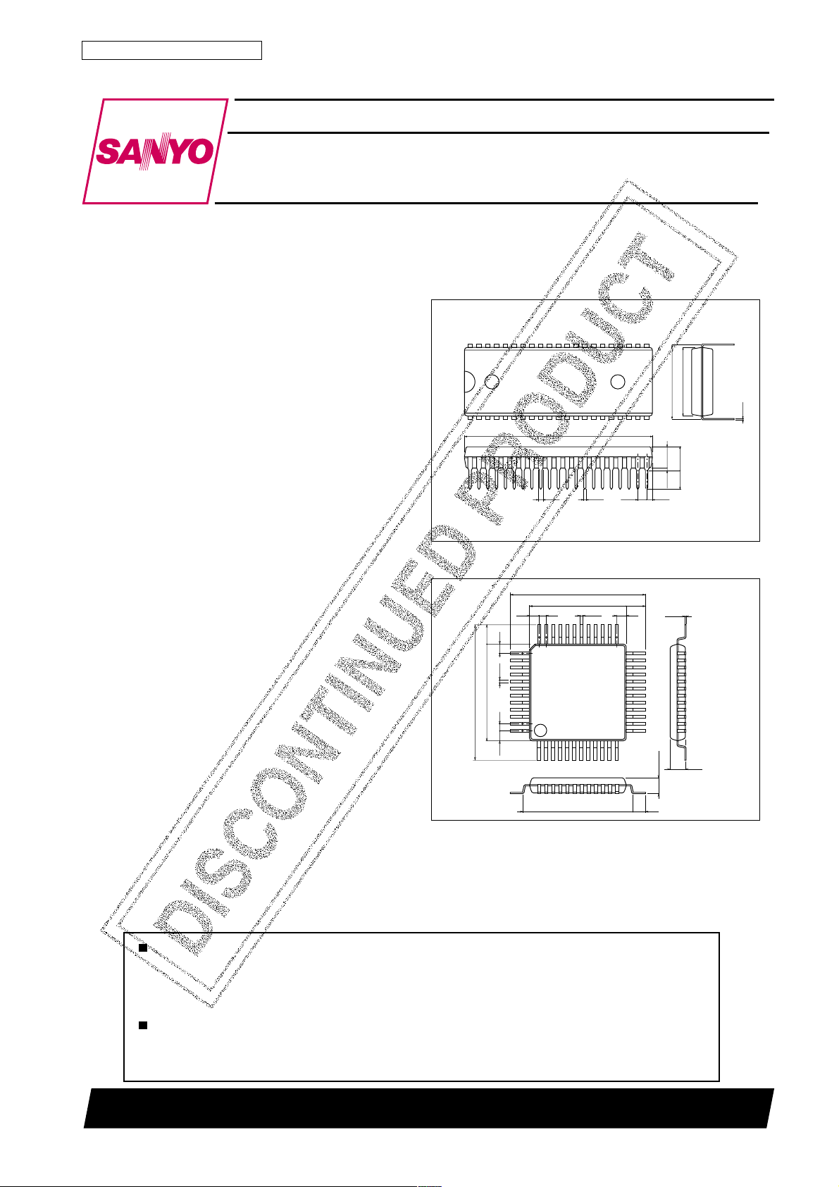
Package Dimensions
unit:mm
3025B-DIP42S
[LC6514B]
42
1
unit:mm
3052B-QIP48
3.0
1.5
0.35
20.0
14.0
1.0
1.5
37.9
20.0
14.0
0.48
0.35
16.6
0.95
1.5
1.0
36
37
48
1
22
13.8
15.24
21
4.25
5.1max
3.8
1.15
3.0
1.5
24
13
2.45max
1.7
0.51min
SANYO : DIP42S
0.15
2.15
SANYO : QIP48A
1.78
25
12
0.25
O1501TN (KT)/7209YT/3246KI/2265KI, TS No.1802–1/17
Page 2
LC6514B
Note
The LC6514B heretofore in use has been improved by changing the value of the pull-down resistor to be contained in
FLT drivers as shown below. When using the LC6514B, fully check that the new resistor value meets your application
specifications.
tnerructuptuolevel-L
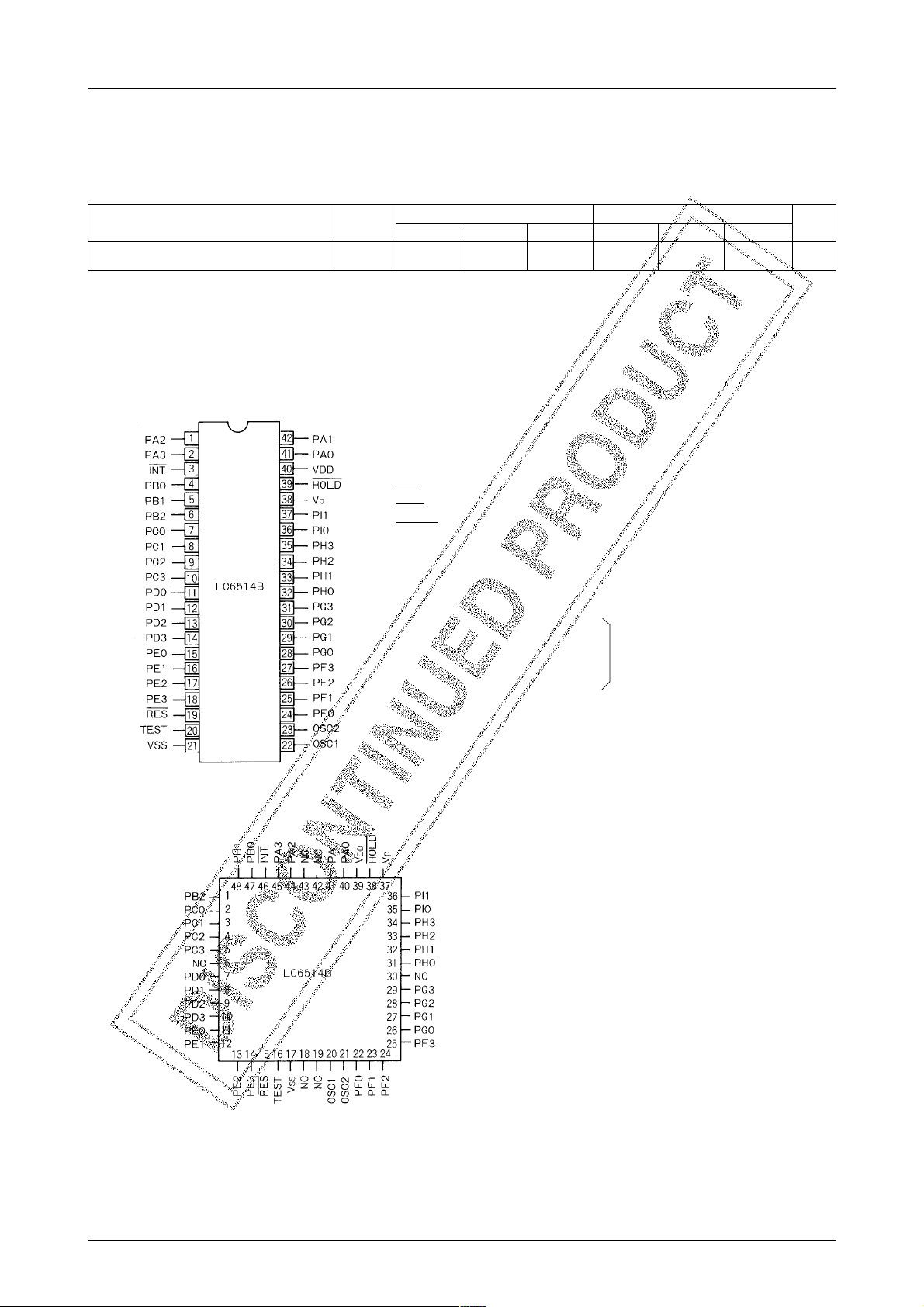
Pin Assignment
retemaraP
I
)ecnatsisernwod-lluptuptuO(
R(DP)
LO
nimpytxamnimpytxam
091.0
)002(
eulavrotsiserweNeulavrotsiserdlO
263.0
)501(
067.0
)05(
tinU
801.0
)053(
403.0
)521(
345.0
Am
)07(
k( Ω)
Pin name
OSC1, OSC2 : C, R or ceramic resonator for system OSC
INT : Interrupt
RES : Reset
HOLD :Hold
PA
PB
PC
PD
PE
PF
PG
PH
PI
: Input port A
0 to 3
: Input port B
0 to 2
: Input/output common port C
0 to 3
: Input/output common port D
0 to 3
: Output port E
0 to 3
: Output port F
0 to 3
: Output port G
0 to 3
: Output port H
0 to 3
: Output port I
0, 1
0 to 3
0 to 2
0 to 3
0 to 3
0 to 3
0 to 3
0, 1
0 to 3
0 to 3
With
High-voltage
driver
TEST : TEST
V
: Power supply for high-voltage port pull-down resistor
p
When mounting the QIP package
version on the board, do not dip it in
solder.
NC pin : No connection
No.1802–2/17
Page 3

Pin Function
emaNniP
TNItupnI.niptupnitseuqertpurretnI
DLOHtupnI
SERtupnI.niptupniteseR
AP
3ot0
BP
2ot0
CP
3ot0
DP
3ot0
EP
3ot0
FP
3ot0
GP
3ot0
HP
3ot0
IP
1,0
1CSOtupnI
2CSOtuptuO .edomkcolclanretniehtroftiucricecnanoseragnitcennocyllanretxerofniP
V
DD
V
SS
PVtupnI.rotsisernwod-lluptropegatlov-hgihrofylppusrewoP
TSETtupnI
– .ylppusrewopV0otdetcennoC
LC6514B
/tupnI
tuptuO
AtroptupnI
Aot
0
3
tupnI
BtroptupnI
Bot
0
tupnI
/tupnI
tuptuO
/tupnI
tuptuO
tuptuO
tuptuO
tuptuO
tuptuO
tuptuO
tupnI
2
Ctropnommoctuptuo/tupnI
Dtropnommoctuptuo/tupnI
EtroptuptuO
Eot
0
3
FtroptuptuO
Fot
0
3
GtroptuptuO
Got
0
3
HtroptuptuO
Hot
0
3
ItroptuptuO
0I,1
.nipylppusrewoP
.niptsetCI
VdetcennocyllamroN
SS
.)egatlovlamroN(
.)egatlovlamroN(
Cot
0
3
Dot
0
3
.kcolclanretxegniylppusrofniP
.V5+otdetcennocyllamroN
.)V0(
.hcnarbrofnoisicedtib-elgnisdnatupnitib-4foelbapaC
.tupnitseuqeresaeleredomTLAHrofosladesU
.noitpoybelbatcelesstib4roftupnidlohserhtWOL
.hcnarbrofnoisicedtib-elgnisdnatupnitib-3foelbapaC
.)egatlovlamroN(
.)egatlovlamroN(
.)revirdtnemgesegatlov-hgihhtiw(
.teser/testib-elgnisdnatuptuotib-4foelbapaC
.)revirdtnemgesegatlov-hgihhtiw(
.teser/testib-elgnisdnatuptuotib-4foelbapaC
.)revirdtigidegatlov-hgihhtiw(
.teser/testib-elgnisdnatuptuotib-4foelbapaC
.)revirdtigidegatlov-hgihhtiw(
.teser/testib-elgnisdnatuptuotib-4foelbapaC
.)revirdtigidegatlov-hgihhtiw(
.teser/testib-elgnisdnatuptuotib-2foelbapaC
noitcnuF
).noitcnufni50/2056CLehtmorfsreffiD(niptupnitseuqeredomDLOH
.desusiedomybdnatsehtsselnutroptupnitib-elgnisesoprup-larenegsadesugniebfoelbapaC
.tupnignirudhcnarbrofnoisicedtib-elgnisdnatupnitib-4foelbapaC
.tuptuognirudteser/testib-elgnisdnatuptuotib-4foelbapaC
.tupnignirudhcnarbrofnoisicedtib-elgnisdnatupnitib-4foelbapaC
.tuptuognirudteser/testib-elgnisdnatuptuotib-4foelbapaC
.hcnarbrofhctaltuptuofonoisicedtib-elgnisdnastnetnochctaltuptuofotupnitib-4foelbapaC
.noitpoybelbatcelesesiwtibrotsisernwod-llupfoesunon/esU
.hcnarbrofhctaltuptuofonoisicedtib-elgnisdnastnetnochctaltuptuofotupnitib-4foelbapaC
.noitpoybelbatcelesesiwtibrotsisernwod-llupfoesunon/esU
.hcnarbrofhctaltuptuofonoisicedtib-elgnisdnastnetnochctaltuptuofotupnitib-4foelbapaC
.noitpoybelbatcelesesiwtibrotsisernwod-llupfoesunon/esU
.hcnarbrofhctaltuptuofonoisicedtib-elgnisdnastnetnochctaltuptuofotupnitib-4foelbapaC
.noitpoybelbatcelesesiwtibrotsisernwod-llupfoesunon/esU
.hcnarbrofhctaltuptuofonoisicedtib-elgnisdnastnetnochctaltuptuofotupnitib-2foelbapaC
.noitpoybelbatcelesesiwtibrotsisernwod-llupfoesunon/esU
.2CSOnipdnanipsihtotdetcennocsirotanosercimarecaroR,C,desusiedomkcolclanretniehtfI
No.1802–3/17
Page 4
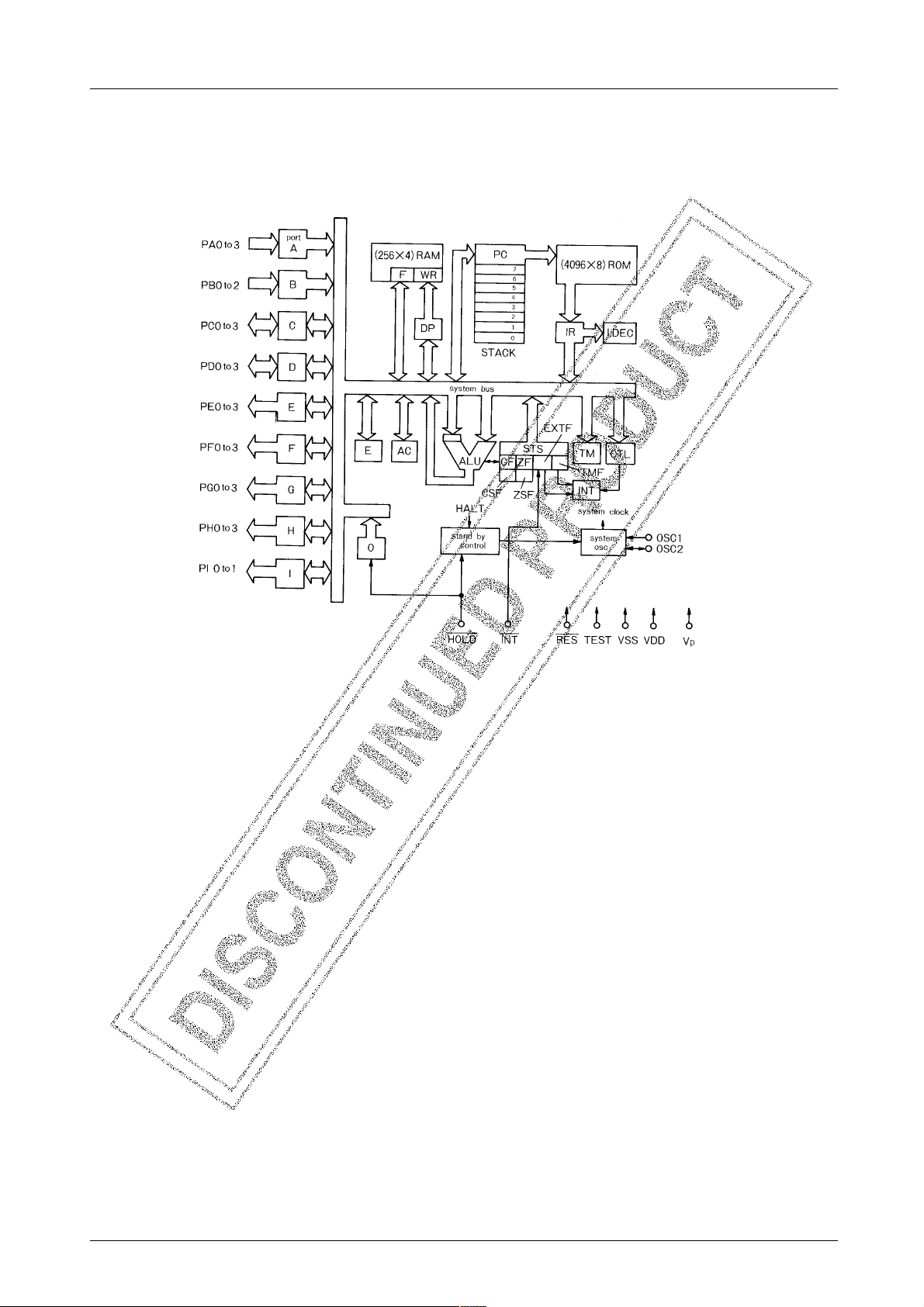
System Block Diagram
LC6514B
RAM : Data memory ROM : Program memory
F : Flag PC : Program counter
WR : Working register INT : Interrupt control
AC : Accumulator IR : Instruction resister
ALU : Arithmetic and logic unit I.DEC : Instruction decoder
DP : Data pointer CF, CSF : Carry flag
E : E register Carry save flag
CTL : Control register ZF, ZSF : Zero flag
OSC : Oscillator Zero save flag
TM : Timer EXTF : External interrupt request flag
STS : Status register TMF : Internal interrupt request flag
No.1802–4/17
Page 5

LC6514B
Absolute Maximum Ratings at Ta = 25˚C, VSS=0V (VDD=5V±20% unless otherwise specified)
retemaraPlobmySsnoitidnoCsgnitaRtinU
egatlovylppusmumixaMV
egatlovtupnI
egatlovtuptuO
tnerructuptuokaeP
noitapossidrewopelbawollA
erutarepmetgnitarepOrpoT 07+ot03–°C
erutarepmetegarotSgtsT 521+ot55–°C
Note 1: For pin OSC1, up to oscillation amplitude generated when internaly oscillated under the recommended
oscillation conditions in Fig. 3 is allowable.
xam 0.7+ot3.0– V
DD
V
1NI
V
V
V
I
I
I
I
V
2NI
P
1TUO
2TUO
1O
2O
3O
4O
1xamdP07+ot03–=aT,egakcappiD °C006Wm
2xamdP07+ot03–=aT,egakcaptalF °C004Wm
I,H,G,F,EstroPV
)1etoN(pVnahtrehtostupnIot3.0– V
V
I,H,G,F,EstropnahtrehtostuptuOot3.0– V
D,CstropfoniphcaE 0.2+ot0.2– Am
F,EstropfoniphcaE 0ot01– Am
I,H,GstropfoniphcaE 0ot51– Am
IotCstropfosnipllA 61+ot09– Am
ot54– V
DD
ot54– V
DD
DD
DD
DD
DD
3.0+V
3.0+V
3.0+V
3.0+V
Recommended Operating Conditions at T a = –30˚C to +70˚C, V
specified)
retemaraPlobmySsnoitidnoC
egatlovylppusgnitarepOV
egatlovylppusnwod-rewoPV
egatovtupnilevel-H
egatovtupnilevel-L
ycneuqerfkcolcgnitarepOf
htdiweslupkcolclevel-Ht
htdiweslupkcolclevel-Lt
emitesirtupnikcolCt
emitllaftupnikcolCt
CSORCrofecnaticapaclanretxEtxeC
CSORCrofecnatsiserlanretxEtxeR
CSOcimarecrofstnatsnoctiucriclanretxE
gnimitybdnatS
niyaledelbawollAt
tiucricnacsyeKt
DD
RM=DLOHV
DD
V
1HI
V
V
V
V
V
V
wφH
t
t
V
2HI
3HI
1LI
V
2LI
3LI
V
4LI
csotxe
wφL
R 2.0sµ
cso
F 2.0sµ
cso
2R,1R
2C,1C
RDDV
FDDV
LD
HD
4LI
DD
DD
DD
8.giFeeS
3.giFeeS
V,6.giFeeS
DD
.01,9.giFeeS
edomDLOH,8.10.6V
snip1CSO,SER,TNIV
= 0V(VDD = 4.0V to 6.0V unless otherwise
SS
gnitaR
nimpytxam
0.40.50.6V
"tupnidlohserhtlamron":Atrop,DotAstroP
"tupnidlohserhtwol":Atrop,V5.5ot5.4=9.1V
snip1CSO,DLOH,SER,TNI
"tupnidlohserhtlamron":Atrop,DotAstroPV
"tupnidlohserhtwol":Atrop,V5.5ot5.4=V
snipTSET,DLOH,V0.6ot8.1=V
1.giFeeS,tupnikcolclanretxetA
V0.6ot8.1=
V7.0
DD
V8.0
DD
SS
SS
SS
SS
2220921zHk
3.0sµ
3.0sµ
0sµ
0sµ
V
V
V3.0
V2.0
V2.0
tinU
V
DD
V
DD
V
DD
V
DD
5.0V
V
DD
V
DD
%5±022
Fp
%1±8.6
kΩ
cT·)3-n(
sµ
cT·)3-n(
sµ
No.1802–5/17
Page 6
LC6514B
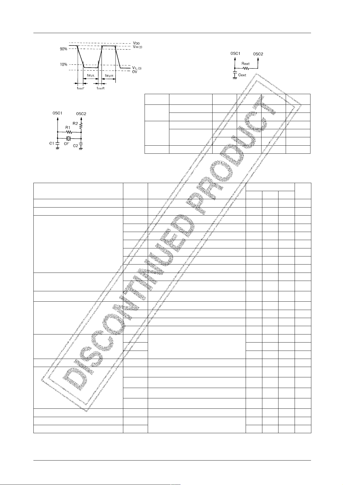
Fig. 2 Recommended Oscillator for CR OSC
Fig. 1 OSC1 Pin input waveform
CF : Ceramic resonator
CSB400P (Murata)
KBR400B (Kyocera)
CSB800K (Murata)
KBR800H (Kyocera)
CSB1000K (Murata)
Fig. 3 Recommended Oscillator for Ceramic OSC
retneC
ycneuqerF
zHk004
zHk008
zHk0001)ataruM(K0001BSC00100100015.1
FC)Fp(1C)Fp(2Ck(1R Ω)k(2R Ω)
)ataruM(P004BSC07407400015.1
)arecoyK(B004RBK07407400015.1
)ataruM(K008BSC02202200010.1
)arecoyK(H008RBK
C1, C2 : Tolerance ±10%
R1, R2 : Tolerance ±5%
Electrical Characteristics at Ta = –30 to +70˚C, VDD=5V±20%, VSS=0V
retemaraPlobmySsnoitidnoC
(Note 1) f
tnerructupuilevel-HI
tnerructupuilevel-LI
egatovtuptuolevel-H
egatovtuptuolevel-L
tnerructuptuoevel-L
)rotsisernwod-lluptuptuO(
tnerruckaelFFOtuptuO
CSOcimarecrofycneuqerfCSOkcolC
CSORCrofycneuqerfCSOkcolCf
niardtnerruC
ecnaticapactupnIC
ecnaticapactuptuOC
ecnaticapactuptuo/tupnIC
: Oscillatable frequency.
CFOSC
f
f
f
V
V
V
V
V
V
V
V
V
I
R(DP)
I
I
I
I
I
I
I
I
HI
LI
1HO
2HO
3HO
4HO
5HO
6HO
7HO
1LO
2LO
LO
1FFO
2FFO
3FFO
4FFO
1CSOFC
2CSOFC
3CSOFC
C
CSORC
txe
1DD
2DD
3DD
4DD
NI
TUO
OI
V,nip
NIV=DD
4
5
zHM1=f5Fp
VtpecxesniptupnillA
PV,NIV=DD
VtpecxesniptupnillA
PV,NIV=SS
I:D,CstroP
Am1–=
HO
I:D,CstroP
I:F,EstroP
I:F,EstroP
I:D,CstroP
LO
V:D,CstroP
V:D,CstroP
V:IotEstroP
V:IotEstroP
R,Fp022=
C,CSORCtA
V,edomTLAH
V,edomDLOH
Aµ001–=
HO
Am2–=
HO
HO
I:I,H,GstroP
I:I,H,GstroP
I:I,H,GstroP
Am01–=
HO
Am2–=
HO
HO
Am1=4.0V
V:I,H,G,F,EstroP
P
rotsisernwod-lluphtiw,nepo
txe
V,niptupni,nepo
DD
DD
V:I,H,G,F,EstroP
V=
TUO
V=
TUO
TUO
TUO
txe
NIV=DD
V,V53–=
P
rotsisernwod-lluphtiw
DD
SS
V=
DD
V=
DD
)1etoN(3.giFnitiucric
k8.6= Ω 2.giFnitiucricCSOta,0060080221zHk
R,Fp022=
txe
02202200010.1
05105100015.1
gnitaR
nimpytxam
1– Aµ
VDD0.2–
VDD5.0–
VDD0.1–
Istroplla,Am1–=
ecnadepmihgih:tuptuo,zHM1=f
Am1–=
HO
Istroplla,Am1–=
HO
V,V3=
LO
DD
tuptuoDO,03Aµ
tuptuoDO,V04– 03– Aµ
k8.6= Ω niptuptuo,
VDD5.0–
VDD8.1–
VDD0.1–
VDD5.0–
Am1–=
tuptuo,FFOrTtuptuo,V53–=
,V5=
CSOta,CSOcimarecrofsnoitidnocdednemmoceR
tupni,neponiptuptuo,)zHk008(CSOcimarectA
.giFnitiucrictsetta,V0.6ot0.4=
091.0
)002(
0.1– Aµ
483004614zHk
867008238zHk
06900010401zHk
.giFnitiucrictsetta,V0.6ot8.1=
263.0
)501(
0.10.2Am
0.10.2Am
01Fp
01Fp
1Aµ
33– V
067.0
)02(
0.1Aµ
01Aµ
01Aµ
V
V
V
V
V
V
V
k( Ω)
tinU
Am
No.1802–6/17
Page 7

Fig. 4 I
Test Circuit
DD3
LC6514B
Input/output common
port C, D : Output inhibit
The HALT instruction is
executed to csuse the
HALT mode to be
entered.
Fig. 5 I
Test Circuit
DD4
Fig. 6 Standby Mode Timing
(Note)
During the HALT instruction
execution cycle, no chattering
must be applied to the HOLD
pin and PA
0 to 3
pins.
No.1802–7/17
Page 8

LC6514B
τV
: Power supply rise time constant
DD
τRES : RES pin rise time constant
Fix C, R so that τV
yielded. (t
: OSC stabilized time)
OSC
≤τRES,t
DD
OSC
≥10ms is
Fig. 7 Initial Reset Timing
CR OSC characteristic of LC6514B
Fig. 8 shows the CR OSC characteristic of the LC6514B. For the variation range of CR OSC frequency of the
LC6514B, the following is guaranteed at external consatants of Cext=220pF, Rext=6.8kΩ only. The outgoing inspection is performed under this condition only.
Ta=–30°C to +70°C
600kHz≤f
If any other constants than specified above are used, the range of Rext=5k to 50kΩ, Cext=100p to 300pF must be
observed. (See Fig. 8.)
Fig. 8 f
CROSC.
CROSC
–Rext
≤1220kHz
(
VDD=4 to 6V
)
Note 1. The OSC frequency at VDD=5V, Ta=25°C
must be 800KHz or less.
Note 2. The OSC frequency at V
Ta=–30 to +70°C must be within the
operation clock frequency range
(222KHz to 1290 kHz).
=4 to 6V,
DD
No.1802–8/17
Page 9

LC6514B
Proper Cares in using the IC
[Digit drive signal-used key scan]
When key-scanning with the FLT digit drive signal in Fig. 9 and inputting the return signal to port A, the following
must be observed.
(a) Estimate voltage drop (V
teristic of the output port of the LC6514B.
(b) Estimate voltage drop (V
(c) Check to see that (V
ON
) in the output transistor using the current flowing in an FLT used and the V-1 charac-
ON
) in the switch circuit.
SW
+ VSW) meets the VIH/VIL requirement of the input port.
Fig. 9 Sample Key Scan Application
For the key scan application in Fig. 9, make the program considering the deley in the external circuit and the input
delay shown below.
N : Number of instruction cycles existing between instruction (OP, SPB, RPB) used to output data to output port and
insutruction (IP, BP, BNP) used to input data from input port. (Number of instruction cycles to be programmed
according to the length of t
, tDH : Delay in external circuit from output port to input port.
t
DL
DL
, tDH)
When the IP instruction is used to input the return signal as shown in Fig. 10, the input delay must be considered and
three instructions are placed between the IP instruction and the crossing of input port waveform and V
or V
VI
H1
Some instructions must be placed additionally according to the length of delay (t
respectively.
IH2,
, tDH) in the external circuit after
DL
IL1
or V
IL2
,
the digit drive signal is delivered with the execution of the OP instruction ( a and c ).
No.1802–9/17
Page 10

LC6514B
<Notes for Standby Fuction Application>
[Proper cares in using standby function]
The LC6514B provides the standby function called HALT, HOLD mode to minimize the current drain when the
program is in the wait state. The standby function is controlled by the HALT instruction, the HOLD pin, RES pin. A
peripheral circuit and program must be so designed as to provide precise control of the standby function. In most
applications where the standby function is performed, voltage regulation, instantaneous break of power, and external
noise are not negligible. When designing an application circuit and program, whether or not to take some measures
must be considered according to the extent to which these factors are allowed.
This section mainly describes power failure backup for which the satndby function is mostly used. A sample application circuit where the standby function is performed precisely is shown below and notes for circuit design and program design are also given below. When using the standby function, the application circuit shown below must be used
and the notes must be also fully observed. If any other method than shown in this section is applied, it is necessary to
fully check the environmental conditions such as power failure and the actual operation of an application equipment.
[Sample application and notes]
When using the HOLD mode, an appliacation circuit and program must be designed with the following in mind.
(1) The supply voltage at the standby state must not be less than specified.
(2) Input timing of each control signal (HOLD, RES port A, INT, etc.) at the standby initiate/release state.
(3) Release operation must not be overlapped at the time of execution of the HALT instruction.
A sample application where the standby function is used for power failure backup is shown below as a concrete
method to observe these notes. A sample application circuit, its operation, and notes for program design are given
below.
1. Sample application where the standby function is used for power failure backup.
Power failure backup is an application where power failure of the main power source is detected by the HOLD pin,
etc. to cause the HOLD mode to be entered so that the current drain is minimized and a backup capacitor is used to
retain the contents of the internal registers even during power failure.
1-1. Sample application circuit (CF OSC)
Fig. 11 shows a CF OSC-applied circuit where the standby function is used for power failure backup.
Unit (resistance : Ω, capacitance : F)
Fig. 11 Sample Application Circuit
No.1802–10/17
Page 11

LC6514B
1-2. Operating waveform
The operating waveform in the sample application circuit in Fig. 11 is shown below. The mode is roughly divided
as follows.
1 Initial application of power
2 Instantaneous break
3 Return from backup mode
1-3. Operation of sample application circuit
1 At the time of initial application of power
A reset occurs and the execution of the program starts at address 000H of the program counter (PC).
2 At the time of instantaneous break
(1) At the time of very short instantaneous break
The execution of the program continues.
(2) At the time of instantaneous break being a little longer than (1)
(When the RES input voltage meets V
and HOLD input voltage does not meet VIL)
IL
A reset occurs during the execution of the program and the execution of the program starts at address 000H of
the program counter (PC).
Since the HOLD request signal is not applied to the HOLD pin, the HOLD mode is not entered.
(3) At the time of long instantaneous break (When both of the RES input voltage and HOLD input voltage meet
)
V
IL
The HOLD request signal is applied to the HOLD pin and the HOLD mode is entered.
When V+ rises after instantaneous break, a reset occurs to release the HOLD mode and the execution of the
program starts at address 000H of the program counter (PC).
3 At the time of return from backup voltage
A reset occurs and the execution of the program starts at address 000H of the program counter (PC).
No.1802–11/17
Page 12

LC6514B
1-4. Notes for circuit design
1 How to fix C3, R6, C2, R2
Fix closed loop A dischar ge time constants C3, R6 and HOLD pin char ge time constants C2, R2 so that closed loop
A fully discharges before the HOLD input voltage gets lo wer than V
input voltage is sure to get lower than V
input voltage gets lower than V
.
IL
(a reset occurs) when V+ rises after instantaneous break where the HOLD
IL
2 How to fix C3, R7
Fix RES pin charge time constats C3, R7 so that when power is applied initially or the HOLD mode is released the CF
OSC oscillates normally and the RES input voltage exceeds V
IH
3 How to fix R4, R5
Fix Tr bias constants R4, R5 so that when V+ rises after instantaneous break the RES input voltage gets lower than
(brought to L-level) befor the HOLD input voltage exceeds V
V
IL
4 How to fix C2, R3
Fix HOLD pin charge time constants C2, R3 so that when the HOLD mode is released from the backup mode the
HOLD input voltage does not exceed V
(brought to L-level).
V
IL
(not brought to H-level) until the RES input voltage gets lower than
IH
Fix C3, R7 and C2, R3 so that the time interval from the moment the HOLD input voltage exceeds V
input voltage exceeds V
is longer than the CF OSC stabilizing time.
IH
5 When the load is heavy or the polling interval is long
Since C1 discharges largely, increase the capacity of C1 or separate B detection from V+ and use a power supply or
signal that rises faster than V+.
at the time of instantaneous break and the RES
IL
and the program starts running.
(brought to H-level).
IH
until the RES
IH
1-5. Notes for software design
When the HOLD request signal is detected, the HALT instruction is executed immediately. A concrete example is
shown below.
1 An interrupt is inhibited before polling the HOLD request pin (HOLD pin).
2 Polling of the HOLD pin and the HALT instruction are programmed consecutively.
[Concrete example]
RCTL 3 ; EXTEN, TMEN←0 (External, timer interrupt intibit)
BPO AAA ; Polling of the HOLD pin (If H-level, a branch occurs to AAA.)
HALT ; The HOLD mode is entered.
AAA :
No.1802–12/17
Page 13

LC6514B
Application development tools
Evaluation chip (LC6597), simulation chip (LC65PG97) and the dedicated equipment called “applicaction development tools” are available to facilitate application development of the LC6514B.
• SDS-410 system
This is combination of floppy disk-provided CPU, CRT, and priter. This system enables application deveropment
programs of microcomputers to be prepared (edited, assembled) very speedily and efficiently in assembly language. By connecting the EVA-410 to the CPU, programs can be debugged and assembled data can be written into
the EPROM (using EPROM WRITER function contained in the EVA-410).
• EVA-410
This is an evaluation kit having EPROM WRITER function, function of parallel/serial data communication with
external equipment (SDS-410, etc.). This kit enables application development programs to be corrected or debugged
on the machine language level.
• EVA-TB3B
This is board which is connected with the EVA-410 to develop programs dedicated to the LC6514B.
• EVA-97-14B
Simulation chip (LC65PG97) is identical with the LC6510C in the I/O port breakdown voltage and pin assignment.
Since the LC6514B has high-voltage output ports and differs partially in the pin assignment, conversion board
“EVA-97-14B” with high-voltage drivers is used to evaluate the LC6514B.
(Note) The threshold level of input port A of the LC6514B can be selected to be normal/low level by option. However,
since port A of the EVA-TB3B, EVA-97-14B is of normal threshold input type, they cannot be used to evaluate
the low threshold input version of the LC6514B.
No.1802–13/17
Page 14

LC6514B
APPENDIX LC6510 Series Instruction Set (by Function)
Symbols Meaning
AC : Accumulator
ACt : Accmulator bit t
CF : Carry flag
CTL : Control register
DP : Data pointer
E : E register
EXTF : External interrupt request flag
M : Memory
M (DP) : Memory addressed by DP
P (DP
) : Input/output port addressed by DP
L
L
PC : Program counter
STACK : Stack register
TM : Timer
TMF : Timer (internal) interrupt request flag
At, Ha, La :Working resister
Fn : Flag bit n
cinomenM
Instruc-
tions
ALCCAraelC0011000011CA ←0.deraelcerastnetnocCAehTFZ
CLCFCraelC0111100011FC ←0.tesersiFCehTFC
CTSFCteS1111100011FC ←1tessiFCehTFC
AMCCAtnemelpmoC0111110111CA ← )CA(detnemelpmocerastnetnocCAehT
CNICAtnemercnI0000011111CA ← 1+)CA(+detnemercnierastnetnocCAehT
CEDCAtnemerceD0000111111CA ← 1–)CA( –detnemercederastnetnocCAehT
LARtfelCAetatoR
EATEotCArefsnarT0000110011E← )CA(otderrefsnarterastnetnocCAehT
Accumulator manipulation instructions
EAXEhtiwCAegnahcxE0000101111CA ↔ )E(stnetnocEehtdnastnetnocCAehT
MNIMtnemercnI0100011111)PD(M ← 1+])PD(M[erastnetnoc)PD(MehT
MEDMtnemerceD0100111111)PD(M ← 1–])PD(M[erastnetnoc)PD(MehT
tibBMStibatadMteS0000B011B011 B,PD(M
Memory manipulation
tibBMRtibatadMteseR0100B011B011 B,)PD(M
instructions
DACAotMddA0110000011CA ← ])PD(M[+)CA()PD(MehtdnastnetnocCAehT
CDAFChtiwCAotMddA0100000011CA ← +])PD(M[+)CA(
AADniCAtsujdalamiceD
SADniCAtsujdalamiceD
LXECAotMroevisulcxE1111101011CA ← ])PD(M[V)CA()PD(MehtdnastnetnocCAehT
DNACAotMdnA0111111011CA ← ])PD(M[)CA()PD(MehtdnastnetnocCAehT
ROCAotMrO0111101011CA ← ])PD(M[V)CA()PD(MehtdnastnetnocCAehT
MCMhtiwCAerapmoC1111110111])PD(M[ + 1+)CA()PD(MehtdnastnetnocCAehT
Operation/comparison instructions
FChguorht
noitidda
noitcartbus
D7D6D5D4D3D2D1D
edocnoitcutsnI
0000100011CA0← 1+nCA,)FC( ←
0111011011CA ← 6+)CA(.stnetnocCAehtotdeddasi6FZ
0111010111CA ← 01+)CA(.stnetnocCAehtotdeddasi01FZ
setyBselcyCnoitcnuFnoitpircseD
0
FC,)nCA( ← CA(3)
)←1deificeps)PD(MehtfotibelgnisA
1B0
)←0deificeps)PD(MehtfotibelgnisA
1B0
)FC(
<
ZF : Zero flag
( ), [ ] : Contents
←: Transfer and direction
+ : Addition
– : Subtraction
: AND
: OR
: Exclusive OR
.)0emoceb
.1
.1
.FCehthguoht
.Eeht
.degnahcxeera
.1+detnemercni
.1–detnemerced
Byb1B,
Byb1B,
.tessi
0
.tessi
0
.CAehtni
.CAehtnidecalp
.CAehtnidecalp
])PD(M[ > )CA(00
)CA(=])PD(M[11
)CA(<])PD(M[10
stibeno,1emocebstiborez(
.CAehtnidecalpsitluser
.CAehtnidecalpsitlusereht
.teser/teseraFZdna
tlusernosirapmoCFCFZ
sutatS
galf
detceffa
FZ
FCFZ
FCFZ
tfeldetfihserastnetnocCAehT
ehtdnadedda-yraniberastnetnoc
erastnetnoc)PD(M,FC,CAehT
dnadeRO-evisulexeerastnetnoc
sitluserehtdnadeROerastnetnoc
FCehtdnaderapmocerastnetnoc
FCFZ
FCFZ
FCFZ
FZ
FCFZ
FCFZ
decalpsitluserehtdnadedda-yranib
FZ
FZ
sitluserehtdnadeDNAerastnetnoc
FZ
FCFZ
skrameR
1*
atadIChtiwCAerapmoC
atadILCPDerapmoC
atadetaidemmi
htiw
L
atadetaidemmi
0100
0010
0100
1010
I3I2I1I
I3I2I1I
0011
22I3I2I1I
0
0011
22PD(LIV)3I2I1I
0
1+)CA(+etaidemmidnastnetnocCAehT
0
0
Iatad3I2I1I
0
I3I2I1I0> )CA(00
I3I2I1I
I3I2I1I0)CA(<10
Iatad3I2I1I
tlusernosirapmoCFCFZ
)CA(=11
0
0
dnaderapmocera
.teser/teseraFCdnaFZeht
etaidemmidnastnetnocLPDehT
.derapmocera
Continued on next page
FCFZ
FZ
.
No.1802–14/17
Page 15

LC6514B
Continued from preceding page.
edocnoitcutsnI
setyBselcyCnoitcnuFnoitpircseD
0
0011I
3I2I1I0
0101M02M1M012 )CA( ↔ ])PD(M[
1111011112)CA( ↔ ])PD(M[
1111111112)CA( ↔ ])PD(M[
11CA ←I3I2I1I
PDH← PD(H)V––
M02M1M
PDL← PD(L1+)
PDL← PD(L1–)
0110110012E,CA ← MOR
0001I
3I2I1I0
0010I
3I2I1I0
11PDH←0
PDL←I3I2I1I
11PDH←I3I2I1I
0111011111PDL← PD(L1+)PDehT
0111111111PDL← PD(L1–)PDehT
1111111011PDL← )CA(ehtotderrefsnarterastnetnocCAehT
0100110011)CA( ↔ PD(H)PDehtdnastnetnocCAehT
0t1t
0000
1
1
0111
0111
0111
1111
1111
0110
4
a
a
3B2B1B0
3B2B1B0
P101P9P
P3P2P1P
0010
1
0001
1
0011
1
0001
1111PD(H)↔ )0H(
0011
0000
1111PD(L)↔ )0L(
0010
11nF ←1BybdeificepsgalfA
11nF ←0BybdeificepsgalfA
22CP ← CP
8
0
1111010111CP
1101P
3P2P1P0
0101
P101P9P
P3P2P1P
4
11 KCATS ← 1+)CP(
22 KCATS ← 2+)CP(
8
0
1
1
1
CP
CP
CP
P3P2P1P
CP
P001P9P
P7P6P4P3P2P1P
)CA( ↔ )0A(
)CA( ↔ )1A(
)CA( ↔ )2A(
)CA( ↔ )3A(
PD(H)↔ )1H(
PD(L)↔ )1L(
P01P9P8P7P
P5P4P3P2P1P
← )CA,E(ehtybdeifisepssserddanaotpmujA
0ot7
6ot11
←0
0ot1
←
2ot5
0ot11
0110010011CP ← )KCATS(.sruccoenituorbusamorfnruterA
0100010011CP ← )KCATS(
FZFC ← FSZ,FSC
Instruc-
tions
cinomenM
atadILhtiwCAdaoL
D7D6D5D4D3D2D1D
atadetaidemmi
SMotCAerotS0000010011)PD(M ← CAehtniderotserastnetnocCAehT
LMmorfCAdaoL0100100011CA ← ])PD(M[ehtnidedaolerastnetnoc)PD(MehT
atadMXhtiwCAegnahcxE
PDyfidomneht.M
H
atadetaidemmihtiw
XMhtiwCAegnahcxE0101000012)CA( ↔ ])PD(M[)PD(MehtdnastnetnocCAehT
IXhtiwCAegnahcxE
Load/store instructions
DXhtiwCAegnahcxE
LBTRmorfatadelbatdaeR
atadZDLPDdaoL
PD
L
PD
L
PDdna
atadIHLPDdaoL
DNIPDtnemercnI
DEDPDtnemerceD
LATPDotCArefsnarT
ALTPDrefsnarT
HAXhtiwCAegnahcxE
Data pointer manipulation instructions
tAX
instructions
aLX
Working register manipulation
PD
H
0AX
1AX
2AX
3AX
aHX
0HX
1HX
0LX
1LX
tnemercnineht.M
tnemercedneht.M
MORmargorp
oreZhtiw
H
htiw
L
atadetaidemmi
ylevitcepser
htiw
H
atadetaidemmi
L
L
L
otCA0111100111CA (← PDL)PDehT
L
htiwCAegnahcxE
tAretsigergnikrow0111
PDegnahcxE
htiw
H
aHretsigergnikrow1111
PDegnahcxE
htiw
L
aLretsigergnikrow1111
galfBFStibgalfteS1010B
galfBFRtibgalfteseR1000B
Flag manipulation intructions
rddaPMJtnerrucehtnipmaJ
knab
AEPJtnerrucehtnipmaJ
CAdna
rddaPZCnienituorbusllaC
rddaLACnienituorbusllaC
TRmorfnruteR
Jump/subroutine instructions
enituorbus
ITRmorfnruteR
egaporezeht
knaborezeht
P7P6P5P
Eybdeifidomegap
P7P6P5P
enituortpurrretni
KNABknabegnahC1111101111CP11← CP(11).degnahcsiknabehT
sutatS
galf
skrameR
detceffa
0
atadetaidemmII
.CAeht
3I2I1I0
nidedaolsi
1*
FZ
.)PD(M
PD(fostnetnocehthtiwdeifidomera
stnetnoc
V)
H
stnetnoc
stnetnoc
ehtybdesserddaMORfostnetnocehT
decalpererastib8redro-wolesohwCP
dedaolerastnetnocCAdnaEehthtiw
.ylevitcepser
atadetaidemmihtiwdedaolsi
.1+detnemercnierastnetnocFZ
.1–detnemercnierastnetnocFZ
FZ
stnetnoc)PD(MehtdnastnetnocCAehT
FZ
M02M1M0.
FZ
PD
H
stnetnoc)PD(MehtdnastnetnocCAehT
FZ
stnetnoc)PD(MehtdnastnetnocCAehT
FZ
teser/tessiFZehT
ehtotgnidrocca
PD(fotluser
)V––
H
teser/tessiFZehT
ehtotgnidrocca
ehttastnetnoc
noitcurtsnifoemit
.noitucexe
teser/tessiFZehT
ehtotgnidrocca
PD(fotluser
.)1+
L
teser/tessiFZehT
ehtotgnidrocca
PD(fotluser
.)1–
L
dna0htiwdedaolera
.CA
PDeht,nehT.degnahcxeera
0
M02M1M0.
H
.degnahcxeerastnetnoc
PDeht,nehT.degnahcxeera
L
.1+detnemercniera
PDeht,nehT.degnahcxeera
L
.1–detnemercedera
)CA,E,hCP(
.EdnaCAehtni
PDehT
PDdna
H
L
0
0
I3I2I1I0.
Iatadetaidemmi
3I2I1I0
PDehT
H
L
L
PDL.
ehtotderrefsnarterastnetnoc
L
.CA
.degnahcxeera
PDehT
H
H
3Aro,2A,1A,0Aretsigergnikrow
.degnahcxeera0t1tybdeificeps
.degnahcxeera
PDehT
L
.degnahcxeera
3B2B1B0
3B2B1B0
CPro(
)
11
11
CP
CPro(
6
Pot
0
0
)Patadetaidemmidna
11
11
.srucco
.srucco
,
0
←
8
.dellac
.dellacsi0knabnienituorbusA
0
.sruccoenituor
gnicivrestpurretninamorfnruterA
FZ
stnetnoc
fostnetnocehtdnastnetnocCAehT
fostnetnocehtdnastnetnoc
aybdeificeps1Hro0Hretsigergnikrow
fostnetnocehtdnastnetnoc
aybdeificeps1Lro0Lretsigergnikrow
.tessi
.tesersiFZ
ehtybdeifisepssserddanaotpmujA
B3B2B1B0.
01
stib8redro-wolesohwCPehtfostnetnoc
stnetnocCAdnaEehthtiwdecalperera
si0knabfo0egapnienituorbusA
FCFZ
Continued on next page
CP11→ CP
erasgalfehT
4otnidedivid
,3Fot0Ffospuorg
,11Fot8F,7Fot4F
.51Fot21F
teser/tessiFZehT
4ehtotgnidrocca
agnidulcnistib
deificepstibelgnis
atadetaidemmiyb
dnaKNABehtfI
snoitcurtsniPMJ
detucexeera
,ylevitucesnoc
11
nehwylnoevitceffE
yletaidemmidesu
PMJehterofeb
.noitcurtsni
.
No.1802–15/17
Page 16

LC6514B
Continued from preceding page.
1100
1100
4
4
4
4
4
4
4
4
4
4
4
4
4
4
4
4
edocnoitcutsnI
t001t
P3P2P1P
t001t
P3P2P1P
t101t
P3P2P1P
t101t
P3P2P1P
t011t
P3P2P1P
t011t
P3P2P1P
P3P2P1P
P3P2P1P
P3P2P1P
P3P2P1P
P3P2P1P
P3P2P1P
P3P2P1P
P3P2P1P
n3n2n1n
P3P2P1P
n3n2n1n
P3P2P1P
setyBselcyCnoitcnuFnoitpircseD
0
22CP
0
0
22CP
0
0
22CP
0
0
[fit,PD(M
22CP
0
0
[fit,PD(M
22CP
0
0
[fiPD(PLt,1t01=])
22CP
0
0
[fiPD(PLt,1t00=])
0011
22CP
0
0011
22CP
0
1011
22CP
0
1011
22CP
0
1111
22CP
0
1111
22CP
0
0111
22CP
0
0111
22CP
0
22CP
0
0
22CP
0
0
Instruc-
tions
rddatABtibCAnohcnarB1110
rddatANBtibCAonnohcnarB1100
rddatMBtibMnohcnarB1110
tMNB
rdda
rddatPBtibtroPnohcnarB1110
rddatPNBtroPonnohcnarB
tib
rddaMTBremitnohcnarB1110
MTNB
rdda
rddaIBtpurretninohcnarB1110
cinomenM
D7D6D5D4D3D2D1D
P7P6P5P
P7P6P5P
P7P6P5P
tibMonnohcnarB1100
P7P6P5P
P7P6P5P
P7P6P5P
P7P6P5P
remitonnohcnarB1100
P7P6P5P
P7P6P5P
Branch instructions
rddaINBonnohcnarB
rddaCBFCnohcnarB1110
rddaCNBFConnohcnarB1100
rddaZBFZnohcnarB1110
rddaZNBFZonnohcnarB1100
rddanFBtibgalfnohcnarB1011
nFNB
rdda
tpurretni
P7P6P5P
P7P6P5P
P7P6P5P
P7P6P5P
P7P6P5P
P7P6P5P
tibgalfonnohcnarB1001
P7P6P5P
PICAottroptupnI0000001111CA ← PD(P[
POtropotCAtuptuO0110100011PD(PL)← CAtropotdettuptuoerastntnocCAehT
tibBPStibtropteS000010B1B012 PD(PL,B1B0)←1atadetaidemmIB
tibBPRtibtropteseR010010B1B012 PD(PL,B1B0)←0atadetaidemmIB
Input/output instructions
←P7P6P
0ot7
1=tCAfi
←P7P6P
0ot7
0=tCAfi
←P7P6P
0ot7
←P7P6P
0ot7
←P7P6P
0ot7
←P7P6P
0ot7
←P7P6P
0ot7
1=FMTfi
FMTneht ←0
←P7P6P
0ot7
0=FMTfi
FMTneht ←0
←P7P6P
0ot7
1=FTXEfi
FTEXneht ←0
←P7P6P
0ot7
0=FTXEfi
FTEXneht ←0
←P7P6P
0ot7
1=FCfi
←P7P6P
0ot7
0=FCfi
←P7P6P
0ot7
1=FZfi
←P7P6P
0ot7
0=FZfi
←P7P6P
0ot7
1=nFfi
←P7P6P
0ot7
0=nFfi
P4P3P
P1P
0
P4P3P
P1P
0
P4P3P
P1P
0
1t0
P4P3P
P1P
0
1t0
P4P3P
P1P
0
P4P3P
P1P
0
P4P3P
P1P
0
P4P3P
P1P
0
P4P3P
P1P
0
P4P3P
P1P
0
P4P3P
P1P
0
P4P3P
P1P
0
P4P3P
P1P
0
P4P3P
P1P
0
P4P3P
P1P
0
P4P3P
P1P
0
])PD(PtropfostntnocehT
L
sutatS
galf
5
2
Pot
0
5
2
Pot
0
5
2
1=])
Pot
0
5
2
0=])
Pot
0
5
2
Pot
0
5
2
Pot
0
5
2
tatadetaidemmi
1t0
tatadetaidemmi
1t0
tatadetaidemmi
1t0
tatadetaidemmi
1t0
tatadetaidemmi
1t0
tatadetaidemmi
1t0
ybdeificepsCAehtfotibelgnisafI
naothcnarba,1si
Patadetaidemmiybdeificepssserdda
7
.sruccoegaptnerrucehtnihtiw
ybdeificepsCAehtfotibelgnisafI
naothcnarba0si
Patadetaidemmiybdeificepssserdda
7
.sruccoegaptnerrucehtnihtiw
ybdeificeps)PD(MehtfotibelgnisafI
naothcnarba,1si
Patadetaidemmiybdeificepssserdda
7
.sruccoegaptnerrucehtnihtiw
ybdeificeps)PD(MehtfotibelgnisafI
naothcnarba,0si
Patadetaidemmiybdeificepssserdda
7
PD(PtropfotibelgnisafI
PD(PtropfotibelgnisafI
.sruccoegaptnerrucehtnihtiw
L
L
naothcnarba,1si
Patadetaidemmiybdeificepssserdda
7
.sruccoegaptnerrucehtnihtiw
naothcnarba,0si
Patadetaidemmiybdeificepssserdda
7
.sruccoegaptnerrucehtnihtiw
sserddanaothcnarba,1siFMTehtfI
Patadetaidemmiybdeificeps
Pot
7
0
.tesersi
5
2
sserddanaothcnarba,0siFMTehtfI
Patadetaidemmiybdeificeps
Pot
7
0
.tesersi
5
2
.tesersiFTXE
5
2
.tesersiFTXE
5
2
5
2
5
2
5
2
5
2
5
2
natadetaidemmi
3n2n1n0
Patad
Pot
7
0
.srucco
natadetaidemmi
3n2n1n0
Patad
Pot
7
0
.srucco
.CAehtot
L
sserddanaothcnarba,1siFTXEehtfI
Patadetaidemmiybdeificeps
Pot
7
0
ehT.sruccoegaptnerrucehtnihtiw
sserddanaothcnarba,0siFTXEehtfI
Patadetaidemmiybdeificeps
Pot
7
0
ehT.sruccoegaptnerrucehtnihtiw
sserddanaothcnarba,1siFCehtfI
Patadetaidemmiybdeificeps
Pot
7
0
.sruccoegaptnerrucehtnihtiw
sserddanaothcnarba,0siFCehtfI
Patadetaidemmiybdeificeps
Pot
7
0
.sruccoegaptnerrucehtnihtiw
sserddanaothcnarba,1siFZehtfI
Patadetaidemmiybdeificeps
Pot
7
0
.sruccoegaptnerrucehtnihtiw
sserddanaothcnarba,0siFZehtfI
Patadetaidemmiybdeificeps
Pot
7
0
.sruccoegaptnerrucehtnihtiw
ybdeificepssgalf61ehtfotibgalfehtfI
etaidemmiybdeificepssserddanaot
egaptnerrucehtnihtiw
ybdeificepssgalf61ehtfotibgalfehtfI
etaidemmiybdeificepssserddanaot
egaptnerrucehtnihtiw
dettupniera)
detceffa
ybdeificeps)
ybdeificeps)
FMT
FMTehT.sruccoegaptnerrucehtnihtiw
FMT
FMTehT.sruccoegaptnerrucehtnihtiw
FTXE
FTXE
hcnarba,1si
hcnarba,0si
FZ
skrameR
ot0ABsicinomenM
otgnidrocca3AB
.tfoeulaveht
0ANBsicinomenM
gnidrocca3ANBot
.tfoeulavehtot
0MBsicinomenM
otgnidrocca3MBot
.tfoeulaveht
0MNBsicinomenM
gnidrocca3MNBot
.tfoeulavehtot
ot0PBsicinomenM
otgnidrocca3PB
.tfoeulaveht
0PNBsicinomenM
gnidrocca3PNBot
.tfoeulavehtot
ot0FBsicinomenM
otgnidrocca51FB
.nfoeulaveht
0FNBsicinomenM
gnidrocca51FNBot
.nfoeulavehtot
PD(PL.)
1B0
PD(Ptriop
tessi)
L
1B0
PD(Ptriop
tesersi)
L
nitibenodeificeps-
nitibenodeificeps-
FZ
Continued on next page
0FNBsicinomenM
gnidrocca51FNBot
.nfoeulavehtot
sihtnehW
sinoitcurtsni
Eeht,detucexe
stnetnocretsiger
.deyortsedera
.
No.1802–16/17
Page 17

LC6514B
Continued from preceding page.
0100
0001
0100
1001
edocnoitcutsnI
B3B2B1B
B3B2B1B
setyBselcyCnoitcnuFnoitpircseD
0
0011
22 LTC ← V)LTC(
0
0011
22 LTC ← )LTC(
0
as LI, LI, LI, -----, or CLA, CLA, CLA,-----, the first LI instruction or CLA
instruction only is effective and the following LI instructions or CLA instructions are changed to the NOP instructions.
Instruc-
tions
tibLTCSretsigerlortnocteS
tibLTCRlortnocteseR
MTTWremmitetirW1111100111MT ← )CA(,)E(
TLAHtlaH1111011011tlaH.deretnesiedomybdnatsehT
Other instructions
PONnoitarepooN0000000011 noitarepooN1tub,demrofrepsinoitarepooN
cinomenM
)S(tib
D7D6D5D4D3D2D1D
)S(tibretsiger
*1 If the L1 instruction or CLA instruction is used consecutively in such a manner
B3B2B1B
B3B2B1B
FMT ←0
sutatS
galf
atadetaidemmIB
3B2B1B0
0
<
0
atadetaidemmIB
3B2B1B0
.tesersiFMTehT.remit
.teseraretsigerlortnocehtni
.tesereraretsigerlortnocehtni
.demusnocsielcycenihcam
detceffa
stibdeificeps-
stibdeificeps-
FZ
ehtnidedaolerastnetnocCAdnaEehT
FMT
skrameR
Specifications of any and all SANYO products described or contained herein stipulate the performance,
characteristics, and functions of the described products in the independent state, and are not guarantees
of the performance, characteristics, and functions of the described products as mounted in the customer's
products or equipment. To verify symptoms and states that cannot be evaluated in an independent device,
the customer should always evaluate and test devices mounted in the customer's products or equipment.
SANYO Electric Co., Ltd. strives to supply high-quality high-reliability products. However, any and all
semiconductor products fail with some probability. It is possible that these probabilistic failures could
give rise to accidents or events that could endanger human lives, that could give rise to smoke or fire,
or that could cause damage to other property. When designing equipment, adopt safety measures so
that these kinds of accidents or events cannot occur. Such measures include but are not limited to protective
circuits and error prevention circuits for safe design, redundant design, and structural design.
In the event that any or all SANYO products(including technical data,services) described or
contained herein are controlled under any of applicable local export control laws and regulations,
such products must not be exported without obtaining the export license from the authorities
concerned in accordance with the above law.
No part of this publication may be reproduced or transmitted in any form or by any means, electronic or
mechanical, including photocopying and recording, or any information storage or retrieval system,
or otherwise, without the prior written permission of SANYO Electric Co. , Ltd.
Any and all information described or contained herein are subject to change without notice due to
product/technology improvement, etc. When designing equipment, refer to the "Delivery Specification"
for the SANYO product that you intend to use.
Information (including circuit diagrams and circuit parameters) herein is for example only ; it is not
guaranteed for volume production. SANYO believes information herein is accurate and reliable, but
no guarantees are made or implied regarding its use or any infringements of intellectual property rights
or other rights of third parties.
This catalog provides information as of October, 2001. Specifications and information herein are subject
to change without notice.
PS No.1802–17/17
 Loading...