

Page 1

Any and all SANYO products described or contained herein do not have specifications that can handle
applications that require extremely high levels of reliability, such as life-support systems, aircraft’s
control systems, or other applications whose failure can be reasonably expected to result in serious
physical and/or material damage. Consult with your SANYO representative nearest you before using
any SANYO products described or contained herein in such applications.
SANYO assumes no responsibility for equipment failures that result from using products at values that
exceed, even momentarily, rated values (such as maximum ratings, operating condition ranges,or other
parameters) listed in products specifications of any and all SANYO products described or contained
herein.
CMOS IC
Single-Chip 4-Bit Microcomputer
for Control-Oriented Applications
(Low-Threshold Input, On-Chip FLT Driver)
Ordering number:EN2367B
LC6512A, LC6513A
SANYO Electric Co.,Ltd. Semiconductor Company
TOKYO OFFICE Tokyo Bldg., 1-10, 1 Chome, Ueno, Taito-ku, TOKYO, 110-8534 JAPAN
General Description
The LC6512A, 6513A are microcomputers that are dentical
with FLT driver-contained microcomputers LC6502D,
6505D in instruction set but are further enhanced in performance, such as shorter cycle time, more stack levels, increased FLT drive capacity, and are partially changed in
specifications for standby function. Since the LC6512A,
6513A are also pin-compatible with the LC6502D, 6505D,
they can be used as similar replacements for the LC6502D,
6505D. The LC6512A, 6513A can replace the LC6502B/
6502D, 6505B/6505D to enhance performances of equipment in which these microcomputers have been applied so
far.
(3) The standby function is the same as for the LC6514B
and its using method is different from that of the
LC6502D, 6505D, etc.
Package Dimensions
unit:mm
3025B-D42SIC
[LC6512A]
42
22
15.24
13.8
Features
• Low power dissipation CMOS single-chip microcomputer .
• Instruction set with 79 instructions common to the
LC6502C, 6502B, 6502D/LC6505C, 6505B, 6505D.
• 2-source, 2-level interrupt function (external interrupt/
internal timer interrupt)
• 8-level stack
• 4-bit prescaler-contained 8-bit programmable timer
• FLT driver-contained output ports and low-threshold input ports
(1) Digits driving output ports: 10 pins
(2) Segments driving output ports: 8 pins
(3) Normal voltage input ports: 8 pins (4 pins: Low threshold input port)
(4) Normal voltage input/output ports: 8-pins
• ROM, RAM
(1) LC6512A ROM: 2048bytes, RAM: 128 × 4bits
(2) LC6513A ROM: 1024 bytes, RAM: 64 × 4bits
• Cycle time 1.33µs min.
400kHz, 800kHz, 1MHz, 3MHz ceramic resonator OSC.
• Power-down by 2 standby modes
(1) HALT mode: Power dissipation saving by program
standby during normal operation
(2) HOLD mode: Power supply backup during power
failure
1
unit:mm
3052A-QIP48A
3.0
1.5
0.35
20.0
14.0
1.0
1.5
0.25
1.78
21
3.0
1.5
25
24
13
12
4.25
5.1max
3.8
0.51min
1.15
SANYO : DIP42S
0.15
2.15
2.45max
1.7
SANYO : QIP48A
37.9
1
0.48
[LC6513A]
20.0
14.0
1.0
16.6
0.35
0.95
1.5
36
37
48
O1001TN (KT)/7129YT/7227KI/5317KI/N256KI,TS No.2367–1/24
Page 2

LC6512A, LC6513A
• Differences among LC6512D, 6513D,and LC6512A, 6513A
The LC6512D, 6513D and LC6512A, 6513A are different in the OSC circuit only and are the same in the basic
features. The differences are shown below.
Item
OSC circuit
configuration
OSC mode
OSC waveform
Operating
frequency
1-stage inverter
Ceramic resonator OSC
Sine wave
Ceramic resonator OSC: 500kHz, 800kHz,1MHz, 3MHz
5-stage inverter
Ceramic resonator OSC, CR OSC, application of external clock
Rectangular wave
Ceramic resonator OSC: 400kHz, 800kHz, 1 MHz
CR OSC: 400kHz typ. 800kHz typ
External clock: 222kHz to 1290kHz
LC6512D. 6513DLC6512A, 6513A
Technical Data
The LC6512A, 6513A are members of our LC6500 series of CMOS microcomputers. For their internal functions, refer to
the LC6500 SERIES USFR′S MANUAL. Those which differ from the description in the USER′S MANUAL are described in this catalog. Carefully study features and Appendix 4 Standby Function in this catalog before using the LC6512A,
6513A.
Pin Assignments
Pin Name
OSC1, OSC2
INT
RES
HOLD
PAO-3
PBO-3
PCO-3
PDO-3
PEO-3
PFO-3
PGO-3
PHO-3
PI0, 1
TEST
: Ceramic resonator for OSC
: Interrupt
: Reset
: Hold
: Input port
: Input port
: Input/output common port
: Input/output common port
: Output port (High-voltage port)
: Output port (High-voltage port)
: Output port (High-voltage port)
: Output port (High-voltage port)
: Output port (High-voltage port)
: Test
A0–3
B0–3
C0–3
D0–3
E0–3
F0–3
G0–3
H0–3
I0, 1
DIP42S
(Note) Nothing must be connected to NC
pins internally or externally.
When mounting the QIP version on the
board, do not dip it in solder.
QIP48A
No.2367–2/24
Page 3
System Block Diagram
LC6512A, LC6513A
RAM
F
WR
AC
ALU
DP
E
CTL
OSC
TM
Pin Description
Pin Name
INT
Note*:High-voltage port
: Data memory
: Flag
: W orking register
: Accumulator
: Arithmetic and logic unit
: Data pointer
: E register
: Control register
: Oscillation circuit
: Timer
Input/Output
Input
Interrupt request input pin
STS
ROM
PC
INT
IR
I.DEC
CF, CSF
ZF, ZSF
EXTF
TMF
Function
: Status register
: Program memory
: Program counter
: Interrupt control
: lnstruction register
: lnstruction decoder
: Carry flag, carry save flag
: Zero flag, zero save flag
: External interrupt request flag
: Internal interrupt request flag
HOLD
RES
PA
0-3
Input
Input
Input
HOLD mode request input pin (The LC6502, 6505 differ in function.)
Capable of being used as a general-purpose single-bit input port unless the standby mode is used.
Reset input pin
Input port A0 to A3 (Normal voltage, low-threshold input)
Capable of 4-bit input and single-bit decision for branch
Use also for HALT mode release request input
Continued on next page.
No.2367–3/24
Page 4

Continued from preceding page.
LC6512A, LC6513A
Pin Name
PB
0-3
PC
0-3
PD
0-3
PE
0-3
PF
0-3
PG
0-3
PH
0-3
Pl
0, 1
Input/Output
Input
Input/Output
Input/Output
Output
Output
Output
Output
Output
Input port B0 to B3 (Normal voltage)
Capable of 4-bit input and single-bit decision for branch
Input/output common port C0 to C3 (Normal voltage)
Capable of 4-bit input and single-bit decision for branch during input
Capable of 4-bit output and single-bit set/reset during output
Input/output common port D0 to D3 (Normal voltage)
Capable of 4-bit input and single-bit decision for branch during input
Capable of 4-bit output and single-bit set/reset during output
Output port E0 to E3 (Digit driver output)
Capable of 4-bit output and single-bit set/reset
Capable of 4-bit input of output latch contents and single-bit decision of output latch for branch
Output port F0 to F3 (Digit driver output)
Capable of 4-bit output and single-bit set/reset
Capable of 4-bit input of output latch contents and single-bit decision of output latch for branch
Output port G0 to G3 (Segment driver output)
Capable of 4-bit output and single-bit set/reset
Capable of 4-bit input of output latch contents and single-bit decision of output latch for branch
Output port H0 to H3 (Segment driver output)
Capable of 4-bit output and single-bit set/reset
Capable of 4-bit input of output latch contents and single-bit decision of output latch for branch
Output port I0, I1 (Digit driver output)
Capable of 2-bit output and single-bit set/reset
Capable of 2-bit input of output latch contents and single-bit decision of output latch for branch
Function
0SC1
0SC2
V
DD
V
SS
TEST
Input
Output
Input
Input
A ceramic resonator is connected to this pin and pin OSC2 in the internal clock mode.
Pin for externally connecting a resonance circuit for the internal clock mode
Power supply pin
Normally connected to +5V
Connected to 0V power supply
IC test pin
Normally connected to V
SS(0V)
Specifications
Absolute Maximum Ratings at Ta = 25˚C, VSS=0V
retemaraPlobmySsnoitidnoCsgnitaRtinU
egatlovylppusmumixaMV
egatlovtupnIV
egatlovtuptuO
tnerructuptuokaeP
noitapissidrewopelbawollA
erutarepmetgnitarepOrpoT 07+ot03–
erutarepmetegarotSgtsT 521+ot55–
(Note1) For pin OSCl, up to oscillation amplitude generated when internally oscillated under the recommended
oscillation conditions in Fig. 2 is allowable.
[Note] When mounting the QIP package version on the board, do not dip it in solder.
xam 0.7+ot3.0– V
DD
NI
V
)1(TUO
V
)2(TUO
I
)1(O
I
)2(O
I
)3(O
I
)4(O
)1(xamdP07+ot03–=aT ° )egakcaptalF(C053Wm
)2(xamdP07+ot03–=aT ° )PID(C006Wm
2CSOD,CstroPVot3.0–
I,H,G,F,EstroPV
1CSOnahtrehtosniptupnlVot3.0–
niphcaE:D,CstroP 0.2+ot0.2– Am
niphcaE:I,F,EstroP 0ot51– Am
niphcaE:H,GstroP 0ot01– Am
IotCstropfosnipllA 61+ot09– Am
DD
DD
DD
Vot54–
DD
)1etoN(3.0+V
3.0+V
3.0+V
˚C
˚C
No.2367–4/24
Page 5
LC6512A, LC6513A
Allowable Operating Conditions at Ta = –30 to +70°C, VDD = 5V±10%, VSS = 0V,
retemaraPlobmySsnoitidnoC
egatlovylppusgnitarepOV
egatlovylppusnwod-rewoPV
egatlovlevel-hgihtupnI
egatlovlevel-woltupnI
CSO
gnimitybdnatS
rotanosercimarecrofecnaticapaclanretxE
tiucricnacsyekniyaledelbawollA
(Note)* tcyc: Cycle time at microcomputer running mode
V
V
V
V
V
V
V
t
t
t
t
)1(DD
)2(DD
)1(HI
)2(HI
)3(HI
)1(LI
)2(LI
)3(LI
)4(LI
1C.2.giFeeS
2C.2.giFeeS
HD
LD
FDDV
RDDV
V=DLOH:edomDLOH
)3(LI
AtroP9.1V
D,C,BstroP
1CSOdnaDLOH,SER,TNl
D,C,BstroPV
1CSO,SER,TNlV
V:TSET,DLOH
DD
AtroPV
V
DD
V
DD
V5.5ot8.1=V
.3xidneppAni4-3,3-3.sgiFeeS
.1.giFeeS,V5.5ot8.1=0sµ
.1.giFeeS,V5.5ot8.1=0sµ
sgnitaR
nimpytxam
5.40.55.5V
8.15.5V
V
DD
V7.0
DD
V8.0
DD
SS
SS
SS
SS
V
DD
V
DD
V3.0
DD
V2.0
DD
V2.0
DD
5.0V
)2-N(
*cyctX
)2-N(
*cyctX
V
V
V
V
V
tinU
sµ
sµ
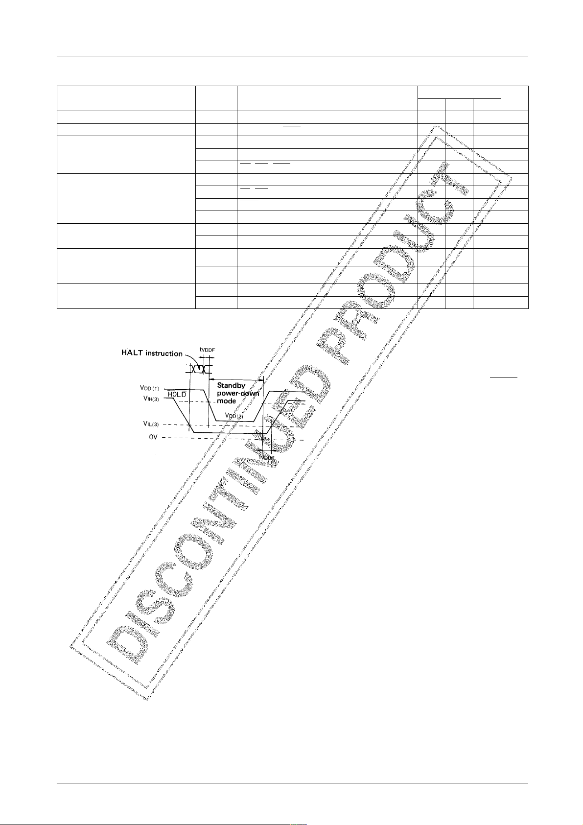
Fig. 1 Standby mode timing
[Note]
No chattering shall be applied to the HOLD
pin and PA0 to 3 pins during the HALT
instruction execution cycle.
No.2367–5/24
Page 6
LC6512A, LC6513A
Electrical Characteristics at Ta = –30 to +70°C, VDD = 5.0V±10%, VSS = 0V
retemaraPlobmySsnoitidnoC
tnerruclevel-hgihtupnII
tnerruclevel-woltupnII
egatlovlevel-hgihtuptuO
egatlovlevel-woltuptuO
tnerruckaelFFOtuptuO
CSOrotanoser
niardtnerruC
ecnaticapactupnIC
ecnaticapactuptuOC
egatlovsiseretsyHV
cimarecrofycneuqerfCSOkcolC
ecnaticapactuptuo/tupnIC
HI
LI
V
)1(HO
V
)2(HO
V
)3(HO
V
)4(HO
V
)5(HO
V
)6(HO
V
)7(HO
V
)8(HO
V
)1(LO
V
)2(LO
I
)1(FFO
I
)2(FFO
I
)3(FFO
I
)4(FFO
f
CSOFC
I
)1(DD
I
)2(DD
I
)3(DD
NI
TUO
OI
H
V:niptupnihcaE
NIV=DD
V:niptupnihcaE
NIV=SS
I:D,CstroP
I:D,CstroP
ItrophcaE(
I:H,GstroP
I:H,GstroP
I:2CSO
HO
I:D,CstroP
I:2CSO
LO
V:D,CstroP
V:D,CstroP
Am1–=V
HO
Aµ001–=V
HO
I:I,F,EstroP
I:I,F,EstroP
I:I,F,EstroP
HO
HO
HO
LO
V:edomTLAH
V:edomDLOH
Am01–=V
HO
Am2–=V
HO
Am1–=
HO
Am2–=V
Aµ001–=V
Am1= 4.0V
Aµ001= 4.0V
V=
TUO
DD
V=
TUO
SS
V:I,H,G,F,EstroP
V:I,H,G,F,EstroP
:2.giFnitiucricCSO2932etoN804zHk
DD
DD
DLOH,SER,TNI V1.0
)Am1–nahtsseL=
ItrophcaE(Am1–=
HO
edomDLOH,0.1Aµ
edomDLOH,0.1– Aµ
V=
TUO
DD
V=
TUO
.zHM3=fedomgnitarepO
V04– 03– Aµ
DD
zHk0001,008,004=f;CSOrotanosercimareC 0.10.2Am
Vniptupni,neponiptuptuo
V:derusaemgniebtonsniP
V:derusaemgniebtonsniP
V:derusaemgniebtonsniP
NIV=SS
.zHM1=ftaerusaeM:niptupnihcaE
SS
zHM1=ftaerusaeM:l,H,G,F,EstroP
SS
,zHM1=ftaerusaeM..D,CstroP
SS
3.giFnitiucrictseT,%01±V5=01Aµ
sgnitaR
nimpytxam
0.1Aµ
0.1– Aµ
0.2– V
DD
5.0– V
DD
8.1– V
DD
0.1– V
DD
V
5.0– V
DD
0.1– V
DD
)Am1–nahtsseL=V
CSOrotanosercimarecrofsnoitidnocdednemmoceR
,CSOrotanosercimarecrofsnoitidnocdednemmoceR
4.giFnitiucrictseT,V5.5ot8.1=01Aµ
5.0– V
DD
5.0– V
DD
4872etoN618zHk
0892etoN0201zHk
04922etoN0603zHk
7.20.4Am
5Fp
01Fp
01Fp
DD
03Aµ
tinU
V
No.2367–6/24
Page 7
LC6512A, LC6513A
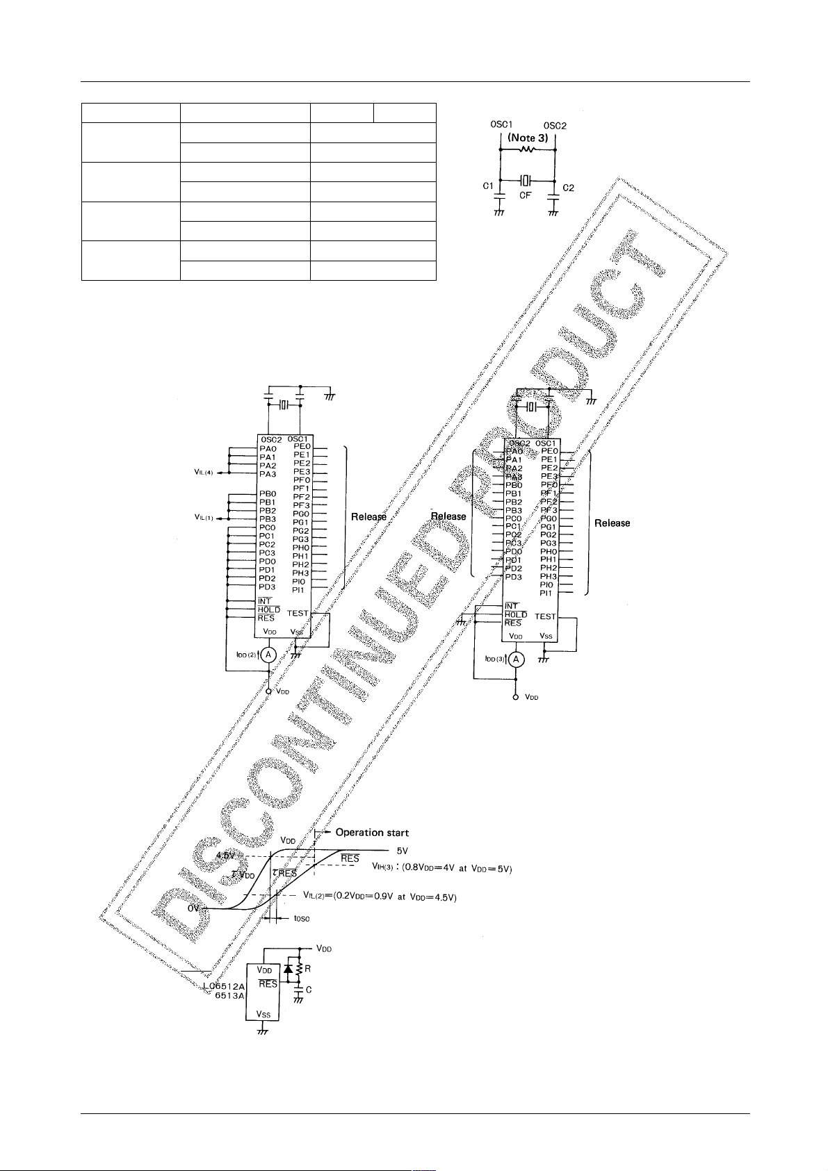
Center frequency
3MHz
1MHz
800kHz
400kHz
Ceramic resonator
CSA3.00MG (Murata)
KBR3.0MS (Kyocera) 22±10%
CSB1000K, D (Murata)
KBR1000H (Kyocera)
CSB800K, D (Murata)
KBR800H (Kyocera)
CSB400P (Murata)
KBR400B (Kyocera)
C1 (pF) C2 (pF)
33±10%
180±10%
180±10%
180±10%
180±10%
330±10%
330±10%
Fig. 2 Recommended OSC circuit, constants
for ceramic resonator OSC
CF: Ceramic resonator
CSA3.00MG (Murata)
KBR3.0MS (Kyocera)
CSB1000K, D (Murata)
KBR1000H (Kyocera)
CSB800K, D (Murata)
KBR800H (Kyocera)
CSB400P (Murata)
KBR400B (Kyocera)
Note 2) There is a tolerance of approximately 1% between the center frequency at the ceramic resonator mode and the
nominal value presented by the ceramic resonator supplier. For details, refer to the specification for the ceramic
resonator.
The min., max. values of OSC frequency represent the oscillatable frequency range.
Note 3) When using the piggyback microcomputer, evaluation chip for evaluation, connect a feedback resistor (approxi-
mately lMΩ).
Input/output common ports C, D: Output inhibit
HALT instruction is executed to provide HALT mode.
Fig. 3 IDD(2) test circuit Fig. 4 IDD(3) test circuit
Fig. 5 lnitial reset timing
τVDD: Power supply rise time constant
τ
: RES pin rise time constant
RES
Fix C. R so that τV
t
: OSC stabilized time
OSC
DD
<
τ
=
RES
, t
10ms. is obtained.
OSC
>
=
No.2367–7/24
Page 8

LC6512A, LC6513A
Appendix 1. Support System
For application development of the LC6512A, 6513A, the support system for the LC6512A, 6513A is used.
1-1. Software support
The support system provides source editor, cross assembler. For cross assembler on CP/M, the "LC6502.COM",
"LC6505.COM" are used, and on MS-DOS, the ''LC6512.COM", ''LC6513.COM" are used.
1-2. Hardware support
(1) Evaluation chip
Evaluation chip LC6597 is used. Level converters, drivers are connected to high-voltage ports (PE
to 3, PH0 to 3, PI0, 1) externally.
PG
0
to 3, PF0 to 3,
0
(A dedicated adaptor is available.)
External memory for program
Evaluation chip
General-purpose input
General-purpose input/output
FLT driver output
Fig. 1-1 Basic evaluation system using evaluation chip
(2) Simulation chip
Piggyback LC65PG12/13 and adaptor (EVA-97-12D/13D) for the LC6512A, 6513A are used jointly.
LC65PG12/13
EVA-97-12D/13D
A driver shown in fig. 1-3 is contained.
To user’s application aquipment
Fig. 1-2 How to use piggyback
Conversion board TB42S
No.2367–8/24
Page 9

LC6512A, LC6513A
(3) Evaluation kit
The EVA-410 and EVA-TB2 are used. For connecting with user's application equipment, adaptor (EVA-97-12D/
13D) is used.
(4) Adaptor (EV A-97-12D/13D)
This is used when evaluating the LC6512A, 6513A with the aid of the evaluation chip and piggyback. This
contains drivers for FLT. (See Figs. 1-3, 1-4.)
42-pin IC socket
•Evaluation kit
•Piggyback
-Vpp input
• Power supply for adaptor-contained
driver(LB1294)-Vpp for FLT is applied.
No external driver is required for
mass-produced microcomputers.
Fig. 1-3 Adaptor (EVA-97-12D/13D) for LC6512A, 6513A
Conversion board TB42S
User’s application board
(42-pin IC pin)
CN3
Conversion board
42-pin IC pin
CN2
Connector for
cable connection
NFP-50A-0112
(Yamaichi Electric-made)
CN1
Surface 42-pin socket
(Yamaichi Electric-made)
Fig. 1-4 EVA-97-12D/13D
IC1 to 3 (16pin)
LB1294 10pin : NC
IC4 (14pin)
LA6339
No.2367–9/24
Page 10

LC6512A, LC6513A
Appendix 2. lnternal Architecture of LC6512A, 6513A
The LC6512A, 6513A are identical with the LC6502C, 6505C in the internal architecture and instruction set except that
output ports are of high-voltage type and port A is of low-threshold input type and the standby function is the same as for
the LC6514B. For details, refer to ''LC6500 SERIES USER'S MANUAL''; and for the standb y function, refer to Appendix
4 ''Standby Function''.
2-1. PC
For the LC6512A, 6513A, this is organized with an 11-bit, 10-bit binary counter, respectively, which specifies the
ROM address of an instruction to be executed next. The high-order 3(2) bits specify a page and the low-order 8 bits
specify an address in the page. The page is updated automatically. ( ) is for the LC6513A.
2-2. ROM
This is used to store user programs. For the LC6512A, 6513A,this is organized with 2048x 8 bits, 1024 x 8 bits,
respectively. By using the ROM table read instruction, the whole area can be accessed and the display pattern can be
programmed.
2-3. Stack
This is used to save the contents of the PC at the subroutine call or interrupt mode. This allows subroutine nesting up
to 8 levels.
2-4. DP
This is a register organized with 4-bit DPL and 3-bit, 2-bit DPH for the LC6512A, 6513A, respectiv ely. When accessing the data RAM, the DPL, DPH specify a column address, row address, respectively. When accessing input/output
ports, the DPL specifies port A to port l. The DPL also specifies internal pseudo port O.
2-5. RAM
This is a static RAM used to store data. For the LC6512A, 6513A, this is organized with 128 x 4 bits, 64 x 4 bits,
respectively. Row addr ess 7H(3H) is allocated for 16 flags and 8 wor king registers which can be manipulated without
being addressed by the DP. ( ) is for the LC6513A.
2-6. AC, E
The AC is a 4-bit register which stores data to be processed by instructions. T he E register is an auxiliary register to be
back up the AC and is used as a temporary register or general-purpose register at the instruction execution mode.
2-7. ALU
This is a circuit which performs arithmetic and logic operations specified by individual instructions. This outputs not
only data of operation results but also the status of carry (C), zero (Z).
2-8. Status register
This is a 4-bit register which stores the status of carry, zero and the external interrupt, timer interrupt request.
The contents of the status register can be tested by the branch instructions.
2-9. Timer
This consists of a 4-bit fixed prescaler and an 8-bit programmable timer. This counts the system clock and requests a
timer interrupt when an overflow occurs.
2-10. Control register
This is a 4-bit register, 2-bits of which control input/output of input/output common ports C, D and 2-bits of which
enable/disable external interrupt, internal timer interrupt.
2-1 1. Input/output ports
There are 9 ports/34 pins from port A to I. Each port is ad dressed by the DPL. Ports A, B are of normal-volta ge input
type, ports C, D are of normal-voltage input/output common type, and ports E, F, G, H, I contain FLT drivers. Port A
is of low-threshold input type.
No.2367–10/24
Page 11

(1) Ports A0 to 3, B0 to 3
LC6512A, LC6513A
DSB---Input inhibit at HOLD mode
(2) Ports C
Functions • 4-bit input (IP instruction)
• Single-bit test (BP, BNP instructions)
• Port A: Low-threshold input
• Port B: Normal-threshold input
to 3, D0 to 3
0
Ports C,D
Output
inhibit
Ports A,B
Internal bus
DSB---Input output inhibit at HOLD mode
Output: High impedance
Internal bus
DSB---Output control (Control register)
(3) Ports E
Functions 1. Input mode (Output inhibit)
• 4-bit input (IP instruction)
• Single-bit test (BP, BNP instructions)
2. Output mode
• 4-bit output (OP instruction)
• Single-bit set, reset (SPB, RPB instructions)
to 3, F0 to 3, G0 to 3, H0 to 3, I0 to 1 (High-voltage ports)
0
DSB=Output inhibit at HOLD mode (Output transistor OFF)
Ports E to I
Functions • 4-bit (2-bit for port I) output (OP instruction)
• 4-bit (2-bit for port I) input of output latch contents (IP instruction)
• Single-bit set, reset (SPB, RPB instructions)
Set: The output represents a 1. ----- Output transistor ON
Reset: The output represents a 0. ----- Output transistor OFF
• Single-bit test of output latch contents (BP, BNP instructions)
• PortsE, F, I: FLT digits drive
• Ports G, H: FLT segments drive
Internal bus
No.2367–11/24
Page 12

LC6512A, LC6513A
2-12. External interrupt
The trailing edge of the signal on the INT pin is detected and the interrupt request flag in the status register is set. The
occurrence of an interrupt is controlled by the enable/disable flag in the control register.
2-13. Reset
The system is initialized by setting the RES pin to L-level. The contents to be initialized are as follows:
• PC Address 000H
• Control register 0000 → Interrupt disable, Ports C, D: Output inhibit
• Status register Timer, external interrupt flag → Reset
• Output port Output latch (0
Appendix 3. Proper Cares in Using IC
3-1. Low-threshold input port A
0
) → Output transistor OFF
H
to 3 provides the input characteristic shown in Fig. 3-1.
V
DD
High-level input
1.9V
0.5V
V
SS
Low-level input
Fig. 3-1
3-2. FLT driver output
Ports E
to 3, F0 to 3, I0 to 1 (10 pins) are for high-current digits driver output; and ports G0 to 3, H0 to 3 (8 pins) are for
0
intermediate-current segments driver outputs. Of course, digits driver outputs can be used as segments driver outputs.
Fig. 3-2 shows a sample application.
Key scan
Ports E,F,I
Ports G, H
LC6512A, 6513A
-Vpp
-Vpp
Segments
Digits
Fig. 3-2 FLT display application
No.2367–12/24
Page 13
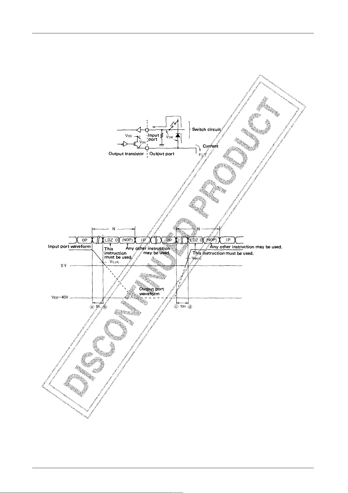
LC6512A, LC6513A
Digit drive signal-used key scan
When key-scanning with the FLT digit driv e signal in Fig. 3-3 and inputting the return signal to port A, the following must
be observed.
(a) Estimate voltage drop (V
characteristic of the output port of the LC6512A, 6513A.
(b) Estimate voltage drop (VSW)in the switch circuit.
(c) Check to see that V
ON
For the key scan application in Fig. 3-3, make the program considering the delay in the external circuit and the input delay
shown below.
) in the output transistor using the current flowing in an FLT used and the V-I
ON
+ VSW meets the VIH/VIL requirement of the input port in Fig. 3-1.
tDL tDH (External circuit delay time)
Fig. 3-3 Sample key scan application
Fig. 3-4
When the IP instruction is used to input the return signal as shown above, the input delay must be considered and two
, V
instructions are placed between the IP instruction and the crossing of input port waveform and V
IL(4)
, respectively.
IH(1)
Some instructions must be placed additionally according to the length of delay (tDL, tDH) in the external circuit after the
digit drive signal is delivered with the execution of the OP instruction (point a and point c).
N: Number of instruction cycles existing between instruction (OP, SPB, RPB) used to output data to output port and
instruction (IP, BP, BNP) used to input data from input port.
(Number of instruction cycles to be programmed according to the length of t
DL
, tDH)
tDL, tDH: Delay in external circuit from output port to input port.
No.2367–13/24
Page 14

LC6512A, LC6513A
Appendix 4. Standby Function
Two standby modes – HALT mode and HOLD mode – are available to minimize the power dissipation when the program
is in the wait state or a power failure is backed up. Both modes are set with the e xecution of the HALT instruction. All the
operations including the system clock generator are stopped at the standby mode. (For other models LC6502/05 of the
LC6500 series, the HOLD mode is hardware-set with the HOLD pin = "L". Be careful of the difference in the mode setting
method.)
The HALT mode and HOLD mode are used properly depending on the purposes. They are different in the mode setting
conditions, I/O port state during standby operation, mode releasing method. The HALT mode is entered by executing the
HALT instruction when the HOLD pin is at H-Level. The HALT mode is used to save the power dissipation when the
program is in the wait state. The HOLD mode is entered by executing the HALT instruction when the HOLD pin is at LLevel. At the HOLD mode all I/O ports are disabled and there is no power dissipation in the interfaces with external
circuits, permitting capacitor or battery-used power supply backup during power failure.
4-1. HALT mode setting
The HALT mode is entered by executing the HALT instruction when the HOLD pin is at H-Level and all pins for port
to A3 are at L-Level. When even one of pins for port A0 to A3 is at H-Level, the HALT instruction is disregarded
A
0
and becomes equal to the NOP instruction.
The HALT mode causes individual blocks to be placed in the following states.
Operation is stopped
(1)
• All the operations including the system clock generator are stopped.
I/O port
(2)
• The state immediately before setting the HALT mode is held.
Blocks to be cleared/reset
(3)
• Timer............State where all bits are set to "1"(max.time).
• Status flag.....The EXTF, TMF are reset (interrupt disable). The CF, ZF contents are held. An interrupt request at the
HALT mode is disregarded.
Blocks to be held
(4)
• For the registers, data RAM, port output latch, PC (except those in (3), the contents immediately before setting the
HALT mode are held.
4-2. HOLD mode setting
The HOLD mode is entered by executing the HALT instruction when the HOLD pin is at L-Level. ln this case, the
contents of port A
to A3 remain unaffected.
0
The state in the HOLD mode is the same as that in the HALT mode, except the state of I/O port. The HOLD mode
permits the undermentioned power-down mode to be entered.
I/O port
• lnput ports A, B: lnput inhibit
• Input/output port C, D: Input inhibit, output high impedance
• Output ports E to I: Output Pch transistor OFF
• INT, RES pins: Input inhibit
For the output latch of the output port, the contents immediately before setting the HOLD mode are held.
No.2367–14/24
Page 15

LC6512A, LC6513A
4-3. HOLD power-down mode setting
The HOLD mode permits the supply voltage to be lowered and also the power dissipation to be reduced after mode
setting. The HOLD mode can be used in the capacitor or battery-used backup operation during power failure.
Fig. 4-1 HOLD mode and power-down
¡ A failure of the main power supply is detected and a standby request is made. This is hardware-controlled by the
external circuit.
™ The HOLD pin is software-polled or the same signal is applied to the INT pin to test the standby request by
interrupt. Then, the HALT instruction is executed and the HOLD mode is entered. (Note)
£ After the HOLD mode is entered, power-down can be attained by lowering V
¢ After V
returns to the prescribed voltage, the HOLD pin is set to H-Level and the normal operation returns.
DD
DD
.
0
(Note) The HOLD pin input signal is transferred to pseudo input port PO 0 (DPL = 0EH, 2
bit). Therefore, when
polling the HOLD pin, the BP0 or BNP0 instruction is used at DPL = 0EH. (The IP instruction cannot be
used.)
When the BP0 instruction is used for testing, a branch occurs when the input voltage is at high level in the
same manner as for normal input ports.
4-4. HALT mode release
Release by reset
When L-Level is applied to the RES pin, the HALT mode is released and the system reset state is entered.
When the RES pin is set to H-Level again, the normal operation starts. Since the ceremic resonator mode is used for
system clock generation, the release by reset must be performed.
–Notes–
• Since the ceramic resonator mode is used for system clock generation, L-Level must be applied to the RES pin for 5
to 10 ms (oscillation stabilizing time).
Mode change from HALT mode to HOLD Mode
The HALT mode is entered with the execution of the HALT instruction when the HOLD pin is at H-Level.
The HALT mode is changed to the HOLD mode automatically by setting the HOLD pin to L-Level.
Fig. 4-2 Mode change from HALT modeto HOLD mode
No.2367–15/24
Page 16
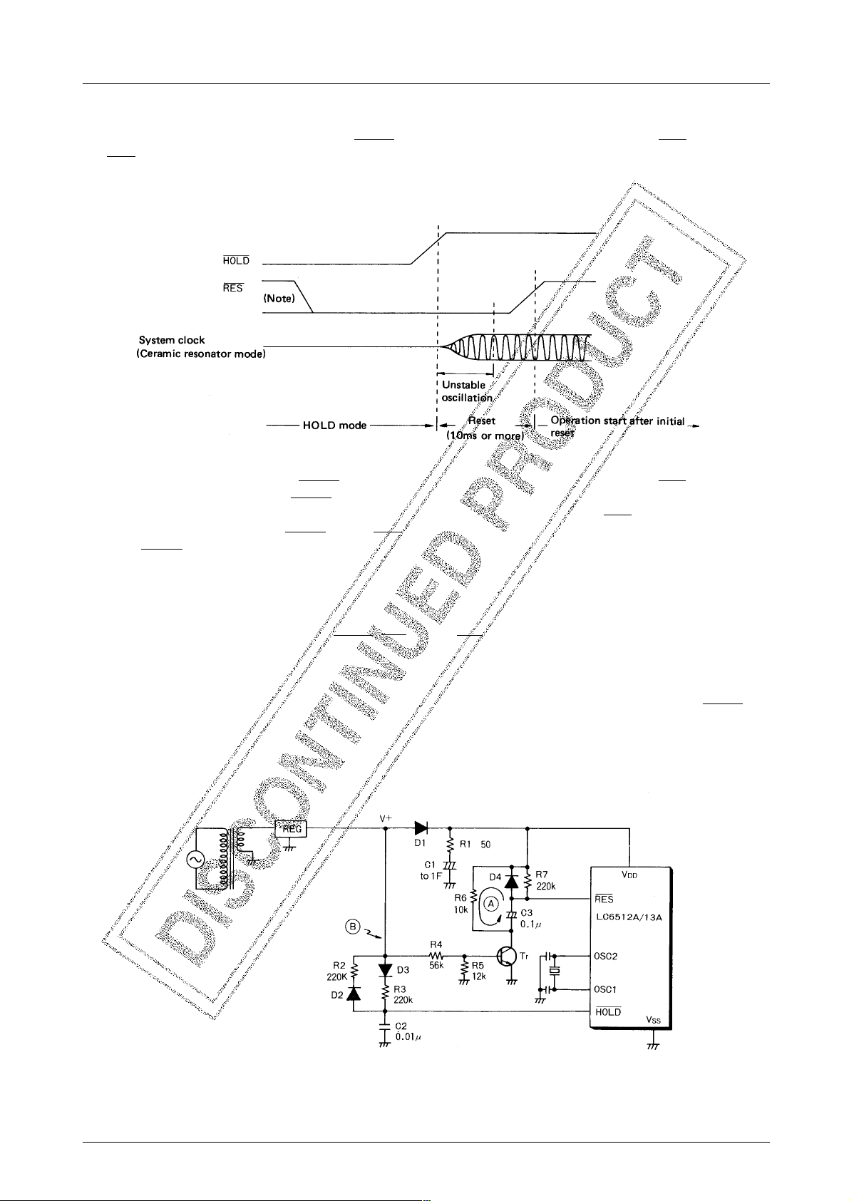
LC6512A, LC6513A
4-5. HOLD mode release
Release by reset
The HOLD mode is released by setting the HOLD pin to H-Level while applying L-Level to the RES pin. When the
RES pin is set to H-Level again, the normal operation starts. The contents of the memories remain unaffected except
the PC, I/O ports, registers which are initialized by the reset operation.
Since the ceramic resonator mode is used, the reset state must be held until oscillation is fully stabilized (10 ms after
oscillation start) after the HOLD mode is released.
Fig. 4-3 HOLD mode release by reset
Note: W ith L-Level applied to the HOLD pin as shown abov e , the CPU is not reset e ven when the RES pin is set to L-
Level. This is because the HOLD pin is given priority lest the CPU is reset unnecessarily when the capacitor or
battery-used backup mode causes the CPU peripherals to operate unstably and the RES pin is set to L-Level. Be
careful of the level of the HOLD pin and RES pin also at the initial reset mode when power is a pplied. When the
HOLD pin is at L-Level, no reset occurs.
4-6. Proper cares in using standby function
When using the HOLD mode, an application circuit and program must be designed with the following in mind.
(1) The supply voltage at the standby state must not be less than specified.
(2) Input timing of each control signal (HOLD, RES, port A, INT, etc.) at the standby initiate/release state.
(3) Release operation must not be overlapped at the time of execution of the HALT instruction.
4-7. Sample application where the standby function is used for power failure backup
Power failure backup is an application where power failure of the main power source is detected by the HOLD pin,
etc. to cause the HOLD mode to be entered so that the current drain is minimized and a backup capacitor is used to
retain the contents of the internal registers even during power failure.
4-7-1. Sample application circuit (ceramic resonator OSC)
Fig. 4-4 shows a ceramic resonator OSC-applied circuit where the standby function is used for power failure backup.
100V
AC
Power
Supply
Unit(resistance:Ω, capacitance:F)
Fig. 4-4 Sample Application Circuit
No.2367–16/24
Page 17

LC6512A, LC6513A
4-7-2. Operating waveform
The operating waveform in the sample application circuit in Fig. 4-4 is shown below. The mode is roughly divided as
follows:
⁄ Initial application of power ¤ Instantaneous break-(2) ¤ Instantaneous break-(3)
‹ Return from backup voltage
4-7-3. Operation of sample application circuit
¡ At the time of initial application of power
A reset occurs and the execution of the program starts at address 000H of the program counter (PC).
™ At the time of instantaneous break
(1) At the time of very short instantaneous break
The execution of the program continues.
(2) At the time of instantaneous break being a little longer than (1) (When the RES input v olta ge meets V
HOLD input voltage does not meet V
).
IL
A reset occurs during the execution of the program and the execution of the program starts at address 000H of
the program counter (PC).
Since the HOLD request signal is not applied to the HOLD pin, the HOLD mode is not entered.
(3) At the time of long instantaneous break (When both of the RES input voltage and HOLD input voltage meet
).
V
IL
The HOLD request signal is applied to the HOLD pin and the HOLD mode is entered.
When V+ rises after instantaneous break, a reset occurs to release the HOLD mode and the execution of the
program starts at address 000H of the program counter (PC).
£ At the time of return from backup voltage
A reset occurs and the execution of the program starts at address 000H of the program counter (PC).
and the
IL
No.2367–17/24
Page 18

LC6512A, LC6513A
4-7-4. Notes for circuit design
¡ How to fix C3, R6, C2, R2
Fix closed loop (A) discharge time constants C3, R6 and HOLD pin charge time constants C2, R2 so that closed
loop (A) fully discharges before the HOLD input voltage gets lo wer than V
the RES input voltage is sure to get lower than V
the HOLD input voltage gets lower than V
IL
(a reset occurs) when V+ rises after instantaneous break where
IL
.
™ How to fix C3, R7
Fix RES pin charge time constants C3, R7 so that when power is applied initially or the HOLD mode is released the
ceramic resonator OSC oscillates normally and the RES input voltage exceeds V
£ How to fix R4, R5
Fix Tr bias constants R4, R5 so that when V+ rises after instantaneous break the RES input voltage gets lo wer than
(brought to L-Level) before the HOLD input voltage exceeds VIH (brought to H- Level).
V
IL
¢ How to fix C2, R3
Fix HOLD pin charge time constants C2, R3 so that when the HOLD mode is released from the backup mode the
HOLD input voltage does not exceed V
(not brought to H-Level) until the RES input voltage gets lo wer than V
OH
(brought to L-Level).
Fix C3, R7 and C2, R3 so that the time interval from the moment the HOLD input voltage exceeds V
moment the RES input voltage exceeds V
is longer than the ceremic resonator OSC stabilizing time.
IH
∞ When the load is heavy or the polling interval is long
Since Cl discharges largely, increase the capacity of C1 or separate (B) detection from V+ and use a power supply
or signal that rises faster than V+.
at the time of instantaneous break and
IL
and the program starts running.
IH
until the
IH
IL
4-7-5. Notes for software design
When the HOLD request signal is detected, the HALT instruction is executed immediately. A concrete example is
shown below.
(1) An interrupt is inhibited before polling the HOLD request pin (HOLD pin).
(2) Polling of the HOLD pin and the HALT instruction are programmed consecutively.
[ Concrete example ]
……
RCTL 3 ;EXTEN, TMEN ← 0 (External, timer interrupt inhibit)
BP0 AAA ;Polling of the HOLD pin (If H-Level, a branch occurs to AAA.)
HALT ;The HOLD mode is entered.
AAA:
No.2367–18/24
Page 19

LC6512A, LC6513A
Appendix LC6500 Series Instruction Set (by Function)
Symbols Meaning
AC : Accumulator
ACt: Accumulator bit t
CF: Carry flag
CTL: Control register
DP: Data pointer
E : E register
EXTF: External interrupt request flag
Fn: Flag bit n
Mnemonic
Instruction
CLA
CLC
STC
CMA
INC
DEC
RAL
TAE
Accumulator manipulation instructions
XAE
INM
DEM
SMB bit
RMB bit
Memory manipulation
instructions
AD
ADC
DAA
DAS
EXL
AND
OR
CM
Operation/comparison instructions
CI data
CLI data
LI data
S
L
XM data
X
XI
Load/store instructions
XD
RTBL
Clear AC 0 0 0 0 AC ← 0111 1 0 0
Set CF
Complement AC
Increment AC
Decrement AC
Rotate AC left through
CF
Tranfer AC to E
Exchange AC with E
lncrement M
Decrement M
Set M data bit
Reset M data bit
Add M to AC
Add M to AC with CF
Decimal adjust AC in
addition
Decimal adjust AC in
Subtraction
Exclusive or M to AC
And M to AC
Or M to AC
Compare AC with M
Compare AC with
immediate data
Compare DPL with
immediate data
Load AC with
immediate data
Store AC to M
Load AC from M
Exchange AC with
M.then modify DPH
with immediate data
Exchange AC with M
then increment DPL
Exchange AC wIth M.
then decrement DPL
program ROM
Instruction code
D7D6D5D
1 1 1 0
0 0 0 0
0 0 0 0
0 0 0 0
0 0 0 0
0 0 0 0
0 0 1 0
0 0 1 0
0 0 0 0
0 0 1 0
0 1 1 0
0 0 1 0
1 1 1 0
1 1 1 0
1 1 1 1
1 1 1 0
1 1 1 0
1 1 1 1
0 0 1 0
0 1 0 0
0 0 1 0
0 1 0 1
1 1 0 0
0 0 0 0
0 0 1 0
1 0 1 0
1 0 1 0 1
1 1 1 1
0 1 1 0 0 0 1 1Read table data from
M: Memory
M(DP): Memory addressed by DP
P(DPL): Input/output port addressed by DPL
PC: Program counter
STACK: Stack register
TM : Timer
TMF : Timer (internal) interrupt request flag
At, Ha, La: Working register
ZF: Zero flag
D3D2D1D
4
0 0 0 1
0 0 0 1 11 1 1 1 1
1 1 1 0
1 1 1 1
0 0 0 1
0 0 1 1
1 1 0 1
1 1 1 0
1 1 1 1
10B1B
0
10B1B
0
0 0 0 0
0 0 0 0
0 1 1 0
1 0 1 0
0 1 0 1
0 1 1 1
0 1 0 1
1 0 1 1
1 1 0 0
I3I2I1I
0
1 1 0 0
I3I2I1I
0
I3I2I1I
0
0 0 1 0
0 0 0 1
0M2M1M
0
1 1 1 1
Bytes
0
1
11 0 1 1
1
1
1
1
1
1
1
1
1
1
1
1
1
1
1
1
1
2
2
1
1
1
1
11 1 1 1 1 1 1 0Exchange AC with M.
Function
Cycles
11 1 1 0 Clear CF CF ← 0
CF ← 1
AC ← (AC)
1
AC ← (AC)+1
1
AC ← (AC)–1
1
AC0←(CF).AC
1
(ACn). CF←(AC3)
1
E←(AC)
→
1
(AC)←(E)
1
M(DP)←[M(DP)]+1
1
M(DP)←[M(DP)]–1
1
M(DP. B1B0)–1
1
M(DP. B1B0)←0
1
AC ←(AC)+[M(DP)]
AC←(AC)+[M(DP)]
1
+(CF)
1
AC←(AC)+6
1
AC←(AC)+10
1
AC←(AC) [M(DP)]
AC←(AC)
1
1
AC←(AC) [M(DP)]
1
[M(DP)]+(AC)+1
2
I3 I2 I1 l0+(AC)+1
2
(DP
1
AC←I3 I2 I1 l
1
M(DP) ←(AC)
AC←[M(DP)]
1
(AC) [M(DP)]
2
DPH ←(DPH)
• 0M2M1M
(AC) [M(DP)]
20 0 0 0
2 (AC) [M(DP)]
DP
21 (AC) [M(DP)]
DP
AC. E←ROM
21
L
) I3 I2 I1 l
←
←
←
←
←
←
L
←(DPL)+1
←
←
L
←(DPL)–1
(PCh.E. AC)
←
n+1
[M(DP)]
0
0
0
( ),[ ]: Contents
← : Transfer and direction
+ : Addition
– : Subtraction
<
: AND
: OR
<
<
: Exclusive OR
Description
The AC contents are cleared.
The CF is reset.
The CF is set.
The AC contents are complemented
(zero bits become 1,one bits become 0)
The AC contents are incremented +1.
The AC contents are decremented –1.
The AC contents are shifted left through the
CF.
The AC contents are transferred to the E.
The AC contents and the E contents are
exchanged.
The M(DP) contents are incrementcd +1.
The M (DP) contents are decremented –1.
A single bit of the M(DP)specified by B1 B0
is set.
A single bit of the M(DP) specified by B1 B0
is reset.
The AC contents and the M(DP) contents
are binary-added and the result is placed in
the AC.
The AC,CF, M(DP) contents are binaryadded and the result is placed in the AC.
6 is added and to the AC contens.
10 is added to the AC contents.
The AC contents and the M(DP) contents
are exelusive-ORed and the result is placed
in the AC.
The AC contents and the M(DP) contents
are ANDed and the result is placed in the
AC.
The AC contents and the M(DP) contents
are ORed and the result is placed in the AC.
The AC contents and the M(DP) contents
are compared and the CF and ZF are
set/reset.
ZFComparison result
CF
[M(DP)] >(AC)
[M(DP)] =(AC)
[M(DP)] <(AC)
The AC contents and immediate data
I3 I2 I1 I
are compared and the ZF and CF
0
are set/reset.
I3I2l1l0 >(AC)
I3I2l1l0 =(AC)
I3I2l1l0 <(AC)
The DPL contents and immediate data
I3 I2 I1 I0 are compared.
Immediate data I3 I2 I1 I0 in loaded in the
AC.
The AC contents are stored in the M(DP).
The M(DP) contents are loaded in the AC.
The AC contents and the M(DP) contents
are exchanged.Then, the DPH contents are
modified with the contens of(DPH)
0M2M1M0.
The AC contents and the M(DP) contents
are exchanged.
The AC contents and the M(DP) contents
are exchanged.Then, the DPL contents are
incremented +1.
The AC contents and the M(DP) contents
are exchanged.Then, the DPL contents are
decremented –1.
The contents of ROM addressed by the PC
whose low-order 8 bits are replaced with the E
and AC contents are loaded in the AC and E.
0
0
1
1
0
1
ZFComparison result
CF
0
0
1
1
0
1
Status
flag
affected
ZF
CF
CF
ZF
ZF CF
ZF CF
ZF CF
ZF CF
ZF CF
ZF
ZF CF
ZF CF
ZF
ZF
ZF
ZF
ZF
ZF CF
ZF CF
ZF
ZF
ZF
ZF
ZF
ZF
ZF
Remarks
∗1
∗1
The ZF is set/
reset accoding to
the result of (DPH)
0M2M1M0.
The ZF is set/reset
accoding to the
DPH contents at
the time of instruction execution.
The ZF is set/reset
accoding to the
result of (DPL +1).
The ZF is set/reset
accoding to the
result of (DPL–1).
No.2367–19/24
Page 20

LC6512A, LC6513A
Mnemonic
Instruction
Load DPH With Zero and
date
LHI data
DPL with immediate data
respectively
Load DPH with
immediate data
lND
DED
TAL
TLA
XAH
Data pointer manipulation instructions
XAt
instructions
XHa
XLa
Working register manipulation
SFB flag
RFB
XA0
XA1
XA2
XA3
XH0
XH1
XL0
XL1
Increment DP
Decrement DP
L
L
Transfer AC to DP
Transfer DPL to AC
Exchange AC with
DPH
Exchange AC with
working register At
Exchange DPH with
working register Ha
Exchange DPL with
working register La
Set flag bit
Reset flag bit
flag
Flag manipulation instructionsBranch instructions
JMP
addr
JPEA
CZP
addr
CAL
addr
Jump/subroutine instructions
RT
RTI
Jump in the current
bank
Jump in the current
page modified by E
and AC
Call subroutine in the
Zero Page
Call subroutine in the
zero bank
Return from
subroutine
Returnn from interrupt
routine
BAt
Branch on AC bit
addr
BNAt
Branch on no AC bit
addr
BMt
Branch on M bit
addr
BNMt
Branch on no M bit
addr
BPt
Branch on Port bit
addr
BNPt
addr
BTTM
Branch on timer
addr
D7D6D5D
L
P7P6P5P4
P7P6P5P4
P7P6P5P4
P7P6P5P4
P7P6P5P4
P7P6P5P4
P7P6P5P4
P7P6P5P4
P7P6P5P4
Instruction code
D3D2D1D
4
1 0 0 0 LDZ
I3 I2 I1 I01
0 1 0 0
1 1 1 0
1 1 1 0
1 1 1 0
1 1 1 1
0 1 1 1
1 1 1 0
0 0 1 0
1 1 1 0
1 1 1 0
1 1 1 0
1 1 1 0
1 1 1 1
1 1 1 1
1 1 1 1
1 1 1 1
0 1 0 1
0 0 0 1
0 1 1 0
1 1 1 1
1 0 1 1
1 0 1 0
0 1 1 0
0 0 1 0
0 1 1 1
0 0 1 1
0 1 1 1
0 0 1 1
0 1 1 1
0 0 1 1
1 0 0 1
0 0 1 1
t1 t0
0 0 0 0
0 1 0 0
1 0 0 0
1 1 0 0
a
1 0 0 0
1 1 0 0
a
0 0 0 0
0 1 0 0
B3B2B1B
B3B2B1B
1 P10P9P
P3P2P1P
1 0 1 0
P3P2P1P
1 P10P9P
P3P2P1P
0 0 1 0
0 0 1 0
0 0 t1 t
P3P2P1P
0 0 t1 t
P3P2P1P
0 1 t1 t
P3P2P1P
0 1 t1 t
P3P2P1P
1 0 t1 t
P3P2P1P
1 0 t1 t
P3P2P1P
1 1 0 0
P3P2P1P
0
0
0
0
8
0
0
8
0
0
0
0
0
0
0
0
0
0
0
0
0
0
Bytes
Cycles
1
DPH←0
DPL←I3I2I1I
11I3 I2 I1 I
DPH←I3I2I1I
DPL←(DPL)+111
DPL←(DPL)–1
1
1
1
11 1 1 1
DPL←(AC)
1
1
AC←(DPL)
1
1
(AC) (DPH)
1
1
(AC) (A0)
1
1
(AC) (A1)
1
1
(AC) (A2)
1
1
(AC) (A3)
1
1
(DPH) (H0)
1
1
(DPH) (H1)
1
1
(DPL) (L0)
1
1
(DPL) (L1)
1
1
Fn←1
1
1
Fn←0
PC←PC11(orPC11)
2
2
P10P9P8P7P6P
P4P3P2P1P
1
PC
1
STACK←(PC)+1
1
1
PC
PC
STACK←(PC)+2
2
2
PC
P8P7P6P5P4P3P2P1P
PC←(STACK)
1
1
PC←(STACK)
1
1
CF ZF←CSF.ZSF
PC
2
2
P3P2P1P
If ACt=1
PC
2
2
P3P2P1P
If ACt=0
PC
2
2
P3P2P1P
If [M(DP.t1t0)]=1
2
2
PC
P3P2P1P
If [M(DP.t1t0)]=0
2
PC
P3P2P1P
If [P(DPL.t1t0)]=1
PC
222Branch on no Port bit
P3P2P1P
If [P(DPL.t1t0)]=0
PC7 to 0←P7P6P5P4
22
P3P2P1P0
If TMF=1
then TMF←0
Function
0
0
←
←
←
←
←
←
←
←
←
←
←
←
←
←
←
←
←
←
5
0
←(E, AC)
7 to 0
←OP10P
←0
9
11 to 6.PC1 to 0
5 to 2←P3P2P1P0
11* to 0
7 to 0←P7P6P5P4
7 to 0←P7P6P5P4
7 to 0←P7P6P5P4
7 to 0←P7P6P5P4
7 to 0←P7P6P5P4
7 to 0←P7P6P5P4
Description
The DPH and DPL are loaded with 0 and
immediate data I3I2I1I0 respectively.
The DPH is loaded with immediate
data I3I2I1I0.
The DPL contents are incremented
+1.
The DPL contents are decremented
–1.
The AC contents are transferred to
the DPL.
The DPL contents are transferred to
the AC.
The AC contents and the DPH
contents are exchanged.
The AC contents and the contents of
working register A0, A1, A2, or A3
specified by t1 t0 are exchanged.
The DPH contents and the contents
of working register H0 or H1 specified
by a are exchanged.
The DPL contents and the contents of
working register L0 or L1 specified by
a are exchanged.
A flag specified by B3B2B1B0 is set.
A flag specified by B3B2B1B0 is
reset.
A jump to an address specified by the
PC11(or PC11)and immediate data
P10 to P0 occurs.
A jump to an address specified by the
contents of the PC whose low-order 8
bits are replaced with the E and AC
contents occurs.
A subroutine in page 0 of bank 0 is
called.
A subroutine in bank 0 is called.
0
A return from a subroutine occurs.
A return from an lnterrupt servicing
routine occurs.
If a single bit of the AC specified by
immediate data t1 t0 is 1,a branch to an
0
address specified by immediate data P7
to P0 within the current page occurs.
If a single bit of the AC specified by
immediate data t1t0 is 0,a branch to an
0
address specified by immediate data P7
to P0 within the current page occurs.
If a single bit of the M(DP) specified by
immediate data t1t0 is 1,a branch to an
0
address specified by immediate data P7
to P0 within the current page occurs.
If a single bit of the M(DP) specified by
immediate data t1t0 is 0,a branch to an
0
address specified by immediate data P7
to P0 within the current page occurs.
If a single bit of port P(DPL) specified by
immediate data t1 t0 is 1,a branch to an
0
address specified by immediate data P7
toP0 within the current page occurs.
If a single bit of port P(DPL) specified by
immediate data t1 t0 is 0,a branch to an
0
address specified by immediate data P7
to P0 within the current page occurs.
If theTMF is 1,a branch to an address
specified by immediate data P7 to P0
within the current page occurs.The TMF
is reset.
Status
flag
affected
ZF
ZF
ZF
ZF
ZF CF
TMF0 1 1 1
Remarks
The flags are
divided into 4
groups of F0 to
F3,F4 to F7,F8 to
F11,F12 to F15.
The ZF is set/reset
according to the 4
bits including a
single bit specified
bit specified by
immediate data
B3B2B1B0.
Mnemonic is
BA0 to BA3
according to
the value of t.
Mnemonic is
BNA0 to BNA3
according to
the value of t.
Mnemonic is
BM0 to BM3
according to
the value of t.
Mnemonic is
BNM0 to
BNM3
according to
the value of t.
Mnemonic is
BP0 to BP3
according to
the value of t.
Mnemonic is
BNP0 to BNP3
according to
the value of t.
No.2367–20/24
Page 21

LC6512A, LC6513A
Mnemonic
Instruction
BNTM
Branch on no timer
addr
BI addr
BNI
Branch on interrupt 1 1 0 1
Branch on no lnterrupt
addr
BC addr
BNC
Branch on CF
Branch on no CF
addr
BZ addr
Branch instructions
BNZ
Branch on ZF
Branch on no ZF
addr
BFn
Branch on flag bit
addr
BNFn
Branch on no flag bit
addr
IP
OP
SPB bit
RPB bit
Input port to AC
Output AC to port
Set port bit
Reset port bit
Input/Output instructions.Other instructions
SCTL
bit
RCTL
bit
WTTM
Set control register
bit(S)
Reset control register
bit(S)
Write timer
HALT 1 1 1 1Halt
NOP
No operation 110 0 0 00 0 0 0 No operation
Instruction code
D7D6D5D
D3D2D1D
4
0 0 1 1
P7P6P5P4
P3P2P1P0
0 1 1 1
P7P6P5P
P3P2P1P0
4
0 0 1 1
P7P6P5P
P3P2P1P0
4
0 1 1 1
P7P6P5P
4
0 0 1 l
P7P6P5P
4
0 1 1 l
P7P6P5P
4
0 0 l l
P7P6P5P
4
1 1 0 1
P7P6P5P
4
1 0 0 1
P7P6P5P
4
0 0 0 0
0 1 1 0
0 0 0 0
0 0 1 0
0 0 1 0
1 0 0 0
B
0 0 1 0
1 0 0 1
B
1 1 1 1
1 1 0 1
P3P2P1P
1 1 1 1
P3P2P1P
1 1 1 0
P3P2P1P
1 1 1 0
P3P2P1P
n3n2n1n
P3P2P1P
n3n2n1n
P3P2P1P
1 1 0 0
0 0 0 1
0 1 B1B
0 1 B1B
1 1 0 0
3B2B1B0
1 1 0 0
3B2B1B0
0 1 1 0
Bytes
0
21 1 0 0
2
21 1 1 1
0
222
0
2
0
2
0
0
0
2
0
0
1
1
1
0
1
0
2
2
11 0 0 1
Function
Cycles
PC
2
7 to 0←P7P6P5P4
P3P2P1P
If TMF=0
then TMF←0
PC
2
7 to 0←P7P6P5P4
P3P2P1P
If EXTF=1
then EXTF←0
PC
22
7 to 0←P7P6P5P4
P3P2P1P
If EXTF=0
then EXTF←0
PC
2
7 to 0←P7P6P5P4
P3P2P1P
If CF=1
PC
7 to 0←P7P6P5P4
P3P2P1P
If CF=0
PC
2
7 to 0←P7P6P5P4
P3P2P1P
If ZF=1
PC
2
7 to 0←P7P6P5P4
P3P2P1P
If ZF=0
PC
2
7 to 0←P7P6P5P4
P3P2P1P
If Fn=1
PC
2
7 to 0←P7P6P5P4
P3P2P1P
If Fn=0
AC←[P(DPL)]
1
1
P(DPL)←(AC)
P(DPL B1B0)←1
2
P(DPL B1B0)←0
2
CTL←(CTL)
2
B3B2B1B
CTL←(CTL)
2
B3B2B1B
1TM←(E).(AC)
TMF ←0
Halt All operations stop.11
Description
If the TMF is 0, a branch to an
address specified by immediate data
0
P7 to P0 within the current page
occurs. The TMF is reset.
If the EXTF is 1, a branch to an
address specified by immediate data
0
P7 to P0 within the current page
occurs. The EXTF is reset.
If the EXTF is 0, a brance to an
address specified by immediate data
0
P7 to P0 within the current page
occurs. The EXTF is reset.
If the CF is 1, a branch to an address
specified by immediate data P7 to P0
0
within the current page occurs.
If the CF is 0, a branch to an address
specified by immediate data P7 to P0
0
within the current page occurs.
If the ZF is 1, a branch to an address
specified by immediate data P7 to P0
0
within the current page occurs.
If the ZF is 0, a branch to an address
specified by immediate data P7 to P0
0
within the current page occurs.
If a fiag bit of the 16 flags specified by
immediate data n3n2n1n0 is 1,a branch to
0
an address specified by immediate data P7
to P0 within the current page occurs.
If a fiag bit of the 16 flags specified by
immediate data n3n2n1n0 is 1,a branch to
0
an address specified by immediate data P7
to P0 within the current page occurs.
The contents of port P(DPL) are inputted to
the AC.
The AC contents are outputted to port
P(DPL)
Immediate data B1B0- specified one
bit in port p(DPL)is set.
Immediate data B1B0- specified one
bit in port p(DPL)is reset.
Immediate data B3B2B1B0-specified
bits in the control register are set.
0
Immediate data B3B2B1B0-specified
bits in the control register are reset.
0
The E and AC contents are loaded in
the timer. The TMF reset.
Status
flag
affected
TMF
EXTF
EXTF
ZF
ZF
ZF
TMF
No operation is performed, but 1
machine cycle is consumed.
*1 lf the LI instruction or CLA instruction is used consecutively in such a manner as LI, LI, LI……,or CLA,
CLA, CLA, ……, the first LI instruction or CLA instruction only is effective and the following LI instructions or CLA instructions are changed to the NOP instructions.
Remarks
Mnemonic is
BFO to BF15
according to
the value of n.
Mnemonic is
BNFO to
BNF15
according to
the value of n.
Mnemonic is
BNFO to BNF15
according to the
value of n.
When this instruction is executed,the
E register contents
are destroyed.
No.2367–21/24
Page 22

LC6500 Series Instruction Map
LC6512A, LC6513A
No.2367–22/24
Page 23

LC6500 Series Programming Model
LC6512A, LC6513A
-----Suffix Z, C represent that the ZF, CF flags of the status register are affected.
conditions are met immediate data of ROM is loaded in the PC.
BAt BPt BI BZ
(1) The Branch instructions include the following instructions, and only when the branch
Note
No.2367–23/24
Z,C
BNAt BNPt BNI BNZ
BMt BTM BC BFn
BNMt BNTM BNC BNFn
(2)AC
Page 24

LC6512A, LC6513A
Specifications of any and all SANYO products described or contained herein stipulate the performance,
characteristics, and functions of the described products in the independent state, and are not guarantees
of the performance, characteristics, and functions of the described products as mounted in the customer's
products or equipment. To verify symptoms and states that cannot be evaluated in an independent device,
the customer should always evaluate and test devices mounted in the customer's products or equipment.
SANYO Electric Co., Ltd. strives to supply high-quality high-reliability products. However, any and all
semiconductor products fail with some probability. It is possible that these probabilistic failures could
give rise to accidents or events that could endanger human lives, that could give rise to smoke or fire,
or that could cause damage to other property. When designing equipment, adopt safety measures so
that these kinds of accidents or events cannot occur. Such measures include but are not limited to protective
circuits and error prevention circuits for safe design, redundant design, and structural design.
In the event that any or all SANYO products(including technical data,services) described or
contained herein are controlled under any of applicable local export control laws and regulations,
such products must not be exported without obtaining the export license from the authorities
concerned in accordance with the above law.
No part of this publication may be reproduced or transmitted in any form or by any means, electronic or
mechanical, including photocopying and recording, or any information storage or retrieval system,
or otherwise, without the prior written permission of SANYO Electric Co. , Ltd.
Any and all information described or contained herein are subject to change without notice due to
product/technology improvement, etc. When designing equipment, refer to the "Delivery Specification"
for the SANYO product that you intend to use.
Information (including circuit diagrams and circuit parameters) herein is for example only ; it is not
guaranteed for volume production. SANYO believes information herein is accurate and reliable, but
no guarantees are made or implied regarding its use or any infringements of intellectual property rights
or other rights of third parties.
This catalog provides information as of October, 2001. Specifications and information herein are subject
to change without notice.
PS No.2367–24/24
 Loading...