

Page 1
Ordering number : EN*4434
O3098HA (OT)/42194TH (OT) No. 4434-1/17
LC58E76
SANYO Electric Co.,Ltd. Semiconductor Bussiness Headquarters
TOKYO OFFICE Tokyo Bldg., 1-10, 1 Chome, Ueno, Taito-ku, TOKYO, 110-8534 JAPAN
On-Chip EPROM Microcomputer
4-Bit Single Chip Microprocessor with LCD Driver,
12 Kbytes of EPROM and 1 Kbit of RAM On-Chip
CMOS IC
Any and all SANYO products described or contained herein do not have specifications that can handle
applications that require extremely high levels of reliability, such as life-support systems, aircraft’s
control systems, or other applications whose failure can be reasonably expected to result in serious
physical and/or material damage. Consult with your SANYO representative nearest you before using
any SANYO products described or contained herein in such applications.
SANYO assumes no responsibility for equipment failures that result from using products at values that
exceed, even momentarily, rated values (such as maximum ratings, operating condition ranges, or other
parameters) listed in products specifications of any and all SANYO products described or contained
herein.
Overview
The LC58E76 is an on-chip EPROM microcontroller in
the LC587X series of CMOS 4-bit single chip
microcontrollers.
The LC58E76 provides the same functionality as the
LC5876 mask ROM version, and has the same pin layout.
The LC58E76 has a 16-kbyte EPROM capacity, and
corresponds to the LC5872, LC5873, LC58E74 and
LC5876.
The LC58E76 is provided in an 80-pin ceramic window
package, and programs can be written and erased
repeatedly. Thus it is optimal for use during program
development.
Applications
The LC58E76 can be used for program and function
evaluation in the following applications.
• System control of consumer products that use LCD
displays, such as cameras, CD players and tuners
• Remote controllers for products such as VCRs or tuners
• System control of instruments that use LCD displays,
such as miniature test equipment and medical
equipment.
• The LC58E76 is optimal for products that use LCD
displays, in particular, battery operated products.
Features
• Optional functions can be switched by EPROM data
settings.
The LC58E76 includes both program and option
selection EPROM on-chip. The option selection
EPROM can be used to specify almost all of the
LC587X options, including crystal/ceramic oscillator
specifications, port hold transistor selection and segment
PLA specifications. These option specifications allow
functional and operational testing in the actual PC board
used in the mass-produced end product.
• On-chip 16 kbyte program EPROM
The on-chip 16 kbyte program EPROM allows the
LC58E76 to be used to evaluate all four members of the
LC587X series. (See the series structure table on the
next page.)
• Program and option data read/write
The program and option data can be read and written
with a standard commercial EPROM writer by using a
dedicated EPROM writing board. (256K equivalent)
(Either a Sanyo or an Advanced EPROM writer should
be used.)
• Pin correspondence
The LC58E76 is pin compatible with the mask ROM
versions. (There is no chip correspondence.)
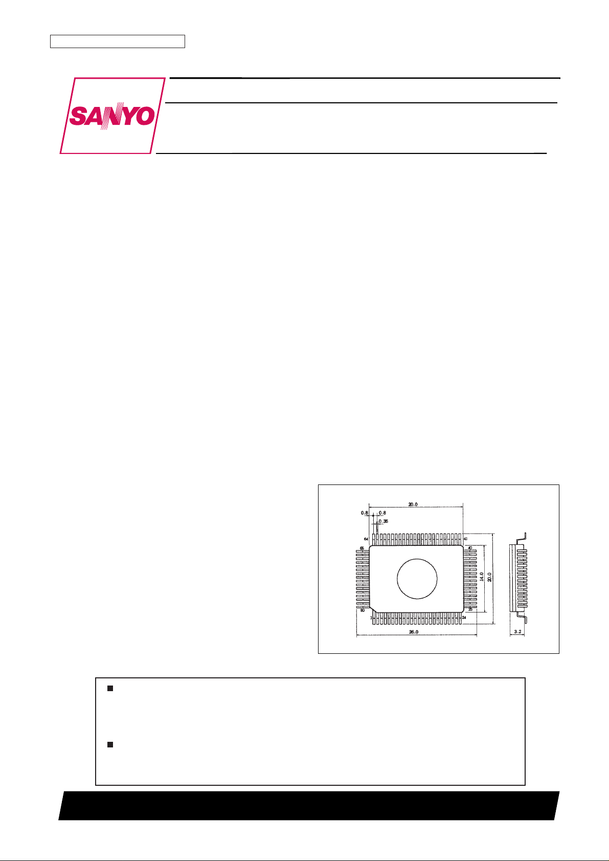
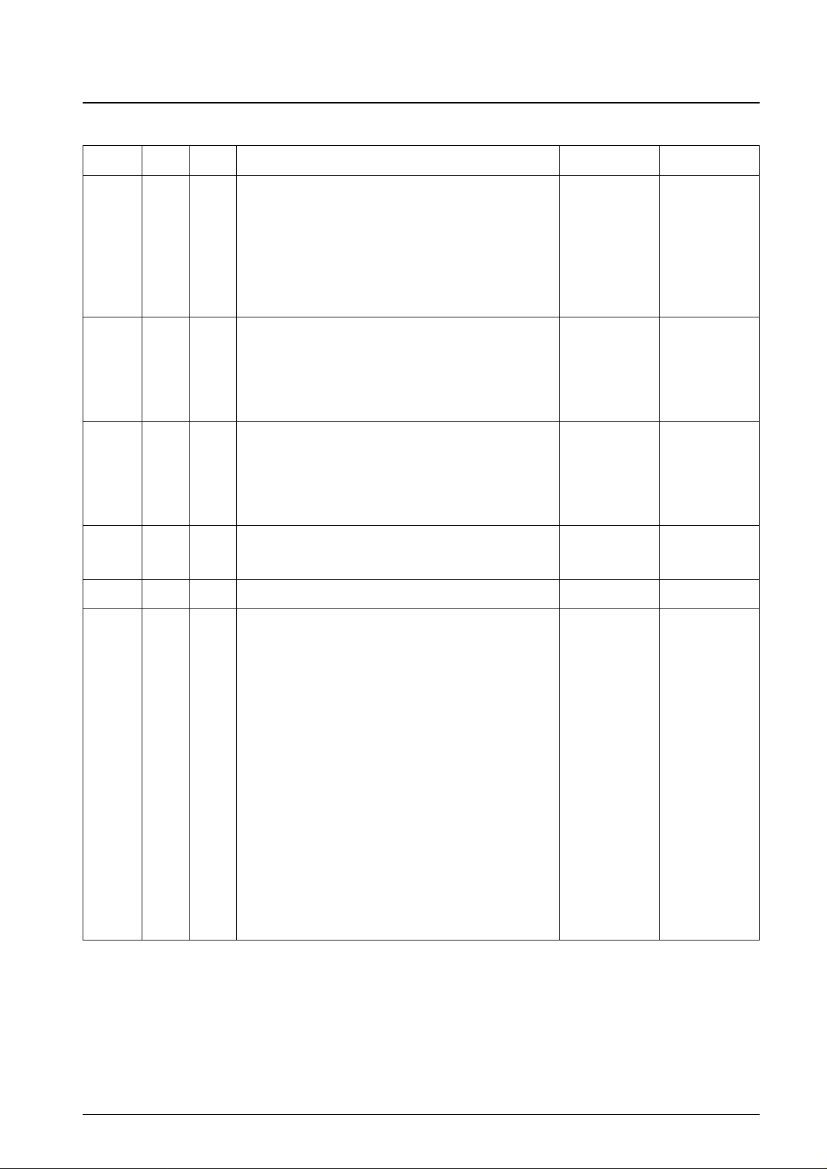
Package Dimensions
unit: mm
3152A-QFC80
[LC58E76]
SANYO: QFC80
Page 2
Series Structure
Usage Notes
The LC58E76 is designed for use in developing and evaluating programs for the microprocessors in the
LC587X series. However, there are differences between the LC58E76 and the mask ROM versions. Keep the
following points in mind when using the LC58E76.
1. Notes on Reset
When the RES pin input changes from high to low, the reset state is cleared after the prescribed oscillator
stabilization period has elapsed. The options and the segment PLA are set up during the first 256 cycles following the
clearing of the reset state. Instructions are executed starting at location 0 after this setup phase has completed. (The
options are undefined and the segment outputs are held at the VSSlevel when the RES pin is high and during the first
256 cycles following the clearing of the reset state.)
2. Cover the LC58E76’s window with an opaque seal when writing data to EPROM.
3. The LC58E76 and the mask ROM versions differ in the following points.
Note: Although the strobes number 00 to 1E can be used with CF 2 MHz and lower specifications, strobes number 0E, 0F and 1E cannot be used with the
CF 4 MHz specifications.
No. 4434-2/17
LC58E76
Type No.
LC5872 LC5873 LC5874 LC5876 LC58E76
Item
ROM capacity 2 k
× 16 bits 3 k × 16 bits 4 k × 16 bits 6 k × 16 bits EPROM: 16 kbytes
RAM capacity 256 × 4 bits 256 × 4 bits 256× 4 bits 256 × 4 bits 256 × 4 bits
Package QIP80 QIP80 QIP80 QIP80
QFC80 ceramic window
package
The on-chip EPROM
Notes Available in quantity Available in quantity Available in quantity Available in quantity window version will be
available shortly.
Item LC58E76 Mask ROM versions (LC587X) Note
Operating temperature 10 to 40°C –30 to 70°C
Operating supply voltage 2.8 to 5.5 V 2.0 to 6.0 V
5 µA typ. (3 V, 32 kHz crystal) 4 µA typ. (3 V, 32 kHz crystal)
20 µA typ. (5 V, 32 kHz crystal) 15 µA typ. (5 V, 32 kHz crystal)
Operating supply currents 400 µA typ. (5 V, 400 kHz ceramic) 400 µA typ. (5 V, 400 kHz ceramic) Hold mode
500 µA typ. (5 V, 2 MHz ceramic) 500 µA typ. (5 V, 2 MHz ceramic)
700 µA typ. (5 V, 4 MHz ceramic) 700 µA typ. (5 V, 4 MHz ceramic)
Common segment output Segment pins: VSS level (CMOS output) Static operation
states at reset Common pins: N-channel open drain (LCD drive output)
Segment output states
after the reset state is Off state Off state/lit state
cleared
Oscillator circuit
CF/Xtal/CF + Xtal
CF/Xtal/CF + Xtal
specifications RC/RC+Xtal/EXT/EXT+Xtal
Crystal oscillator circuit
32K/38K/65K (Note that this is 65K in the
32K/38K/65K
reset state)
Open (reset on high)
RES pin specifications Open (reset on high)
Open (reset on low)
Pull-up (reset on low)
Pull-down (reset on high)
N ports Open drain output Open drain output/CMOS output
Static Static
1/2 bias, 1/2 duty 1/2 bias, 1/2 duty
1/2 bias, 1/3 duty 1/2 bias, 1/3 duty
LCD drive specifications
1/2 bias, 1/4 duty 1/2 bias, 1/4 duty
1/3 bias, 1/3 duty 1/3 bias, 1/3 duty
1/3 bias, 1/4 duty 1/3 bias, 1/4 duty
(Substitute static when the LCD driver is not (Substitute static when the LCD driver is not
used.) used.)
Number of specifiable
00 – 1E 00 – 1E
However, 0E and 0F cannot be used with However, 0E and 0F cannot be used with
strobes
the 4 MHz specifications. the 4 MHz specifications.
• Option switching in the
EPROM version is
performed by writing
data to the option
EPROM.
• Option switching in
mask ROM versions is
performed by
specifying mask
options.
Page 3
Pin Assignments
Note: 1. The TST pin must be connected to VSSin normal operation.
2. When mounting the LC58E76, do not use solder dip techniques.
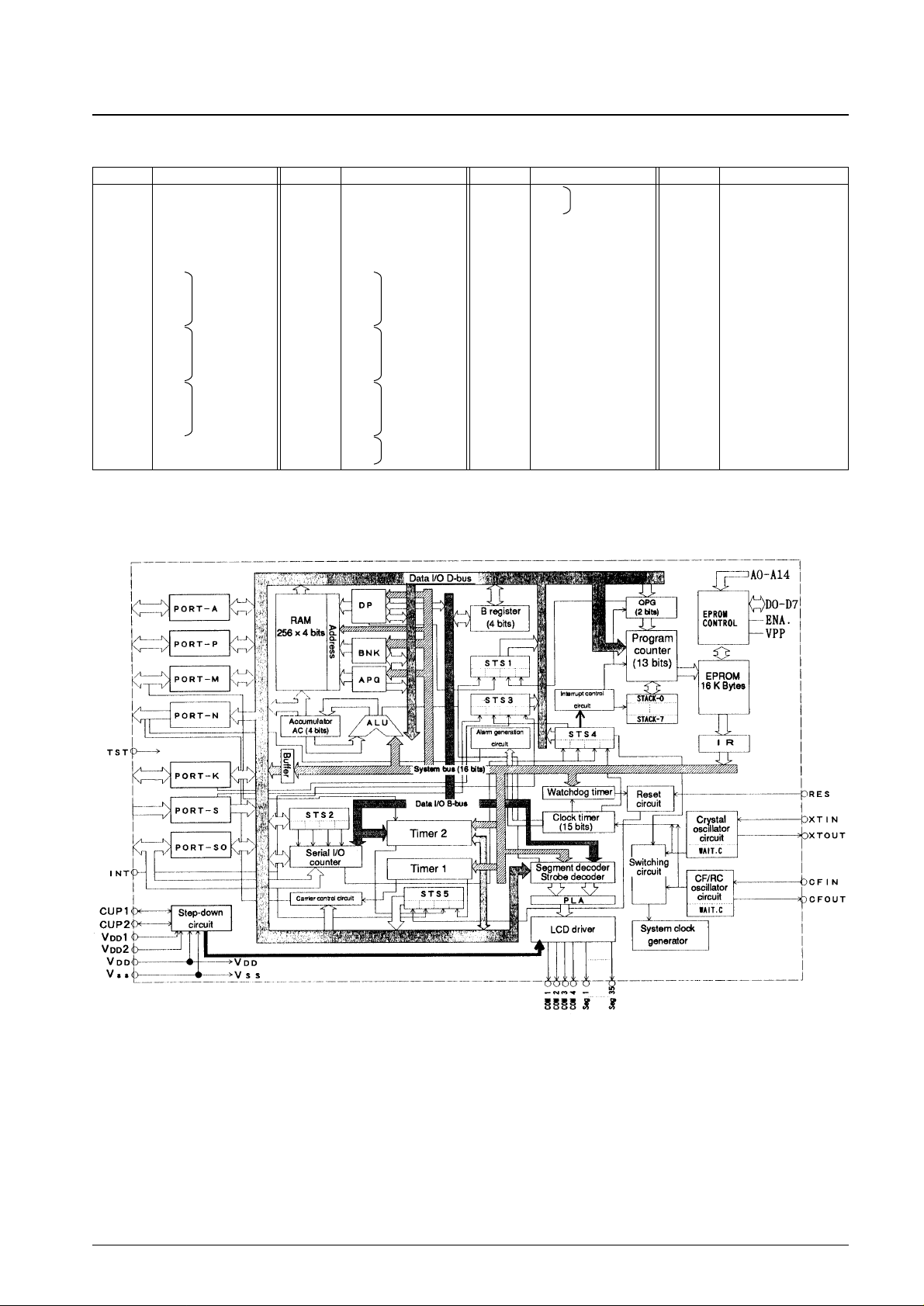
System Block Diagram
LC58E76 System Block Diagram
No. 4434-3/17
LC58E76
PIn No. Symbol PIn No. Symbol PIn No. Symbol PIn No. Symbol
1
2
3
4
5
6
7
8
9
10
11
12
13
14
15
16
17
18
19
20
COM2
COM1
CUP1
CUP2
RES
INT
SO1
SO2
SO3
SO4
A1
A2
A3
A4
P1
P2
P3
P4
XTOUT
XTIN
21
22
23
24
25
26
27
28
29
30
31
32
33
34
35
36
37
38
39
40
V
DD
2
V
DD
1
V
SS
V
DD
CFIN
CFOUT
S1
S2
S3
S4
K1
K2
K3
K4
M1
M2
M3
M4
N1
N2
41
42
43
44
45
46
47
48
49
50
51
52
53
54
55
56
57
58
59
60
N3
N4
TST
Seg1
Seg2
Seg3
Seg4
Seg5
Seg6
Seg7
Seg8
Seg9
Seg10
Seg11
Seg12
Seg13
Seg14
Seg15
Seg16
Seg17
61
62
63
64
65
66
67
68
69
70
71
72
73
74
75
76
77
78
79
80
Seg18
Seg19
Seg20
Seg21
Seg22
Seg23
Seg24
Seg25
Seg26
Seg27
Seg28
Seg29
Seg30
Seg31
Seg32
Seg33
Seg34
Seg35
COM4
COM3
I/O, serial I/O
ports
Input ports
Output ports
I/O ports
I/O ports
I/O ports
I/O ports
Output ports
RAM : Data memory
ROM : Program memory
DP : Data pointer register
BNK : Bank register
APG : RAM page flag
AC : Accumulator
ALU : Arithmetic and logic unit
B : B register
OPG : ROM page flag
PC : Program counter
IR : Instruction register
STS1 : Status register 1
STS2 : Status register 2
STS3 : Status register 3
STS4 : Status register 4
STS5 : Status register 5
PLA : Program logic for
segment data and strobes
WAIT.C : Wait time counter
Page 4
Pin Functions
No. 4434-4/17
LC58E76
Pin I/O
QFC-80
Function Option At reset
Pin No.
V
DD
— 24
V
SS
— 23
VDD1 — 22
V
DD
2 — 21
CUP1 — 3
CUP2 — 4
CFIN Input 25
CFOUT Output 26
XTIN Input 20
XTOUT Output 19
S1 27
S2 28
S3
Input
29
S4 30
K1 31
K2 32
K3
I/O
33
K4 34
M1 35
M2
I/O
36
M3 37
M4 38
A1 11
A2
I/O
12
A3 13
A4 14
P1 15
P2
I/O
16
P3 17
P4 18
Power supply
LCD drive power supply
Switching pin used to supply the LCD drive voltage to the VDD1 and
VDD2 pins
• Connect a nonpolar capacitor between CUP1 and CUP2 when 1/2 or
1/3 bias is used.
• Leave open when a bias other than 1/2 or 1/3 is used.
• CF specifications
• Not used
• The pull-up or pulldown resistors are
on.
Note: These pins go
to the floating
state when
reset is cleared.
• The pull-up or pulldown resistors are
on.
Note: These pins go
to the floating
state when
reset is cleared.
• Input mode
• Output latch data is
set high.
NON 1/1 bias 1/2 bias 1/3 bias
V
DD
VDD1
V
DD
2
V
SS
• 32k specifications
• 65k specifications
• 38k specifications
• Not used
• Transistors to hold
a low or high level
• Selection of either
pull-up or pulldown resistors
• Transistors to hold
a low or high level
• Selection of either
pull-up or pulldown resistors
The same as K1 toK4The same as K1 to
K4
The same as K1 to
K4
The same as K1 to
K4
The same as K1 to
K4
The same as K1 to
K4
System clock oscillator connections
• Ceramic resonator connection (CF specifications)
• RC component connection (RC specifications)
• External signal input pin (CFOUT is left open)
This oscillator is stopped by the execution of a STOP or SLOW
instruction.
Reference calculation (clock specifications, LCD alternation frequency),
system clock oscillator
• 32 kHz crystal resonator connection
• 65 kHz crystal resonator connection
This oscillator is stopped by the execution of a STOP instruction.
Input-only ports
• Input pins used to read data into RAM
• Built-in 7.8 ms and 1.95 ms chatter exclusion circuits
• Built-in pull-up/pull-down resistors
Note: The 7.8 ms and 1.95 ms times are the times when ø0 is
32.768 kHz.
I/O ports
• Input pins used to read data into RAM
• Output pins used to output data from RAM
• Built-in 7.8 ms and 1.95 ms input-mode chatter exclusion circuits. The
selection of 7.8 or 1.95 ms is linked to that for the S ports.
Note: The 7.8 ms and 1.95 ms times are the times when ø0 is
32.768 kHz.
I/O ports
• Input pins used to read data into RAM
• Output pins used to output data from RAM
• M4 is used as the external clock input pin in TM2 mode 3.
* The minimum period for the external clock is twice the cycle time.
• Built-in pull-up/pull-down resistors
I/O ports
• Input pins used to read data into RAM
• Output pins used to output data from RAM
• Built-in pull-up/pull-down resistors
I/O ports
Function: The same as pins A1 to A4
Continued on next page.
Page 5
Continued from preceding page.
No. 4434-5/17
LC58E76
Pin I/O
QFC-80
Function Option At reset
Pin No.
SO1 7
SO2
I/O
8
SO3 9
SO4 10
N1 39
N2
Output
40
N3 41
N4 42
INT Input 6
RES Input 5
TST Input 43
I/O ports
Function: The same as pins A1 to A4
Pins SO1 to SO3 area also used for the serial interface.
• Use of these pins in serial mode can be selected under program
control.
• Pin functions: SO1: Serial input pin
SO2: Serial output pin
SO3: Serial clock pin
The serial clock pin can be switched between internal and external,
and between rising edge output and falling edge output.
• Transistors to hold
a low or high level
• Selection of either
pull-up or pulldown resistors
• Internal serial clock
divisor selection
I 1/1
II 1/2
III 1/4
The same as K1 to
K4
The output levels on
pins N1 to N4 can be
specified as an option.
• Pin N1 to N4
output circuit type:
I N-channel
open drain
• Pin N1 to N4
output level
I High level
II Low level
• Transistors to hold
a low or high level
• Selection of either
pull-up or pulldown resistors
• Signal conversion
(rising/falling)
selection
* Only when the
input resistor open
specification is
selected
• LCD driver/
general-purpose
output switching
• LCD drive type
switching
— STATIC
— 1/2 bias – 1/2
duty
— 1/2 bias – 1/3
duty
— 1/2 bias – 1/4
duty
— 1/3 bias – 1/3
duty
— 1/3 bias – 1/4
duty
• General-purpose
output circuit
switching
— CMOS
— P-channel
open drain
— N-channel
open drain
• Output latch control
in standby modes
• LCD drive
All segments off
• General-purpose
outputs
Low level
Note: When a
combination of
LCD drive and
general- purpose outputs,
the output
state is either
all segments
off or low level.
• These pins go to
the V
SS
level
during the reset
period.
Output-only ports
• Output pins used to output data from RAM
• An alarm signal can be output from pin N4. (Note that this is only
when the N4 output latch is low.)
• An alarm signal modulated at 1, 2 or 4 kHz can be output. (These
frequencies are output when ø0 is 32.768 kHz.)
• A carrier signal can be output from N3. (Note that this is only when
the N3 output latch is low.)
Input ports
• External interrupt request inputs
• Input pins used to read data into RAM
• Input detection can be performed on either rising or falling edges.
• Built-in pull-up/pull-down resistors
LSI reset input
• The LC58E7008 resets on a high level input
Note: • An external resistor is required.
• The reset pulse must be at least 200 µs.
Test input
Connect to V
SS
in normal operation.
• LCD panel drive/general-purpose output
— LCD panel drive
I STATIC
II 1/2 bias – 1/2 duty
III 1/2 bias – 1/3 duty
IV 1/2 bias – 1/4 duty
V 1/3 bias – 1/3 duty
VI 1/3 bias – 1/4 duty
Types I to V can be specified as mask options.
— General-purpose output mode
I CMOS
II P-channel open drain
III N-channel open drain
Types I to III can be specified as mask options.
• LCD/general-purpose output control is handled by the segment PLA,
and thus program control is not required.
• These pins support output latch control on reset and in standby
states when the oscillators are stopped.
• Arbitrary combinations of LCD drive and general-purpose outputs can
be used.
Seg1,
Seg2 to
Seg35
Output
44,
45 to
78
Continued on next page.
Page 6
Continued from preceding page.
Usage Notes
The following tools and software are required when the LC58E76 is used.
The LC5870 Series Software Development Tools: For creating programs and option data.
Note that only MS-DOS machines are supported as the development host machine. See the LC5870 Series Software
Development Tools manuals for details on the use of these tools.
EC5876.EXE: This is a program that converts and merges program and option data for the LC5870 series so that it can
be written to the LC58E76 EPROM.
EPROM writing board (adapter socket: W58E68Q): This is a socket adapter that allows a general-purpose PROM writer
to be used to write program data to the LC58E76.
General-purpose PROM writer: The EVA-520 programmer that comes with the LC5870 Series Software Development
Tools cannot be used. A general-purpose PROM writer must be used.
This section describes the procedures used with the LC58E76 and the EC5876.EXE program, which is one of the tools
mentioned above. More details on LC5870 Series program development are available in LC5870 Series Users Manual
and the manuals for the LC5870 Series Development Tools and the general-purpose PROM writer.
No. 4434-6/17
LC58E76
Pin I/O
QFC-80
Function Option At reset
Pin No.
COM1 2
COM2 1
COM3
Output
80
COM4 79
These pins are nchannel open-drain
outputs during the
reset period.
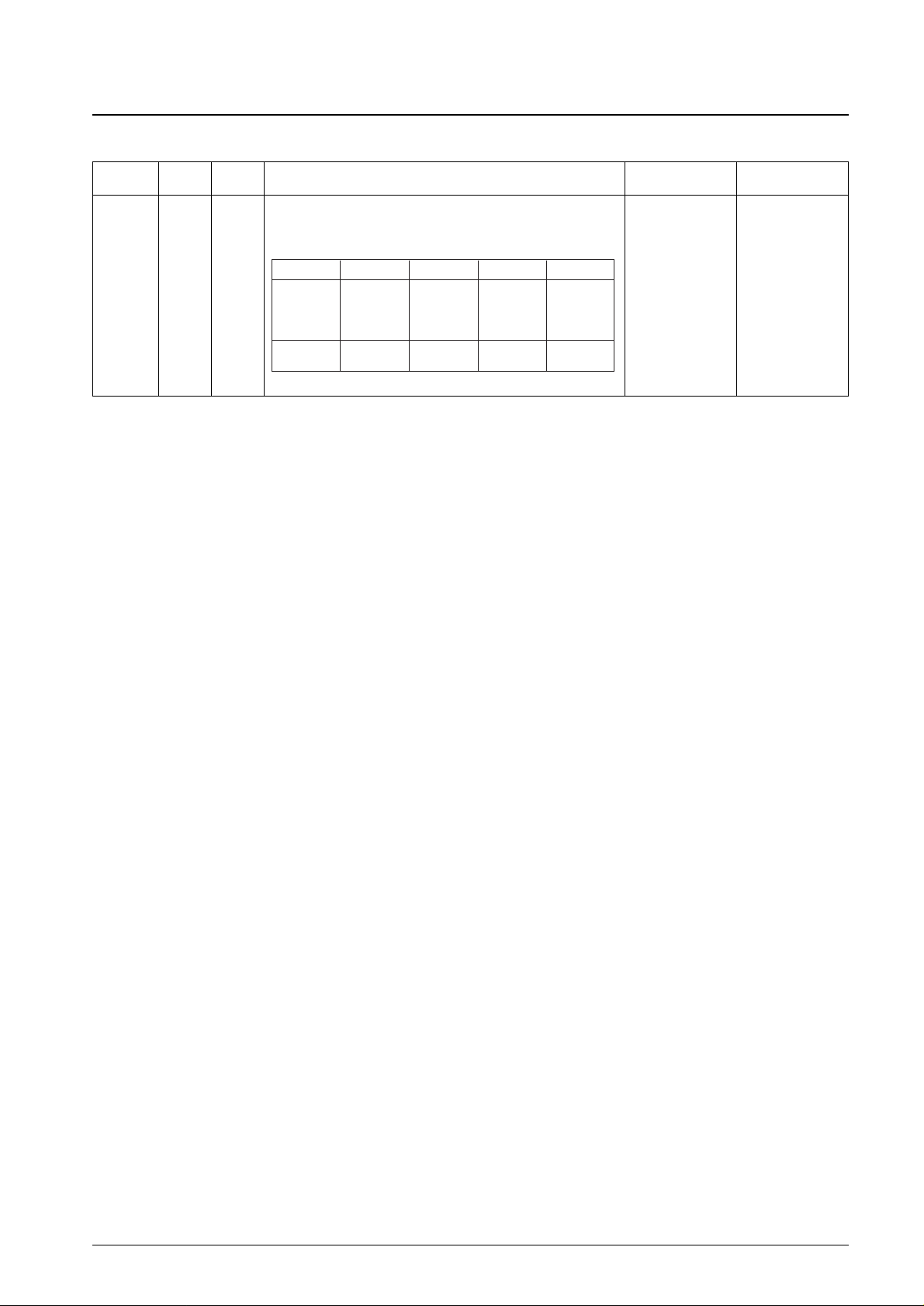
LCD panel drive common polarity outputs
The table below shows how these pins are used depending on the duty
used. (Values for alternation frequency reflect a typical specification of
32.768 MHz for ø0)
Note: A cross ( × ) indicates that the pin is not used with that duty type.
Static duty 1/2 duty 1/3 duty 1/4 duty
COM1
❍ ❍ ❍ ❍
COM2
× ❍ ❍ ❍
COM3
× × ❍ ❍
COM4
× × × ❍
Alternation
32 Hz 32 Hz 42.7 Hz 32 Hz
frequency
Page 7

1. Procedure (This flowchart describes the procedure used.)
Note: There are differences in function and characteristics between the LC58E76 and the LC5870 series mask ROM
versions. Be sure to take these differences into account when testing the programmed LC58E76. See the “Usage
Notes” section for details on the differences.
2. Using the EC5876.EXE Program (Operation)
As shown in the figures below, the data to be written to the LC58E76 consists of a program data area (instruction
code area) and an option data area. The EC5876.EXE program applies a special conversion process to the option
specification data to create the option data area data.
The EC5876.EXE program converts and merges program data and option data to create the data to be written to the
LC58E76.
• Start-up procedure
A:>EC5876 ROMSAMP.HEX PLASAMP.HEX EP-SAMP.HEX<ENT>
Or:
A:>EC5876<ENT>
*******************************************************
* LC58E76 PROGRAM & MASK OPTION CONVERSION Ver XXXXXX *
*******************************************************
ROM PROGRAM NAME : ROMSAMP.HEX<ENT>
PLA PROGRAM NAME : PLASAMP.HEX<ENT>
EP ROM WRITE NAME: EP–SAMP.HEX<ENT>
Program complete...........Program termination message
No. 4434-7/17
LC58E76
Specification
determination
Mask option
specification
Program creation and
debugging
Data conversion and
merging for the
LC58E76
PROM writer setup
Write data transfer
EPROM writing
board setup
Write
Mounted configuration
program testing
Use the SU5870.EXE program to create the option specification data.
Use the LC5870S.EXE cross assembler to create the program. Use the dedicated development tools
for debugging.
Use the EC5876.EXE program to convert and merge the program and option data. This creates the
data to be written to the LC58E76 EPROM. (See “Using the EC5876.EXE Program”.)
Setup the PROM writer ROM type, the start and stop addresses, and other states.
(See “Use of the EPROM Writing Board”.)
Transfer the LC58E76 EPROM data created with the EC5876.EXE program to the PROM writer.
Mount the PROM writer in the LC58E76 EPROM writing board.
Mount the LC58E76 in the EPROM writing board, and write the data.
Apply an opaque seal to the LC58E76 window at the point that the data is written.
Mount the LC58E76 in the socket in the application circuit, and check that the program functions
correctly.
Page 8

• Error messages
Error ON filename.HEX, FILE NOT FOUND...............The file “filename.HEX” was not found.
The filename “filename.HEX” was incorrect.
Error ON MAKE LC5876, 5874, 5873, 5872.............The ROM data and the option data object
microprocessor type did not agree. The ROM data
must be created with a cross assembler and option
specification software designed for the same
microprocessor type.
Error ON filename.HEX, EOF NOT DETECTED..........A hexadecimal record end marker was not found
in the file “filename.HEX”.
Error ON filename.HEX, ILLEGAL CHARACTER........A character other than 0 to 9 or A to F was found
in a hexadecimal context while reading the file
“filename.HEX”.
Error ON filename.HEX, ADDRESS OVER....................An address in the file “filename.HEX” exceeded
the allowed range.
Error ON filename.HEX, ILLEGAL FILEHDR.............The header in the file “filename.HEX” is not for
the LC5870 series.
There was an error in the hexadecimal file
specification.
Error ON command line input,
INVALID NUMBER OF PARAMETERS...............The number of parameters in the command line
was inappropriate.
Error ON ILLEGAL, MASK OPTION DATA......................There was an error in the mask option data.
• EPROM data structure
Cross assembler and mask option data EPROM Data
(1) Cross assembler data
(2) Mask option data
No. 4434-8/17
LC58E76
Page 9

3. Use of the W58E68Q EPROM Writing Board (Board used with both the LC58E68 and the LC58E76)
The EPROM writing board is a socket adapter that fits the LC58E76 to the device socket in a general-purpose
PROM writer.
• EPROM Writing Board Appearance
• PROM writer settings
— ROM type: 256 K, VPP = 21 V mode
— Start and stop addresses: Set these to 0000H and 40FFH.
4. Erasing LC58E76 EPROM Data
Use a general-purpose EPROM eraser to erase data written to an LC58E76.
5. Notes On Order Mask ROM
• The following methods cannot be used to order LC5870 Series mask ROM products.
— Use of “.HEX” files that were converted and merged for use in an LC58E76
— Use of an LC58E76 itself
• Ordering mask ROM
— Use the program hexadecimal data generated by the cross assembler.
— Use the option hexadecimal data generated by the option specification software.
— Provide three EPROMs to which the program hexadecimal data has been written using a general-purpose
EPROM writer.
— Provide three EPROMs to which the option hexadecimal data has been written using a general-purpose
EPROM writer.
No. 4434-9/17
LC58E76
Page 10

Specifications
The electrical characteristics listed here are provisional values and are subject to change.
Absolute Maximum Ratings at VSS= 0 V, TA = 25°C
No. 4434-10/17
LC58E76
Parameter Symbol Conditions/Pin
Ratings
Unit
min typ max
V
DD
–0.3 +6.0 V
Maximum supply voltage V
DD
1 –0.3 V
DD
V
V
DD
2 –0.3 V
DD
V
V
I
(1)
As allowed in the specified circuit (Figure 1)
Allowed up to the voltage that appears
XTIN, CFIN
Maximum input voltage S1 – 4, K1 – 4, P1 – 4, SO1 – 4, A1 – 4, RES,
V
DD
VI(2) INT, TST –0.3
+0.3
V
(K, P, M, SO and A ports in input mode)
V
O
(1)
As allowed in the specified circuit (Figure 1)
Allowed up to the voltage that appears
XTOUT, CFOUT
K1 –4, P1 – 4, SO1 – 4, A1 – 4, N1 – 4,
V
DD
Maximum output voltage VO(2) CUP1, CUP2, Seg1 – 35, COM1 – 4, –0.3
+0.3
V
(K, P, M, SO and A ports in output mode)
V
O
(3) Open drain specifications
N1 to N4
–0.3 +13 V
(n-channel)
I
O
(1) Per pin
N1 – 4
0 15 mA
I
O
(2) Per pin –10 0 mA
I
O
(3) Per pin
K1 – 4, P1 – 4, M1 – 4, SO1 – 4, 0 5 mA
Output pin current
I
O
(4) Per pin
A1 – 4 –5 0 mA
Σ I
O
(1)
Total (summed)
K1 – 4, P1 – 4, M1 – 4, 70 mA
pin current
SO1 – 4, A1 –4, N1 – 4,
Σ IO(2)
Total (summed)
Seg1 – 35
–70 mA
pin current
Allowable power dissipation Pdmax For the QFC80 window ceramic flat package 500 mW
Operating temperature Topr 10 40 °C
Storage temperature Tstg –55 +125 °C
Page 11

Allowable Operating Ranges at VSS= 0 V, Ta = 25°C
Note: * In a state with the CF/RC oscillator and the crystal oscillator completely stopped, and all internal circuits stopped
Electrical Characteristics at VDD= 2.8 to 3.2 V, VSS= 0 V, Ta = 25°C
Note: * The 24 pins S1 to S4, K1 to K4, P1 to P4, M1 to M4, SO1 to SO4 and A1 to A4.
No. 4434-11/17
LC58E76
Parameter Symbol Conditions/Pin
Ratings
Unit
min typ max
No LCD specifications: V
DD
1 = VDD2 = V
DD
2.8 5.5 V
Static drive specifications: V
DD
1 = VDD2 = V
DD
2.8 5.5 V
Supply voltage V
DD
1/2 bias specifications: VDD1 = VDD2 ≅ 1/2V
DD
2.8 5.5 V
1/3 bias specifications: V
DD
1 ≅ 2 × 1/3V
DD
2.8 5.5 V
V
DD
2 ≅ 1/3V
DD
Data retention supply voltage V
HD
RAM and register contents retention voltage* 2.8 V
DD
V
S1 – 4, K1 – 4, P1 – 4, M1 – 4, SO1 – 4,
Input high-level voltage VIH1
A1 – 4, INT
0.7 V
DD
V
DD
V
(K, P, M, SO and A ports in input mode)
Input low-level voltage VIL1 0 0.3 V
DD
V
Input high-level voltage V
IH
2
RES pin
0.75 V
DD
V
DD
V
Input low-level voltage V
IL
2 0 0.25 V
DD
V
Input high-level voltage V
IH
3
CFIN pin
0.75 V
DD
V
DD
V
Input low-level voltage V
IL
3 0 0.25 V
DD
V
Operating frequency 1 fopg1 V
DD
= 2.8 to 5.5 V, 32 kHz
XTIN/XTOUT
32 33 kHz
Operating frequency 2 fopg2 V
DD
= 2.8 to 5.5 V, 38 kHz crystal 37 39 kHz
Operating frequency 3 fopg3 V
DD
= 2.8 to 5.5 V, 65 kHz
oscillator
60 70 kHz
Operating frequency 4 fopg4 V
DD
= 2.8 to 5.5 V
CFIN/CFOUT CF
190 1200 kHz
Operating frequency 5 fopg5 V
DD
= 3.0 to 5.5 V 190 2300 kHz
Operating frequency 6 fopg6 V
DD
= 4.5 to 5.5 V
specifications
190 4200 kHz
Pins SO1 and SO3
(in serial mode)
Operating frequency 7 fopg7 V
DD
= 3.0 to 5.5 V
The rising and falling
DC 200 kHz
edges of input signal
and clock waveforms
must be ≤ 10 µs.
Parameter Symbol Conditions/Pin
Ratings
Unit
min typ max
R
IN
1 A
VIN = 0.2 V
DD
,
60 300 1200 kΩ
Low-level hold transistor *, Figure 2
RIN1 B VIN = VDD, Pull-down resistor *, Figure 2 30 150 500 kΩ
R
IN
1 C
VIN = 0.8 V
DD
,
60 300 1200 kΩ
High-level hold transistor *, Figure 2
Input resistance
RIN1 D VIN = VSS, Pull-up resistor *, Figure 2 30 150 500 kΩ
R
IN
2 A VIN = 0.2 VDD, INT low-level hold transistor 60 300 1200 kΩ
R
IN
2 B VIN = VDD, INT pull-down resistor 300 1500 5000 kΩ
R
IN
2 C VIN = 0.8 VDD, INT high-level hold transistor 60 300 1200 kΩ
R
IN
2 D VIN = VSS, INT pull-up resistor 300 1500 5000 kΩ
R
IN
3
VIN = V
DD
,
20 70 300 kΩ
With a pull-down resistor on the TST pin
Output low-level voltage VOL(1) IOL = 1.0 mA N1 – 4 0.5 V
Output high-level voltage V
OH
(2) IOH = –400 µA
K1 – 4, P1 – 4, M1 – 4,
V
DD
– 0.5 V
SO1 – 4, A1 – 4
Output low-level voltage V
OL
(2) IOL = 400 µA
(K, P, M, SO and A ports
0.5 V
in output mode)
Output off leakage current | I
OFF
| VOH = 10.5 V N1 – 4, Figure 10 1.0 µA
Segment port output impedance
• When CMOS output ports are used
Output high-level voltage V
OH
(3) IOH = –100 µA
Seg 1 to 35
VDD– 0.5 V
Output low-level voltage V
OL
(3) IOL = 100 µA 0.5 V
Continued on next page.
Page 12

Continued from preceding page.
No. 4434-12/17
LC58E76
Parameter Symbol Conditions/Pin
Ratings
Unit
min typ max
• When p-channel open-drain output ports are used (See Figure 11.)
Output high-level voltage V
OH
(3) IOH= –100 µA
Seg 1 to 35
VDD– 0.5 V
Output off leakage current | I
OFF
| VOL= V
SS
1.0 µA
• When n-channel open-drain output ports are used (See Figure 11.)
Output low-level voltage V
OL
(3) IOL= 100 µA
Seg 1 to 35
0.5 V
Output off leakage current | I
OFF
| VOH= V
DD
1.0 µA
• Static drive
Output high-level voltage V
OH
(4) IOH= –20 µA Seg 1 to 35 VDD– 0.2 V
Output low-level voltage V
OL
(4) IOL= 20 µA 0.2 V
Output high-level voltage V
OH
(5) IOH= –100 µA COM1 VDD– 0.2 V
Output low-level voltage V
OL
(5) IOL= 100 µA 0.2 V
• 1/2 bias
Output high-level voltage V
OH
(4) IOH= –20 µA
Seg 1 to 35
VDD– 0.2 V
Output low-level voltage V
OL
(4) IOL= 20 µA 0.2 V
Output high-level voltage V
OH
(6) IOH= –100 µA VDD– 0.2 V
Output middle-level voltage V
OM
2–1
I
OH
= –100 µA
COM1 – 4 V
DD
/2 – 0.2 VDD/2 + 0.2 V
I
OL
= 100 µA
Output low-level voltage V
OL
(6) IOL= 100 µA 0.2 V
• 1/3 bias
Output high-level voltage V
OH
(4) IOH= –20 µA VDD– 0.2 V
Output middle-level voltage
V
OM
1–1
I
OH
= –20 µA
Seg 1 to 35
2V
DD
/3 – 0.2 2VDD/3 + 0.2 V
V
OM
1–2
I
OL
= 20 µA
V
DD
/3 – 0.2 VDD/3 + 0.2 V
Output low-level voltage V
OL
(4) IOL= 20 µA 0.2 V
Supply leakage current I
LEK
(1) VDD= 3.0 V
Ta = 25°C, STOP mode,
1.0 µA
Figure 3
VDD= 3.0 V
Input leakage current I
OFF
VIN= V
DD
1.0 µA
V
IN
= V
SS
–1.0 µA
VDD= 3.0 V, C1 = C2 = 0.1 µF
Output voltage 1 V
DD
1–(1) 1/2 bias, fopg = 32.768 kHz, VDD1 = V0 1.5 V
Figure 4
V
DD
2–(1)
V
DD
= 3.0 V, C1 = C2 = 0.1 µF
V
DD
1 = V0
2.0 V
Output voltage 2
V
DD
2–(2)
1/3 bias, fopg = 32.768 kHz,
V
DD
2 = V0
1.0 V
Figure 4
Ta = 25°C, Crystal oscillator
specifications, Crystal: 32 kHz,
Supply current 1 | I
DD
| 1 V
DD
DD
= 3.0 V Cg = 20 pF, CI = 25 kΩ 5.0 µA
Halt mode, LCD at 1/3 bias,
Figure 6
Ta = 25°C, Crystal oscillator
specifications, Crystal: 38 kHz
Supply current 2 | I
DD
| 2 VDD= 3.0 V or 65 kHz, Cg = 10 pF, 10.0 µA
CI = 25 kΩ, Halt mode,
LCD at 1/3 bias, Figure 6
Ta = 25°C, CF oscillator
specifications, CF: 400 kHz,
Supply current 3 | I
DD
| 3 VDD= 3.0 V Ccg = Ccd = 330 pF 150 µA
Halt mode, LCD at 1/3 bias,
Figure 8
Ta = 25°C, CF oscillator
Supply current 4 | I
DD
| 4 VDD= 3.0 V
specifications, CF: 1 MHz,
200 µA
Ccg = Ccd = 100 pF, Halt mode,
LCD at 1/3 bias, Figure 8
S1 – 4, K1 – 4, P1 – 4,
M1 – 4, SO1 – 4, A1 – 4,
INT, RES (K, P, M, SO
and A ports in input
mode, INT and RES pin
open specifications)
Continued on next page.
Page 13

Continued from preceding page.
Electrical Characteristics at VDD= 4.5 to 5.5 V, VSS= 0 V, Ta = 25°C
Note: * The 24 pins S1 to S4, K1 to K4, P1 to P4, M1 to M4, SO1 to SO4 and A1 to A4.
No. 4434-13/17
LC58E76
Parameter Symbol Conditions/Pin
Ratings
Unit
min typ max
V
DD
= 2.8 V Crystal oscillator specifications,
Oscillator start time | TSTT | with a 32 kHz crystal 5 s
CI ≤ 25 kΩ, Cg = 20 pF
Oscillator stabilization degree ∆f
V
DD
= 2.95
Figure 6 3 ppm
to 3.05 V
Crystal oscillator specifications,
Oscillator start time | TSTT | V
DD
= 2.8 V
with a 38 or 65 kHz crystal
5 s
XCg = 10 pF, CI ≤ 25 kΩ
Figure 6
CF oscillator specifications,
Oscillator start time | TSTT | V
DD
= 2.8 V with a 400 kHz CF used 30 ms
Ccg = Ccd = 330 pF, Figure 7
CF oscillator specifications,
Oscillator start time | TSTT | V
DD
= 2.8 V
with an 800 kHz CF used
30 ms
Ccg = Ccd = 220 pF or 100 pF
Figure 7
Oscillator compensation
Cd V
DD
= 3.0 V XTOUT pin (built-in) 20 pF
capacitance
Parameter Symbol Conditions/Pin
Ratings
Unit
min typ max
R
IN
1 A
VIN = 0.2 V
DD
,
30 120 500 kΩ
Low-level hold transistor *, Figure 2
RIN1 B VIN = VDD, Pull-down resistor *, Figure 2 10 50 200 kΩ
R
IN
1 C
VIN = 0.8 V
DD
,
30 120 500 kΩ
High-level hold transistor *, Figure 2
Input resistance
RIN1 D VIN = VSS, Pull-up resistor *, Figure 2 10 50 200 kΩ
R
IN
2 A VIN = 0.2 VDD, INT low-level hold transistor 30 120 500 kΩ
R
IN
2 B VIN = VDD, INT pull-down resistor 100 500 2000 kΩ
R
IN
2 C VIN = 0.8 VDD, INT high-level hold transistor 30 120 500 kΩ
R
IN
2 D VIN = VSS, INT pull-up resistor 100 500 2000 kΩ
R
IN
3
VIN = V
DD
,
20 70 300 kΩ
With a pull-down resistor on the TST pin
Output low-level voltage VOL(1) IOL = 10.0 mA N1 – 4 0.5 V
Output high-level voltage V
OH
(2) IOH = –1.0 mA
K1 – 4, P1 – 4, M1 – 4,
V
DD
– 0.5 VDD– 0.2 V
SO1 – 4, A1 – 4
Output low-level voltage V
OL
(2) IOL = 2.0 mA
(K, P, M, SO and A ports
0.2
0.5 V
in output mode)
Output off leakage current | I
OFF
| VOH = 10.5 V N1 – 4, Figure 10 1.0 µA
Segment port output impedance
• When CMOS output ports are used
Output high-level voltage V
OH
(3) IOH = –500 µA
Seg 1 to 35
VDD– 0.5 VDD– 0.2 V
Output low-level voltage V
OL
(3) IOL = 500 µA 0.5 V
• When p-channel open drain output ports are used (See Figure 11.)
Output high-level voltage V
OH
(4) IOH = –500 µA
Seg 1 to 35
VDD– 0.5 VDD– 0.2 V
Output off leakage current | I
OFF
| VOL = V
SS
1.0 µA
• When n-channel open-drain output ports are used (See Figure 11.)
Output low-level voltage V
OL
(4) IOL = 500 µA
Seg 1 to 35
0.2 0.5 V
Output off leakage current | I
OFF
| VOH = V
DD
1.0 µA
• Static drive
Output high-level voltage V
OH
(4) IOH = –40 µA
Seg 1 to 35
VDD– 0.2 V
Output low-level voltage V
OL
(4) IOL = 40 µA 0.2 V
Output high-level voltage V
OH
(6) IOH = –400 µA
COM1
VDD– 0.2 V
Output low-level voltage V
OL
(6) IOL = 400 µA 0.2 V
Continued on next page.
Page 14

Continued from preceding page.
No. 4434-14/17
LC58E76
Parameter Symbol Conditions/Pin
Ratings
Unit
min typ max
• 1/2 bias
Output high-level voltage V
OH
(4) IOH= –40 µA
Seg 1 to 35
VDD– 0.2 V
Output low-level voltage V
OL
(4) IOL= 40 µA 0.2 V
Output high-level voltage V
OH
(6) IOH= –400 µA VDD– 0.2 V
Output middle-level voltage V
OM
2–1
I
OH
= –400 µA
COM1 – 4 V
DD
/2 – 0.2 VDD/2 + 0.2 V
I
OL
= 400 µA
Output low-level voltage V
OL
(6) IOL= 400 µA 0.2 V
• 1/3 bias
Output high-level voltage V
OH
(4) IOH= –40 µA VDD– 0.2 V
Output middle-level voltage
V
OM
1–1 IOH= –40 µA
Seg 1 to 35
2VDD/3 – 0.2 2VDD/3 + 0.2 V
V
OM
1–2
I
OL
= 40 µA
V
DD
/3 – 0.2 VDD/3 + 0.2 V
Output low-level voltage V
OL
(4)
I
OL
= 40 µA
0.2 V
Output high-level voltage V
OH
(6) IOH= –400 µA VDD– 0.2 V
Output middle-level voltage
V
OM
2–1
I
OH
= –400 µA
COM1 – 4
2V
DD
/3 – 0.2 2VDD/3 + 0.2 V
V
OM
2–2
I
OL
= 400 µA
V
DD
/3 – 0.2 VDD/3 + 0.2 V
Output low-level voltage V
OL
(6) IOL= 400 µA 0.2 V
Supply leakage current I
LEK
(1) VDD= 5.5 V
Ta = 25°C, Stop mode,
1.0 µA
Figure 3
VDD= 5.5 V
Input leakage current I
OFF
VIN= V
DD
1.0 µA
V
IN
= V
SS
–1.0 µA
Output voltage 1 V
DD
1–(1)
V
DD
= 5.0 V, C1 = C2 = 0.1 µF, VDD1 = V0
2.5 V
1/2 bias, fopg = 32.768 kHz Figure 4
V
DD
2–(1)
V
DD
= 5.0 V, C1 = C2 = 0.1 µF,
V
DD
1 = V0
3.33 V
Output voltage 2
V
DD
2–(2)
1/3 bias, fopg = 32.768 kHz
V
DD
2 = V0
1.67 V
Figure 4
Ta = 25°C, Crystal oscillator
specifications, Crystal: 32 kHz,
Supply current 1 | I
DD
| 1 V
DD
DD
= 5.0 V Cg = 20 pF, CI = 25 kΩ 20 µA
Halt mode, LCD at 1/3 bias,
Figure 6
Ta = 25°C, Crystal oscillator
specifications, Crystal: 38 kHz
Supply current 2 | I
DD
| 2 VDD= 5.0 V or 65 kHz, Cg = 10 pF, 30 µA
CI = 25 kΩ, Halt mode, LCD
at 1/3 bias, Figure 6
Ta = 25°C, CF oscillator
specifications, CF: 400 kHz,
Supply current 3 | I
DD
| 3 VDD= 5.0 V Ccg = Ccd = 330 pF 400 µA
Halt mode, LCD at 1/3 bias,
Figure 7
Ta = 25°C, CF oscillator
Supply current 4 | I
DD
| 4 VDD= 5.0 V
specifications, CF: 1 MHz,
450 µA
Ccg = Ccd = 100 pF, Halt mode,
LCD at 1/3 bias, Figure 8
Ta = 25°C, CF oscillator
Supply current 5 | I
DD
| 5-1 VDD= 5.0 V
specifications, CF: 2 MHZ,
500 µA
Ccg = Ccd = 33 pF, Halt mode,
LCD at 1/3 bias, Figure 8
Ta = 25°C, CF oscillator
Supply current 6 | I
DD
| 6-1 VDD= 5.0 V
specifications, CF: 4 MHz,
700 µA
Ccg = Ccd = 33 pF, Halt mode,
LCD at 1/3 bias, Figure 8
Oscillator compensation
Cd V
DD
= 5.0 V XTOUT pin (built-in) 20 pF
capacitance
S1 – 4, K1 – 4, M1 – 4,
SO1 – 4, A1 – 4, INT,
RES (K, P, M, SO and A
ports in input mode, INT
and RES pin open
specifications)
Page 15

Figure 1-(1) Specified Oscillator Circuit (XT pin) Figure 1-(2) Specified Oscillator Circuit (CF pin)
Figure 2 S, K, P, M, SO and A Port Input Circuit
(Reference)
Recommended Ceramic Resonators for Mask ROM Versions
No. 4434-15/17
LC58E76
Xtal
32 k: 32.768 kHz
65 k: 65.536 kHz
38 k: 38.2293 kHz
Manufacturer Murata Mfg. Co., Ltd. Kyocera Corporation
Item
Type No. Ccg (pF) Ccd (pF) Type No. Ccg (pF) Ccd (pF)
Frequency
400 kHz CSB400P 330 330 KBR-400B 330 330
800 kHZ CSB800J 220 220 KBR-800H 100 100
1 MHz CSB1000J 220 220 KBR-1000H 100 100
2 MHz CSA2.00MG, CST2.00MG 33 33 KBR-2.00MS 33 33
4 MHz CSA4.00MG, CST4.00MG 33 33 KBR-4.00MS 33 33
Figure 13 Serial I/O Timing
(in external clock mode)
Figure 14 Timer 2 External Clock Input Timing
(in external clock mode: pin M4)
Page 16

Figure 3 Supply Leakage Current Test Circuit
Figure 4 Output Voltage Test Circuit
Figure 6: Supply Current Test Circuit
Figure 8 Supply Current Test Circuit
Figure 3
• In the stop state
• With the S-port input resistors on
• With the I/O ports in output mode with high-level data
values
• With the INT pin built-in resistor connected and in the
open state
• With an external pull-down resistor on the RES pin
• The LCD-port values do not include the external
component currents.
• With a crystal frequency between 32 and 65 kHz
• With CF between 200 kHz and 4 MHz
Figures 4 and 5
• With a crystal frequency of 32 kHz
• C1, C2, and C3 are 0.1 µF capacitors.
• With the LCD ports open
• With CD between 200 kHz and 4 MHz
Figure 5 Output Voltage Test Circuit
Figure 7: Supply Current Test Circuit
Figure 10 Pin N1 to Pin N4 Circuits
No. 4434-16/17
LC58E76
Page 17

PS No. 4434-17/17
LC58E76
This catalog provides information as of December, 1998. Specifications and information herein are
subject to change without notice.
Specifications of any and all SANYO products described or contained herein stipulate the performance,
characteristics, and functions of the described products in the independent state, and are not guarantees
of the performance, characteristics, and functions of the described products as mounted in the customer’s
products or equipment. To verify symptoms and states that cannot be evaluated in an independent device,
the customer should always evaluate and test devices mounted in the customer’s products or equipment.
SANYO Electric Co., Ltd. strives to supply high-quality high-reliability products. However, any and all
semiconductor products fail with some probability. It is possible that these probabilistic failures could
give rise to accidents or events that could endanger human lives, that could give rise to smoke or fire,
or that could cause damage to other property. When designing equipment, adopt safety measures so
that these kinds of accidents or events cannot occur. Such measures include but are not limited to protective
circuits and error prevention circuits for safe design, redundant design, and structural design.
In the event that any or all SANYO products (including technical data, services) described or contained
herein are controlled under any of applicable local export control laws and regulations, such products must
not be exported without obtaining the export license from the authorities concerned in accordance with the
above law.
No part of this publication may be reproduced or transmitted in any form or by any means, electronic or
mechanical, including photocopying and recording, or any information storage or retrieval system,
or otherwise, without the prior written permission of SANYO Electric Co., Ltd.
Any and all information described or contained herein are subject to change without notice due to
product/technology improvement, etc. When designing equipment, refer to the “Delivery Specification”
for the SANYO product that you intend to use.
Information (including circuit diagrams and circuit parameters) herein is for example only; it is not
guaranteed for volume production. SANYO believes information herein is accurate and reliable, but
no guarantees are made or implied regarding its use or any infringements of intellectual property rights
or other rights of third parties.
Figure 11: Segment Pin Open-Drain Circuits
 Loading...