

Page 1
Ordering number : EN 4365B
O3095HA (OT)/91994TH (OT) No. 4365-1/29
Overview
The LC5852N is a high-performance four-bit single-chip
built-in LCD driver microprocessor that provides a variety
of attractive features including low-voltage operation and
low power dissipation. The LC5852N was developed as an
upwardly compatible version of the LC5851N and
provides a ROM capacity increased from 1024 to 2048 15bit words and a RAM capacity increased from 64 × 4 bits
to 128 × 4 bits.
Applications
• System control and LCD display in cameras, radios and
similar products
• System control and LCD display in miniature electronic
test equipment and consumer health maintenance
products
• The LC5852N is optimal for end products with LCD
displays and, in particular, for battery operated products.
Features
The LC5852N is an upwardly compatible version of the
LC5851N and, as such, has the following features.
• Extremely broad allowable operating ranges
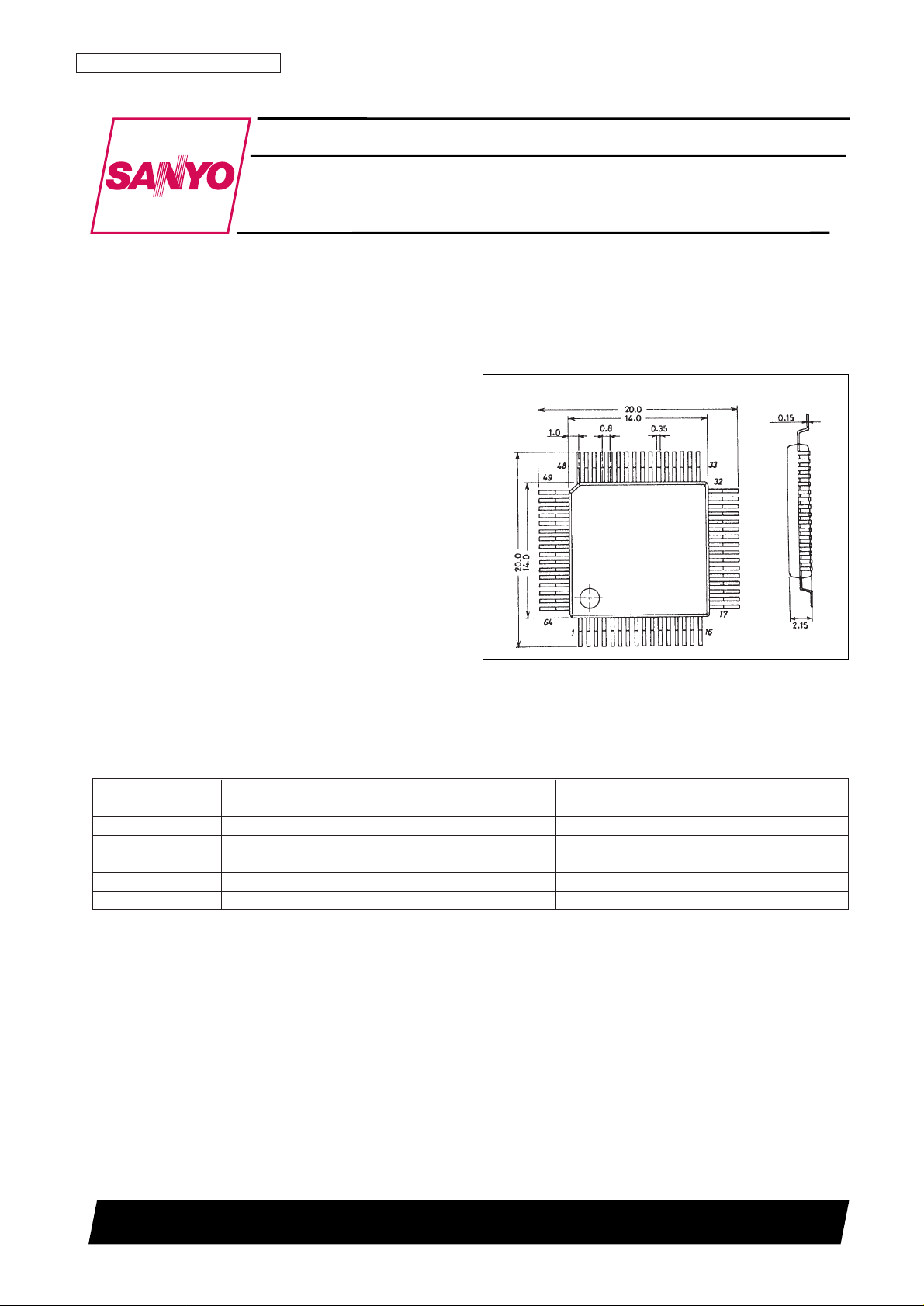
Package Dimensions
unit: mm
3057-QIP64A
SANYO: QIP64A
[LC5852N]
LC5852N
SANYO Electric Co.,Ltd. Semiconductor Bussiness Headquarters
TOKYO OFFICE Tokyo Bldg., 1-10, 1 Chome, Ueno, Taito-ku, TOKYO, 110-8534 JAPAN
Four-Bit Single-Chip Microcontroller with
On-Chip LCD Drivers for Small-Scale Control in
Medium-Speed Applications
CMOS LSI
Power supply option Cycle time Power supply voltage range Note
EXT-V 10 µs V
SS
2 = –4.0 to –5.5 V When using an 800 kHz ceramic resonator
EXT-V 20 µs V
SS
2 = –4.0 to –5.5 V When using a 400 kHz ceramic resonator
EXT-V 61 µs V
SS
2 = –2.3 to –5.5 V When using a 65 kHz crystal oscillator
EXT-V 122 µs, 244 µs V
SS
2 = –2.0 to –5.5 V When using a 32 kHz crystal oscillator
Li 122 µs, 244 µs V
SS
2 = –2.6 to –3.6 V* When using a 32 kHz crystal oscillator
Ag 122 µs, 244 µs V
SS
1 = –1.3 to –1.65 V When using a 32 kHz crystal oscillator
Note: * When the backup flag is set, the BAK pin is shorted to VSS2. (See the user’s manual for details.)
• Low current drain HALT mode (typical)
— Ceramic oscillator (CF): 400 kHz (5.0 V) 150 µA
— Crystal oscillator (Xtal): 32 kHz (1.5 V, Ag specifications) 2.0 µA (for LCD biases other than 1/3)
3.5 µA (for an LCD bias of 1/3)
— Crystal oscillator (Xtal): 32 kHz (3.0 V, Li specifications) 1.0 µA (for LCD biases other than 1/3)
5.0 µA (for an LCD bias of 1/3)
Page 2

• Timer functions
— One six-bit programmable timer
— Time base timer (for clock applications)
• Standby functions
— Clock standby function (HALT mode)
The LC5852N provides a halt function that reduces
power dissipation. In halt mode, only the oscillator,
divider and LCD driver circuits operate. All other
internal operations are stopped. This mode allows
the LC5852N to easily implement a low-power
clock function.
— Full standby function (HOLD mode)
— HALT mode is cleared by two external factors and
two internal factors.
• Improved I/O functions
— External interrupt pins
— Input pins that can clear HALT mode (up to 9 pins)
— Input ports with software controllable input resistors:
up to 8 pins
— Input ports with built-in floating prevention circuits:
up to 8 pins
— LCD drivers; common: 4 pins,
segment pins: 25 pins
— General-purpose I/O ports: 8 pins
— General-purpose inputs: 9 pins
— General-purpose outputs (1): 6 pins
(ALM pin, LIGHT pin)
— General-purpose outputs (2): 25 pins
(when all 25 LCD segment ports are used as generalpurpose outputs)
— Pseudo-serial output port: 1 set
(Three pins: output, BUSY, clock)
Function Overview
• Program ROM: 2048 × 15 bits
• On-chip RAM: 128 × 4 bits
• All instructions execute in a single cycle
• HALT mode clear and interrupt functions
(External factors)
Changes in the S and M port input signals
Changes in the INT pin input signal
(Internal factors)
Overflow from the clock divider circuit
Timer underflow
• Subroutines can be nested up to four levels (including
interrupts)
• Powerful hardware to improve processing capabilities
— On-chip segment PLA circuit and segment decoder:
The LCD driver outputs can handle LCD panel
segment display without incurring software
overhead.
— All LCD driver output pins can be switched to be
used as output ports.
— One six-bit programmable timer
— Part of the RAM area can be used as a working area.
— Built-in clock oscillator and 15-stage divider (also
used for LCD alternation signal generation)
• Highly flexible LCD panel drive output pins (25)
Supported Maximum number Required
drive types of segments common pins
1/3 bias—1/4 duty......100 segments ..........4 pins
1/3 bias—1/3 duty......75 segments ............3 pins
1/2 bias—1/4 duty......100 segments ..........4 pins
1/2 bias—1/3 duty......75 segments ............3 pins
1/2 bias—1/2 duty......50 segments ............2 pins
Static ..........................25 segments ............1 pin
— The LCD output pins can be converted to use as
general-purpose output pins.
CMOS type: 25 pins (maximum)
p-channel open drain type: 3 pins (maximum)
• An oscillator appropriate for the system specifications
can be selected.
32 or 65 kHz crystal oscillator, or
400 or 800 kHz ceramic oscillator
Delivery formats
QIP-64A or chip product
No. 4365-2/29
LC5852N
Page 3
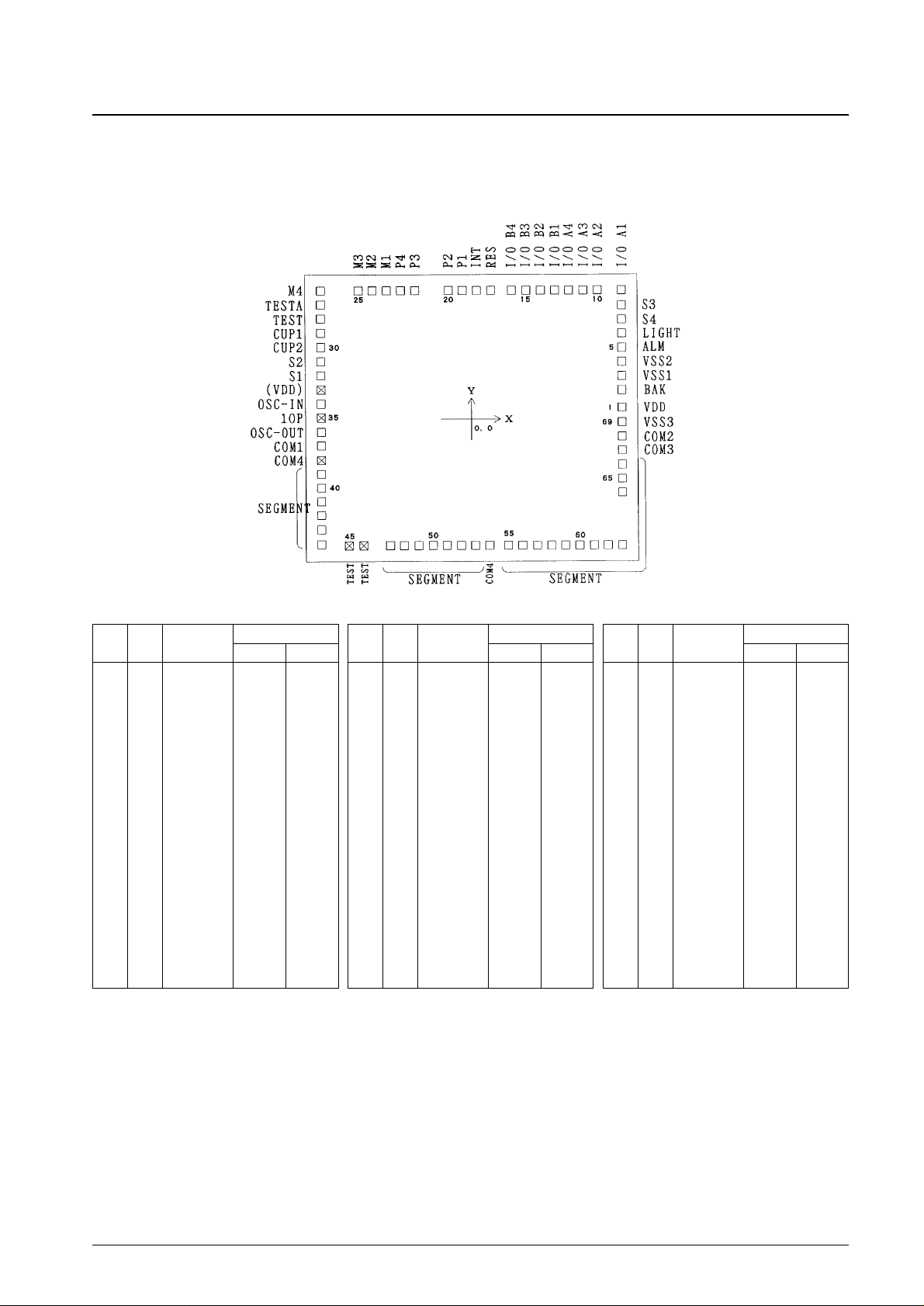
Pin and Pad Assignment
Chip size: 4.19 × 3.66 mm
Pad size: 120 × 120 µm
Chip thickness: 480 µm (chip specification products)
Note: 1. The pin numbers are those for the QIP-64A mass production package.
2. The pad coordinates given above take the center of the chip as the origin and specify the center of the pad.
3. TESTA pin (pin 2) in the QIP-64A product must be connected to the minus side of the power supply.
4. TEST pin (pin 3) in the QIP-64A product must be left open.
5. Pad 27 in the chip product must either be connected to the minus side of the power supply or left open.
6. Pads 28, 45 and 46 in the chip product must be left open.
7. If the chip product is used, the substrate must be connected to V
DD
.
8. Do not use dip-soldering techniques to mount the QIP-64A package product.
No. 4365-3/29
LC5852N
Pin Pad
Symbol
Coordinates
No. No.
Xµm Yµm
40 1 V
DD
1899 138
41 2 BAK 1899 358
42 3 V
SS
1 1899 538
43 4 V
SS
2 1899 718
44 5 ALM 1899 898
45 6 LIGHT 1899 1078
46 7 S4 1899 1258
47 8 S3 1899 1438
48 9 I/O A1 1899 1630
49 10 I/O A2 1595 1630
50 11 I/O A3 1415 1630
51 12 I/O A4 1235 1630
52 13 I/O B1 1055 1630
53 14 I/O B2 875 1630
54 15 I/O B3 695 1630
55 16 I/O B4 515 1630
56 17 RES 253 1630
57 18 INT 73 1630
58 19 P1 –107 1630
59 20 P2 –287 1630
60 21 P3 –707 1630
61 22 P4 –887 1630
62 23 M1 –1067 1630
Pin Pad
Symbol
Coordinates
No. No.
Xµm Yµm
63 24 M2 –1247 1630
64 25 M3 –1427 1630
1 26 M4 –1899 1630
2 27 TESTA –1899 1450
3 28 TEST –1899 1270
4 29 CUP1 –1899 1090
5 30 CUP2 –1899 910
6 31 S2 –1899 730
7 32 S1 –1899 550
— 33 (V
DD
) –1899 370
8 34 OSC-IN –1899 190
— 35 10P –1899 10
9 36 OSC-OUT –1899 –169
10 37 COM1 –1899 –349
— 38 COM4 –1899 –529
11 39 Seg01 –1899 –709
12 40 Seg02 –1899 –889
13 41 Seg03 –1899 –1069
14 42 Seg04 –1899 –1249
15 43 Seg05 –1899 –1429
16 44 Seg06 –1899 –1609
— 45 TEST –1553 –1630
— 46 TEST –1373 –1630
Pin Pad
Symbol
Coordinates
No. No.
Xµm Yµm
17 47 Seg07 –1033 –1630
18 48 Seg08 –853 –1630
19 49 Seg09 –673 –1630
20 50 Seg10 –493 –1630
21 51 Seg11 –313 –1630
22 52 Seg12 –133 –1630
23 53 Seg13 46 –1630
24 54 COM4 226 –1630
25 55 Seg14 459 –1630
26 56 Seg15 639 –1630
27 57 Seg16 819 –1630
28 58 Seg17 999 –1630
29 59 Seg18 1179 –1630
30 60 Seg19 1359 –1630
31 61 Seg20 1539 –1630
32 62 Seg21 1719 –1630
33 63 Seg22 1899 –1630
34 64 Seg23 1899 –954
35 65 Seg24 1899 –774
36 66 Seg25 1899 –594
37 67 COM3 1899 –414
38 68 COM2 1899 –234
39 69 V
SS
3 1899 –54
Page 4

System Block Diagram
LC5852N System Block Diagram
No. 4365-4/29
LC5852N
AC: Accumulator
ALU: Arithmetic and logic unit
INT CTL: Interrupt control circuit
PC: Program counter
TM: Preset timer (6 bits)
IR: Instruction register
HALT: Intermittent control circuit
SCG: System clock generator
STS1: Status register 1
STS2: Status register 2
STS3: Status register 3
CF: Carry flag
BCF: Backup flag
SCF1: M port flag
SCF2: STS3 flag
SCF3: S port flag
SCF4: INT signal change flag
SCF5: Timer overflow flag
ø15: Contents of the fifteenth stage of the divider
circuit
SCF7: Divider circuit overflow flag
Page 5
Pin Functions
No. 4365-5/29
LC5852N
Pin I/O
QIP-64
Function Option At reset
Pin No.
V
DD
BAK
V
SS
1
V
SS
2
V
SS
3
CUP1
CUP2
OSC-IN
OSC-OUT
10P
S1
S2
S3
S4
M1
M2
M3
M4
I/O A1
I/O A2
I/O A3
I/O A4
I/O B1
I/O B2
I/O B3
I/O B4
P1
P2
P3
P4
ALM
LIGHT
—
—
—
—
—
—
—
Input
Output
—
Input
Input
I/O
I/O
Output
Output
Output
40
41
42
43
39
4
5
8
9
—
7
6
47
46
62
63
64
1
48
49
50
51
52
53
54
55
58
59
60
61
44
45
Power supply plus side
LSI internal logic block minus power supply
In Li specification products, connect a capacitor between BAK and V
DD
to prevent incorrect operation.
Power supply minus side
• External component connections differ depending on mask options
and other factors.
In products for Ag use, connect V
SS
1 to the power supply minus side.
In other products, connect V
SS
2 to the power supply minus side.
• The pins other than the minus pin are used for the LCD driver power
supply.
Connections for the LCD drive voltage boost (cut) capacitor.
Used for real-time clock and the system clock.
Connected to OSC-IN or OSC-OUT and used for the oscillator phase
compensation capacitor. Can only be used in the chip product.
Dedicated input port
• Includes either a ø10 (32 ms), ø8 (8 ms), or ø2 (2 ms) chattering
exclusion circuit (PLA mask option).
* These values are for the case where a 32.768 kHz crystal is used.
• Pull-down resistors are built in.
Dedicated input port
• Input connections for acquiring data to internal RAM
• Pull-down resistors are built in.
I/O port
• Input connections for acquiring data to internal RAM
• Output connections for data output from internal RAM
• The input or output state can be switched by two instructions.
I/O port
• Input connections for acquiring data to internal RAM
• Output connections for data output from internal RAM
• The input or output state can be switched by two instructions.
Output port
• Output connections for data output from internal RAM
Dedicated output
This pin can output a signal modulated either at 4 kHz or 2 kHz, or at
4 kHz or 1 kHz under program control. Alternatively, an unmodulated
signal can be output.
* These values are for the case where a 32.768 kHz crystal is used.
Dedicated output
This pin can drive a power transistor.
• Ag specifications
• Li specifications
• EXT-V
specifications
• Crystal oscillator
use (XT option)
• Ceramic resonator
use (CF option)
The CF option can
only be specified for
EXT-V specification
products.
Inclusion
(or exclusion) of a
low level hold
transistor
Inclusion
(or exclusion) of a
low level hold
transistor
• Modulated signals
(4 kHz, 2 kHz, or
unmodulated)
• Modulated signals
(4 kHz, 1 kHz, or
unmodulated)
Backup flag set
Backup flag cleared
(depending on the
power supply option)
The pull-down
resistor transistor is
on.
The pull-down
resistor transistor is
on.
Input mode
Input mode
Either a high- or
low-level output.
(Undefined)
Low-level output
Low-level output
Continued on next page.
Page 6
Continued from preceding page.
No. 4365-6/29
LC5852N
Pin I/O
QIP-64
Function Option At reset
Pin No.
RES
INT
TESTA
TEST
Seg1
Seg2 to
Seg25
COM1
COM2
COM3
COM4
Input
Input
Input
—
Output
Output
56
57
2
3
11
12 to36
10
38
37
24
LSI internal reset input
• Reset can be performed on either a high or low input level.
• Built-in pull-up or pull-down resistor
Note: The applied signal must be held for at least 500 µs.
External interrupt request input
• Interrupt detection can be performed for either falling or rising edges.
• Built-in pull-up or pull-down resistor
Test input
• QIP-64 products: connect to the power supply – side
• Chip products: Leave open or connect to the power supply – side
Test input
This pin must be left open. (It cannot be used in user systems.)
• LCD drive/general-purpose output pins
— LCD drive
I STATIC
II 1/2 bias – 1/2 duty
III 1/2 bias – 1/3 duty
IV 1/2 bias – 1/4 duty
V 1/3 bias – 1/3 duty
VI 1/3 bias – 1/4 duty
Items I to V are specified as master options.
• General-purpose output mode (CMOS output)
— LCD/general-purpose output control under program control is
disabled by adoption of the segment PLA.
— Arbitrary combinations of LCD drive and general purpose outputs
are possible.
LCD common polarity drive outputs
These pins are used as follows depending on the LCD drive method
used.
(Note that these are typical specifications for 32.768 kHz when ø0 is
used for the alternation frequency.)
Note: An × indicates that the corrsponding common pin is not used
with that LCD drive method.
LCD drive type. Do not use hold mode in CF specification
products that use the LCD driver.
(The alternation frequency signal is stopped in hold mode.)
Pull-up or pull-down
resistor selection
• Pull-up or pulldown resistor
selection
• Signal change
type (rising or
falling) selection
• Switching between
LCD drive outputs
and generalpurpose outputs
• LCD drive method
switching
— STATIC
— 1/2 bias –
1/2 duty
— 1/2 bias –
1/3 duty
— 1/2 bias –
1/4 duty
— 1/3 bias –
1/3 duty
— 1/3 bias –
1/4 duty
• General-purpose
outputs
— CMOS
• LCD drive
— All segments
lit
— All segments
off
* Set by a mask
option
• General-purpose
outputs
— High level
— Low level
* Set by a mask
option
Static 1/2 duty 1/3 duty 1/4 duty
COM1
❍ ❍ ❍ ❍
COM2
× ❍ ❍ ❍
COM3
× × ❍ ❍
COM4
× × × ❍
Alternation
32 Hz 32 Hz 42.7 Hz 32 Hz
frequency
Page 7
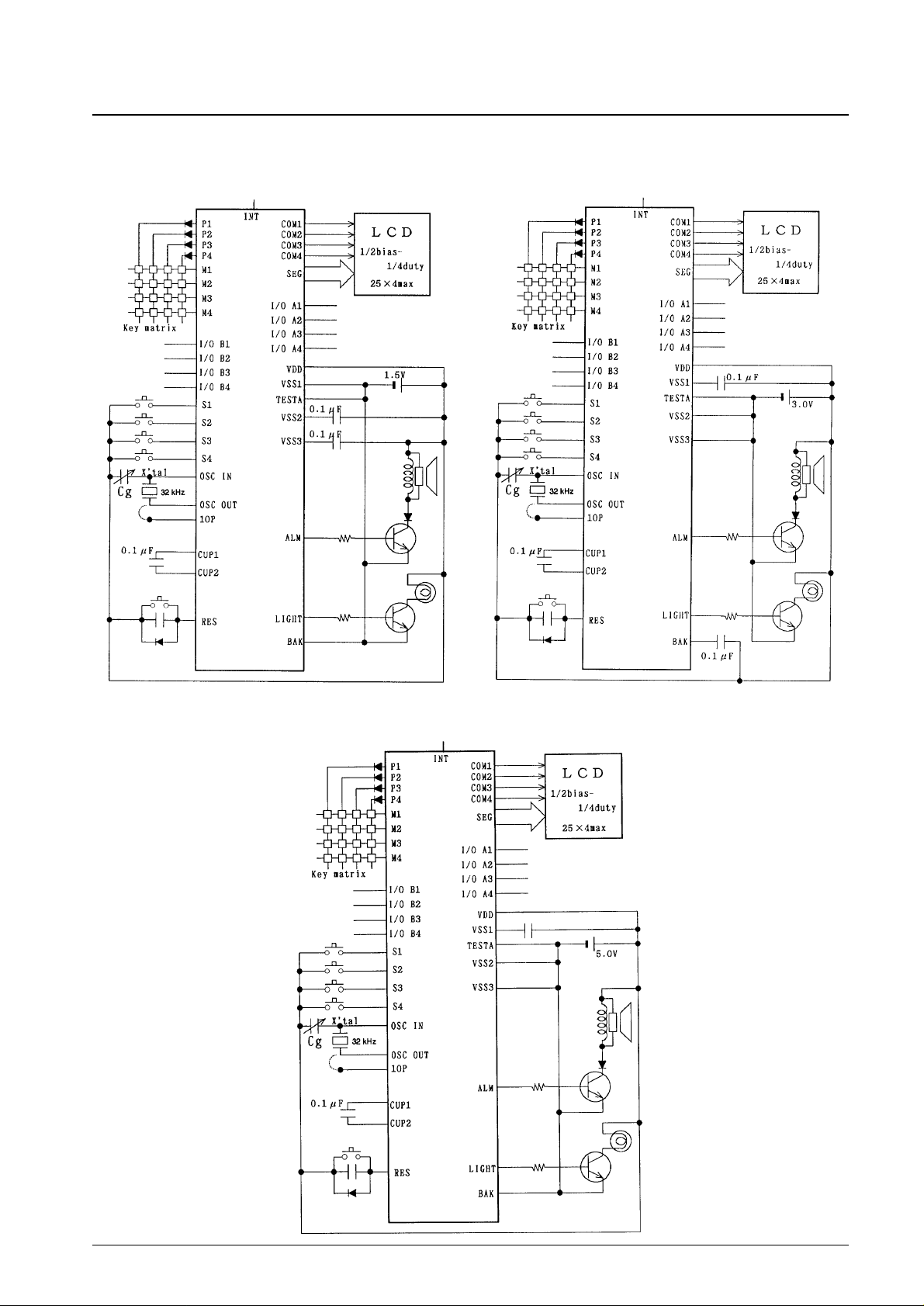
Application Circuit Examples
1. Representative application for Ag specification
products (1/3 bias - 1/4 duty)
3. Representative application for EXT-V specification
products (1/2 bias - 1/4 duty)
2. Representative application for lithium specification
products (1/2 bias - 1/4 duty)
No. 4365-7/29
LC5852N
Page 8

Oscillator Circuit Options
No. 4365-8/29
LC5852N
Option Circuit Form Note
CF
• 400 kHz
• 800 kHz
Xtal
(32.768 kHz)
Xtal
(65 kHz)
• The cycle time is 4 × n times the f1 period
(n : 2).
• The divider outputs (ø1 to ø15) are used,
for example, as the LCD drive waveform
generation clock and as the S and K port
chattering prevention clock.
• The cycle time is four times the f1 period.
• The divider outputs (ø1 to ø15) are used,
for example, as the LCD drive waveform
generation clock, as the S and K port
chattering prevention clock and as a clock
time base.
• The 10P connection can only be used in
chip products.
• The cycle time is four times the f1 period.
(Used when the cycle time is 61 µs.)
• The divider outputs (ø1 to ø15) are used,
for example, as the LCD drive waveform
generation clock and as the S and K port
chattering prevention clock.
• The 10P connection can only be used in
chip products.
Page 9
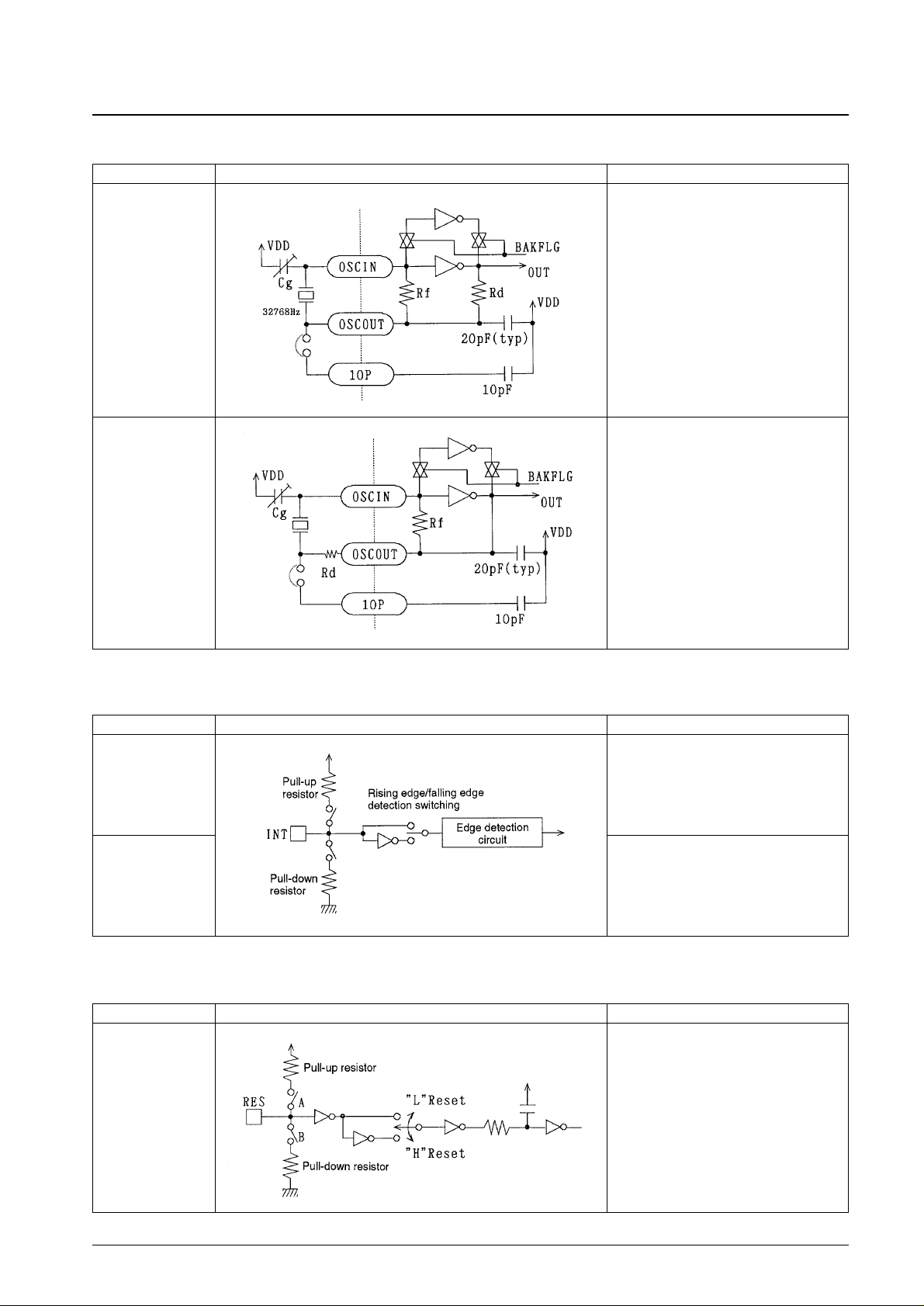
Crystal Oscillator Options
INT Pin Options
RES Pin Options
No. 4365-9/29
LC5852N
Option Circuit Form Note
32 kHz
65 kHz
The resistor Rd for use with a 32 kHz
frequency is built in.
Option Circuit Form Note
Pull-up resistor,
pull-down resistor, or
resistor open selection
Rising edge, falling
edge detection
selection
Built-in resistor selection
• Use of the pull-up resistor
• Use of the pull-down resistor
• Open
Signal change edge detection selection
• Rising edge detection
• Falling edge detection
Option Circuit Form Note
Pull-up resistor,
pull-down resistor, or
resistor open and
level selection
Built-in resistor and polarity selection
• Pull-up resistor and reset on low
• Pull-down resistor and reset on high
• Both resistors open and reset on low
• Both resistors open and reset on high
Page 10

Input Port Options
The use of the low level hold transistor can be specified individually for each pin in the S1 to S4 and M1 to M4 ports.
1. The S port includes independent (in bit units) chattering exclusion circuits with periods of ø10, ø8, or ø6.
2. The M port includes chattering exclusion circuits that operate for halt mode clear request signals.
These circuits exclude chattering for periods of ø10, ø8, or ø6 when three of the ports are at the low level and a
signal change occurs on the remaining port.
LCD Output Options
No. 4365-10/29
LC5852N
Option Circuit Form Note
Use of the hold
transistor
(low level hold
transistor)
Hold transistor unused
(open)
This option can be specified individually for
each pin in S1 to S4 and M1 to M4.
When use of the hold transistor is selected:
• This transistor is used to reduce the current
drain in the pull-up or pull-down resistor
when, for example, a push-button switch is
used for S1 or a slide switch is used for S2.
• When the input open specifications are
used, this transistor turns the resistor on
prior to reading the input value and then
turns the resistor off after the input value is
read. If the input is floating when read, the
low-level input hold transistor will operate
and hold that level.
When the hold transistor is unused:
• The pull-down transistor can be used as a
pull-down resistor.
• The pull-down transistor can be turned on
and off under program control.
• The pull-down resistor can be used in the
on state without change.
• Select the unused option if the input is
connected to an external control signal line
that will never go to the floating state.
• On reset
— The resistor will be in the on state during
the reset period.
— The resistor will keep up the on state
when reset is cleared.
Option Circuit Form
LCD drive
CMOS output port
P-channel open-drain
output port
• Used as LCD segment drive pins
• The LCD drive type is specified independently.
The LCD drive type is common to all LCD drive pins and can be selected from the following set:
static, 1/2 bias—1/2 duty, 1/2 bias—1/3 duty, 1/2 bias—1/4 duty, 1/3 bias—1/3 duty, or 1/3 bias—1/4 duty.
• General-purpose CMOS output ports
• General-purpose p-channel open-drain output ports
This option can be specified for three specific ports using PLA option specification.
Available ports...Pads 64 to 66 (pins 34 to 36)
Page 11

Mask Option Overview
1. Power supply specification selection
• Ag (Silver battery/1.5 V) specifications
• Li (Lithium battery/3.0 V) specifications
• EXT-V specifications (the operating voltage range depends on the oscillator used)
2. Oscillator selection
• Crystal oscillator (32.768 kHz)
• Crystal oscillator (65.536 kHz)
• Ceramic oscillator
3. LCD drive
• Static
• 1/2 bias—1/2 duty
• 1/2 bias—1/3 duty
• 1/2 bias—1/4 duty
• 1/3 bias—1/3 duty
• 1/3 bias—1/4 duty
Note: The LCD ports can all be used as general-purpose outputs. In this case, specify the “UNUSE” option.
6. LCD alternation frequency
• SLOW (OSC/2048)
• TYP (OSC/1024)
• FAST (OSC/512)
• STOP
5. S port low-level hold transistor
• Level hold transistor present
• No level hold transistor
6. M port low-level hold transistor
• Level hold transistor present
• No level hold transistor
7. S and M port chattering exclusion frequency
• SLOW (OSC/1024)
• TYP (OSC/256)
• FAST (OSC/64)
8. INT pin resistor selection and signal edge type selection
• Pull-up resistor (negative)
• Pull-down resistor (positive)
• Open (negative)
• Open (positive)
9. External reset
• RES pin
• Simultaneous input to S1 through S4
10. RES pin
• Pull-up resistor (low-level reset)
• Pull-down resistor (high-level reset)
• Open (low-level reset)
• Open (high-level reset)
11. Power-on reset function (internal reset)
• USE
• UNUSE
12. Timer input clock
• SLOW (OSC/512)
• FAST (OSC/8)
13. Alarm modulation base frequency
• SLOW (OSC/8, OSC/32)
• TYP (OSC/8, OSC/16)
14. Cycle time
• SLOW (OSC/8)
• FAST (OSC/4)
Note: Specify “SLOW” for this option if a ceramic oscillator is used.
No. 4365-11/29
LC5852N
Page 12

Internal Register Functions
No. 4365-12/29
LC5852N
Symbol R/W Function
Initialization
value at reset
PC
ROM
RAM
—
R/O
R/W
Program counter
The PC is an 11-bit counter that specifies the program memory (ROM) address of the next instruction to
be executed.
Normally, the PC is incremented on each instruction execution, from 000H to 7FFH. However, when a
branch or subroutine call is executed, or when an interrupt or initializing reset occurs, the PC is set to a
value corresponding to the particular operation. The table below shows how the PC is set for these
operations.
Page: ROM paging performed in 1024 word pages
Pages are specified with the SF and RF instructions.
P0 – P9: Instruction code bits (immediate data)
Program memory
The on-chip ROM consists of 2048 15-bit words and holds the user programs to be executed.
Data memory
The on-chip RAM consists of 128 4-bit digits of static RAM in two pages with 64 4-bit digits per page.
This RAM has the following features:
• RAM addresses can be specified directly (immediate addressing) as values in the range 00H to 3FH.
• Arithmetic operations can be performed between the AC and any RAM location.
• Due to the provision of the segment PLA circuit, RAM dedicated to display is not required.
• RAM locations 38H to 3FH have a function that allows direct arithmetic operations with other data
without using the AC.
• The AC is used for RAM input, i.e., writing.
Undefined
PC
PC10
PC9 PC8 PC7 PC6 PC5 PC4 PC3 PC2 PC1 PC0
Operation
Initializing reset 0 0 0 0 0 0 0 0 0 0 0
INT pin external interrupt
0 0 0 0 0 0 1 0 0 0 0
S or M port external
0 0 0 0 0 0 1 0 1 0 0
interrupt
Timer internal interrupt
0 0 0 0 0 0 1 1 0 0 0
Divider internal interrupt 0 0 0 0 0 0 1 1 1 0 0
Unconditional jump (JMP) Page P9 P8 P7 P6 P5 P4 P3 P2 P1 P0
Conditional jump
(BAB0, BAB1, BAB2, BAB3, Page P9 P8 P7 P6 P5 P4 P3 P2 P1 P0
BAZ, BANZ, BCH, BCNH)
Subroutine call instruction
Page P9 P8 P7 P6 P5 P4 P3 P2 P1 P0
(CALL)
Return instruction
CALL address + 1
(RTS, RTSR)
Continued on next page.
Page 13

Continued from preceding page.
No. 4365-13/29
LC5852N
Symbol R/W Function
Initialization
value at reset
RAM
AC
STACK
APG
OPG
TIM
R/W
R/W
R/W
R/W
R/W
W
Accumulator
Stack pointer
The stack consists of four 13-bit words supporting subroutine calls and interrupts up to four levels deep.
P0 to P10: Program counter (PC)
APG: RAM page flag
OPG: ROM page flag
RAM page flag
The RAM page flag is a single bit that allows the RAM to be expanded to two pages, where a single RAM
page is 64 × 4 bits.
ROM page flag
The ROM page flag is a single bit that allows the ROM to be expanded to two pages, where a single ROM
page is 1024 × 15 bits.
Timer counter
The timer is a 6-bit down counter.
The timer is set from immediate data in an instruction.
Undefined
Undefined
01H
00H
00H
Undefined
Continued on next page.
Page 14

Continued from preceding page.
No. 4365-14/29
LC5852N
Symbol R/W Function
Initialization
value at reset
STS1
STS2
STS3
R/W
R/O
R/O
Status register 1 (STS1)
Status register 1 is a four-bit register whose bits are used as shown below.
* The test flags cannot be used by application programs.
Status register 2 (STS2)
Status register 2 is a four-bit register whose bits are used as shown below.
SCF1: Set when there was a change in an M port signal (when enabled by an SSW instruction).
SCF2: Set when any bit in STS3 is set.
SCF3: Set when there was a change in an S port signal (when enabled with an SSW instruction).
Status register 3 (STS3)
Status register 3 is a four-bit register whose bits are used as shown below.
SCF4: Set when there was a change in the INT pin signal (when enabled by an SIC instruction).
SCF5: Timer underflow (when enabled by an SIC instruction)
SCF4: Divider overflow (when enabled by an SIC instruction)
00H
Undefined
Undefined
Page 15

Specifications
These electrical specifications are provisional and subject to change.
EXT-V Specifications
Absolute Maximum Ratings at VDD= 0 V
Allowable Operating Ranges at Ta = –20 to +70°C, VDD= 0 V
No. 4365-15/29
LC5852N
Parameter Symbol Conditions/Pins min typ max Unit
V
SS
1 –7.0 +0.3 V
Maximum supply voltage
V
SS
2 –7.0 +0.3 V
V
SS
3 LCD drive method (1/3 bias) –8.5 +0.3 V
V
SS
3 LCD drive method (Any method other than 1/3 bias) –7.0 +0.3 V
S1 to 4, M1 to 4, I/OA1 to 4, I/OB1 to 4, INT, RES,
Maximum input voltage VIN1 OSCIN, 10P, TESTA (with I/OA1 to 4 and I/OB1 to 4 VSS2 – 0.3 +0.3 V
in input mode, 10P is for chip products)
ALM, LIGHT, P1 to 4, CUP2, OSCOUT, TEST,
V
OUT
1 I/OA1 to 4, I/OB1 to 4 VSS2 – 0.3 +0.3 V
Maximum output voltage
(with I/OA and I/OB in output mode)
V
OUT
2 SEGOUT, COM1 to 4, CUP1 VSS3 V
Operating temperature Topr –20 +70 °C
Storage temperature Tstg –30 +125 °C
Parameter Symbol Conditions/Pins min typ max Unit
V
SS
1 –5.5 –1.3 V
Supply voltage V
SS
2 32 kHz crystal oscillator specifications –5.5 –2.0 V
V
SS
3 –8.25 –2.0 V
V
SS
1 –5.5 –1.3 V
Supply voltage V
SS
2 65 kHz crystal oscillator specifications –5.5 –2.3 V
V
SS
3 –8.25 –2.3 V
V
SS
1 –5.5 –1.7 V
Supply voltage V
SS
2 External input used –5.5 –3.5 V
V
SS
3 –8.25 –3.5 V
V
SS
1 –5.5 –2.0 V
Supply voltage V
SS
2 400 kHz CF specifications –5.5 –4.0 V
V
SS
3 –8.25 –4.0 V
Input high level voltage V
IH
1
All input ports except OSCIN
0.3 × VSS2 0 V
Input low level voltage V
IL
1 VSS2 0.7 × VSS2 V
Input high level voltage V
IH
2
OSCIN pin, when external input used, Figure 8
0.2 × VSS2 0 V
Input low level voltage V
IL
2 VSS2 0.8 × VSS2 V
OSCIN/OSCOUT,
Operating frequency fopg1 VSS2 = –2.0 to –5.5 V 32 kHz crystal oscillator, 32 33 kHz
Figure 2
OSCIN/OSCOUT,
Operating frequency fopg2 V
SS
2 = –2.3 to –5.5 V 65 kHz crystal oscillator, 60 66 kHz
Figure 2
Operating frequency fopg3 V
SS
2 = –3.5 to –5.5 V
OSCIN external input,
32 220 kHz
Figure 8
Operating frequency fopg4 V
SS
2 = –4.0 to –5.5 V
OSCIN/OSCOUT,
360 400 440 kHz
CF 400 kHz, Figure 1
Operating frequency fopg5 VSS2 = –4.0 to –5.5 V
OSCIN/OSCOUT,
720 800 880 kHz
CF 800 kHz, Figure 1
Continued on next page.
Page 16

Electrical Characteristics at Ta = –20 to +70°C, VDD= 0 V
Note: * S1, S2, S3, S4, M1, M2, M3, M4
Parameter Symbol Conditions/Pins min typ max Unit
R
IN
1A
V
SS
2 = –2.9 V, Low-level hold transistor*,
10 200 kΩ
V
IN
= 0.8 × VSS2 Figure 3
Input resistance
R
IN
1B
V
SS
2 = –2.9 V, Low-level pull-in transistor*,
200 700 2000 kΩ
V
IN
= V
DD
Figure 3
R
IN
2A
V
SS
2 = –2.9 V,
INT pin pull-up resistor 200 700 2000 kΩ
V
IN
= VSS2
R
IN
2B
V
SS
2 = –2.9 V,
INT pin pull-down resistor 200 700 2000 kΩ
Input resistance
V
IN
= V
DD
RIN3
V
SS
2 = –2.9 V,
RES 5 50 kΩ
V
IN
= VDDor VSS2
Output high level voltage V
OH
(1)
V
SS
2 = –2.4 V,
ALM –1 –0.3 V
I
OH
= 1 mA
Output low level voltage V
OL
(1)
V
SS
2 = –2.4 V,
ALM V
SS
2 + 0.3 VSS2 + 1 V
I
OL
= 1 mA
Output high level voltage V
OH
(2)
V
SS
2 = –2.4 V,
LIGHT, Port P –1 –0.3 V
I
OH
= 0.3 mA
Output low level voltage V
OL
(2)
V
SS
2 = –2.4 V,
LIGHT, Port P V
SS
2 + 0.3 VSS2 + 1 V
I
OL
= 0.5 mA
Output high level voltage V
OH
(3)
V
SS
2 = –2.4 V,
I/O ports –1 –0.3 V
I
OH
= 0.1 mA
Output high level voltage V
OH
(4)
V
SS
2 = –2.4 V,
I/O ports –0.6 –0.2 V
I
OH
= –50 µA
Output low level voltage V
OL
(4)
V
SS
2 = –2.4 V,
I/O ports V
SS
2 + 0.3 VSS2 + 1 V
I
OL
= 0.1 mA
Segment driver output impedances
• When used as CMOS output ports
Output high level voltage V
OH
(5)
V
SS
2 = –2.4 V,
–1 –0.3 V
I
OH
= –10 µA
Output low level voltage V
OL
(5)
V
SS
2 = –2.4 V,
V
SS
2 + 0.3 VSS2 + 1 V
I
OL
= 100 µA
Output high level voltage V
OH
(6)
V
SS
2 = –2.4 V,
–1 –0.3 V
I
OH
= –5 µA
Output low level voltage V
OL
(6)
V
SS
2 = –2.4 V,
V
SS
2 + 0.3 VSS2 + 1 V
I
OL
= 20 µA
• When used as p-channel open-drain output ports
Output high level voltage V
OH
(5)
V
SS
2 = –2.4 V,
–1 –0.3 V
I
OH
= –10 µA
Output off leakage current I
OFF
VSS2 = –2.9 V,
1 µA
V
OL
= VSS2
• Static drive
Output high level voltage V
OH
(5)
V
SS
2 = –2.4 V,
–0.2 V
I
OH
= –0.4 µA,
All segments
Output low level voltage V
OL
(5)
V
SS
2 = –2.4 V,
V
SS
2 + 0.2 V
I
OL
= 0.4 µA
Output high level voltage V
OH
(7)
V
SS
2 = –2.4 V,
–0.2 V
I
OH
= –4 µA
COM1
Output low level voltage V
OL
(7)
V
SS
2 = –2.4 V,
V
SS
2 + 0.2 V
I
OL
= 4 µA
• Duplex drive (1/2 bias—1/2 duty)
Output high level voltage V
OH
(5)
V
SS
2 = –2.4 V,
–0.2 V
I
OH
= –0.4 µA
All segments
Output low level voltage V
OL
(5)
V
SS
2 = –2.4 V,
V
SS
2 + 0.2 V
I
OL
= 0.4 µA
Output high level voltage V
OH
(7)
V
SS
2 = –2.4 V,
–0.2 V
I
OH
= –4 µA
V
SS
2 = –2.4 V,
V
SS
2/2 VSS2/2
Output middle level voltage V
OMIOH
= –4µA, COM1, 2
– 0.2 + 0.2
V
I
OL
= 4 µA
Output low level voltage V
OL
(7)
V
SS
2 = –2.4 V,
V
SS
2 + 0.2 V
I
OL
= 4 µA
No. 4365-16/29
LC5852N
Segment
Pads 62 to 64,
QIP64 pins 34 to 36
Segment
Pads 62 to 64,
QIP64 pins 34 to 36
Segment
Pads 38 to 41 and 44 to 61,
QIP64 pins 11 to 23
and 25 to 33
Continued on next page.
Page 17

Continued from preceding page.
Electrical Characteristics at Ta = –20 to +70°C, VDD= 0 V
Note: * S1, S2, S3, S4, M1, M2, M3, M4
No. 4365-17/29
LC5852N
Parameter Symbol Conditions min typ max Unit
• 1/2 bias—1/3 duty and 1/2 bias—1/4 duty methods
Output high level voltage V
OH
(5)
V
SS
2 = –2.4 V,
–0.2 V
I
OH
= –0.4 µA
All segments
Output low level voltage V
OL
(5)
V
SS
2 = –2.4 V,
V
SS
2 + 0.2 V
I
OL
= 0.4 µA
Output high level voltage V
OH
(7)
V
SS
2 = –2.4 V,
–0.2 V
I
OH
= –4 µA
V
SS
2 = –2.4 V,
V
SS
2/2 VSS2/2
Output middle level voltage V
OMIOH
= –4 µA,
– 0.2 + 0.2
V
I
OL
= 4 µA
Output low level voltage V
OL
(7)
V
SS
2 = –2.4 V,
V
SS
2 + 0.2 V
I
OL
= 4 µA
• 1/3 bias—1/3 duty and 1/3 bias—1/4 duty methods
Output high level voltage V
OH
(5)
V
SS
2 = –2.4 V,
–0.2 V
I
OH
= –0.4 µA
V
OM
1-1
V
SS
2 = –2.4 V, VSS2/2 VSS2/2
V
Output middle level voltage
I
OH
= –0.4 µA
All segments
– 0.2 + 0.2
V
OM
1-2 IOL= 0.4 µA VSS2 – 0.2 VSS2 + 0.2 V
Output low level voltage V
OL
(5)
V
SS
2 = –2.4 V,
V
SS
3 + 0.2 V
I
OL
= 0.4 µA
Output high level voltage V
OH
(7)
V
SS
2 = –2.4 V,
–0.2 V
I
OH
= –4 µA
V
OM
2-1
V
SS
2 = –2.4 V, VSS2/2 VSS2/2
V
Output middle level voltage
I
OH
= –4 µA –0.2 +0.2
V
OM
2-2 IOL= 4 µA VSS2 – 0.2 VSS2 + 0.2 V
Output low level voltage V
OL
(7)
V
SS
2 = –2.4 V,
V
SS
3 + 0.2 V
I
OL
= 4 µA
COM1 to 3
(for 1/3 duty methods)
COM1 to 4
(for 1/4 duty methods)
COM1 to 3
(for 1/3 duty methods)
COM1 to 4
(for 1/4 duty methods)
Parameter Symbol Conditions min typ max Unit
R
IN
1A
V
SS
2 = –5.0 V, Low-level hold transistor*,
10 45 150 kΩ
V
IN
= 0.8 · VSS2 Figure 3
R
IN
1B
V
SS
2 = –5.0 V, Low-level pull-in transistor*,
100 350 1000 kΩ
V
IN
= V
DD
Figure 3
Input resistance R
IN
2A
V
SS
2 = –5.0 V,
INT pin pull-up resistor 100 350 1000 kΩ
V
IN
= VSS2
R
IN
2B
V
SS
2 = –5.0 V,
INT pin pull-down resistor 100 350 1000 kΩ
V
IN
= V
DD
RIN3
V
SS
2 = –5.0 V,
RES 10 20 50 kΩ
V
IN
= VDDor VSS2
Output high level voltage V
OH
(1)
V
SS
2 = –3.5 to –5.25 V,
ALM –1 –0.3 V
I
OH
= –1.5 mA
Output low level voltage V
OL
(1)
V
SS
2 = –3.5 to –5.25 V,
ALM V
SS
2 + 0.3 VSS2 + 1 V
I
OL
= 1.5 mA
Output high level voltage V
OH
(2)
V
SS
2 = –3.5 to –5.25 V,
LIGHT, Port P –1 –0.3 V
I
OH
= –0.5 mA
Output low level voltage V
OL
(2)
V
SS
2 = –3.5 to –5.25 V,
LIGHT, Port P V
SS
2 + 0.3 VSS2 + 1 V
I
OL
= 0.7 mA
Output high level voltage V
OH
(3)
V
SS
2 = –3.5 to –5.25 V,
I/O ports –1 –0.3 V
I
OH
= –0.13 mA
Output high level voltage V
OH
(4)
V
SS
2 = –3.5 to –5.25 V,
I/O ports –0.6 –0.2 V
I
OH
= –50 µA
Output low level voltage V
OL
(4)
V
SS
2 = –3.5 to –5.25 V,
I/O ports V
SS
2 + 0.3 VSS2 + 1 V
I
OL
= 0.13 mA
Continued on next page.
Page 18

Continued from preceding page.
No. 4365-18/29
LC5852N
Parameter Symbol Conditions min typ max Unit
Segment driver output impedances
• When used as CMOS output ports
Output high level voltage V
OH
(5)
V
SS
2 = –3.5 to –5.25 V,
–1 –0.3 V
I
OH
= –15 µA
Output low level voltage V
OL
(5)
V
SS
2 = –3.5 to –5.25 V,
V
SS
2 + 0.3 VSS2 + 1 V
I
OL
= 150 µA
Output high level voltage V
OH
(6)
V
SS
2 = –3.5 to –5.25 V,
–1 –0.3 V
I
OH
= –10 µA
Output low level voltage V
OL
(6)
V
SS
2 = –3.5 to –5.25 V,
V
SS
2 + 0.3 VSS2 + 1 V
I
OL
= 60 µA
• When used as p-channel open-drain output ports
Output high level voltage V
OH
(5)
V
SS
2 = –3.5 to –5.25 V,
–1 –0.3 V
I
OH
= –15 µA
Output off leakage current I
OFF
VSS2 = –3.5 to –5.25 V,
1 µA
V
OL
= VSS2
• Static drive
Output high level voltage V
OH
(5)
V
SS
2 = –3.5 to –5.25 V,
–0.2 V
I
OH
= –0.4 µA
All segments
Output low level voltage V
OL
(5)
V
SS
2 = –3.5 to –5.25 V,
V
SS
2 + 0.2 V
I
OL
= 0.4 µA
Output high level voltage V
OH
(7)
V
SS
2 = –3.5 to –5.25 V,
–0.2 V
I
OH
= –4 µA
COM1
Output low level voltage V
OL
(7)
V
SS
2 = – 3.5 to –5.25 V,
V
SS
2 + 0.2 V
I
OL
= 4 µA
• Duplex drive (1/2 bias—1/2 duty)
Output high level voltage V
OH
(5)
V
SS
2 = –3.5 to –5.25 V,
–0.2 V
I
OH
= –0.4 µA
All segments
Output low level voltage V
OL
(5)
V
SS
2 = –3.5 to –5.25 V,
V
SS
2 + 0.2 V
I
OL
= 0.4 µA
Output high level voltage V
OH
(7)
V
SS
2 = –3.5 to –5.25 V,
–0.2 V
I
OH
= –4 µA
Output middle level voltage V
OM
2-1
V
SS
2 = –3.5 to –5.25 V,
COM1, 2
VSS2/2 VSS2/2
V
I
OH
= –4 µA, IOL= 4 µA – 0.2 +0.2
Output low level voltage V
OL
(7)
V
SS2 = –3.5 to –5.25 V,
V
SS
2 +0.2 V
I
OL
= 4 µA
• 1/2 bias—1/3 duty and 1/2 bias—1/4 duty methods
Output high level voltage V
OH
(5)
V
SS
2 = –3.5 to –5.25 V,
–0.2 V
I
OH
= –0.4 µA
All segments
Output low level voltage V
OL
(5)
V
SS
2 = –3.5 to –5.25 V,
V
SS
2 + 0.2 V
I
OL
= 0.4 µA
Output high level voltage V
OH
(7)
V
SS
2 = –3.5 to –5.25 V,
–0.2 V
I
OH
= –4 µA
Output middle level voltage V
OM
2-1
V
SS
2 = –3.5 to –5.25 V, VSS2/2 VSS2/2
V
I
OH
= –4 µA, IOL= 4 µA – 0.2 +0.2
Output low level voltage V
OL
(7)
V
SS
2 = –3.5 to –5.25 V,
V
SS
2 + 0.2 V
I
OL
= 4 µA
• 1/3 bias—1/3 duty and 1/3 bias—1/4 duty methods
Output high level voltage V
OH
(5)
V
SS
2 = –3.5 to –5.25 V,
–0.2 V
I
OH
= –0.4 µA
V
OM
1-1
VSS2 = –3.5 to –5.25 V,
V
SS
2/2 VSS2/2
V
Output middle level voltage
IOH= –0.4 µA,
All segments
– 0.2 +0.2
V
OM
1-2
I
OL
= 0.4 µA
V
SS
2 – 0.2 VSS2 + 0.2 V
Output low level voltage V
OL
(5)
V
SS
2 = –3.5 to –5.25 V,
V
SS
3 + 0.2 V
I
OL
= 0.4 µA
Output high level voltage V
OH
(7)
V
SS
2 = –3.5 to –5.25 V,
–0.2 V
I
OH
= –0.4 µA
V
OM
2-1
V
SS
2 = –3.5 to –5.25 V,
V
SS
2/2 VSS2/2
V
Output low level voltage
I
OH
= –4 µA, IOL= 4 µA
– 0.2 +0.2
V
OM
2-2 VSS2 – 0.2 VSS2 + 0.2 V
Output low level voltage V
OL
(7)
V
SS
2 = –3.5 to –5.25 V,
V
SS
3 + 0.2 V
I
OL
= 4 µA
Segment
Pads 62 to 64,
QIP64 pins 34 to 36
Segment
Pads 62 to 64,
QIP64 pins 34 to 36
COM1 to 3
(for 1/3 duty methods)
COM1 to 4
(for 1/4 duty methods)
COM1 to 3
(for 1/3 duty methods)
COM1 to 4
(for 1/4 duty methods)
Segment
Pads 38 to 41 and 44 to 61,
QIP64 pins 11 to 23
and 25 to 33
Continued on next page.
Page 19

Continued from preceding page.
No. 4365-19/29
LC5852N
Parameter Symbol Conditions min typ max Unit
Power supply leakage current I
LEK
VSS2 = VSS3 = –4.5 V Ta = 25°C 10 µA
Input leakage current I
IN
VSS2 = –2.0 to +4.5 V VIN= VSS2 to V
DD
–1 +1 µA
VSS1 VSS2 = –2.9 V
C1 = C2 = C3 = 0.1 µF,
–1.45 –1.35 V
Output voltage
V
SS
3 VSS2 = –2.9 V
fopg = 32.768 kHz,
Ta = 25°C, Figure 7
–4.35 –4.1 V
V
SS
1 VSS2 = –4.5 V
C1 = C2 = C3 = 0.1 µF,
–2.25 –2.2 V
Output voltage
V
SS
3 VSS2 = –4.5 V
fopg = 32.768 kHz,
Ta = 25°C, Figure 7
–6.70 –6.6 V
| I
DD
1 |
V
SS
2 = –2.9 V,
3.0 6.0 µA
Ta = 25°C, HALT mode
V
SS
2 = –4.5 V,
C1 = C2 = 0.1 µF, Cl = 25 kΩ,
Power supply current
Ta = 25°C, HALT mode,
fopg = 32.768 kHz,
| I
DD
2 |
Stack: Figure 9,
Cg = 20 pF
7 13 µA
1/3 bias—1/3 duty:
Figure 7,
other methods: Figure 4
V
SS
2 = –4.5 V,
Ta = 25°C, HALT mode
C1 = C2 = 0.1 µF, Cl = 25 kΩ,
Power supply current | I
DD
3 |
Stack: Figure 9,
fopg = 65.536 kHz, 10 20 µA
1/3 bias—1/3 duty:
Cg = 10 pF
Figure 7,
other methods: Figure 4
C1 = C2 = 0.1 µF,
Power supply current | I
DD
4 |
V
SS
2 = –4.5 V, fopg = 400 kHz,
90 150 µA
Ta = 25°C, HALT mode Cg = Cd = 100 pF or 330 pF,
Rf = 1 MΩ, Figure 6
C1 = C2 = 0.1 µF,
Power supply current | I
DD
5 |
V
SS
2 = –4.5 V, fopg = 800 kHz,
130 200 µA
Ta = 25°C, HALT mode Cg = Cd = 100 pF,
Rf = 1 MΩ, Figure 6
Ta = 25°C,
C1 = C2 = 0.1 µF,
Stack: Figure 9,
Cl = 25 kΩ,
Oscillator hold voltage | V
HOLD
1 | 1/3 bias—1/3 duty:
fopg = 32.768 kHz,
2.0 5.5 V
Figure 7,
Cg = 20 pF
other methods: Figure 4
C1 = C2 = 0.1 µF,
Oscillator hold voltage | V
HOLD
2 | Ta = 25°C
Cl = 25 kΩ,
2.3 5.5 V
fopg = 65.536 kHz,
Cg = 10 pF
Stack: Figure 10,
C1 = C2 = 0.1 µF,
1/3 bias—1/3 duty:
Cl = 25 kΩ, Figure 5,
Oscillator start voltage | VStt1 | Figure 7,
fopg = 32.768 kHz,
2.2 V
other methods: Figure 4,
Cg = 20 pF
Ta = 25°C
C1 = C2 = 0.1 µF, Cl = 25 kΩ,
Oscillator start voltage | VStt2 | Ta = 25°C Figure 5, fopg = 65.536 kHz, 2.6 V
Cg = 10 pF
V
SS
2 = –2.9 V,
C1 = C2 = 0.1 µF, Cl = 25 kΩ, 10 S
Oscillator start time TStt1
Ta = 25°C,
Figure 5, fopg = 32.768 kHz,
V
SS
2 = –4.5 V,
Cg = 20 pF 10 S
Ta = 25°C
V
SS
2 = –2.9 V,
C1 = C2 = 0.1 µF, Cl = 25 kΩ, 10 S
Oscillator start time TStt2
Ta = 25°C,
Figure 5, fopg = 65.536 kHz,
V
SS
2 = –4.5 V,
Cg = 10 pF 10 S
Ta = 25°C
fopg = 400 kHz, Figure 6,
Oscillator start voltage | VStt4 | Ta = 25°C Cg = Cd = 100 pF or 330 pF, 4.0 V
Rf = 1 MΩ
fopg = 400 kHz, Figure 6,
Oscillator hold voltage | V
HOLD
4 | Ta = 25°C Cg = Cd = 100 pF or 330 pF, 3.5 5.5 V
Rf = 1 MΩ
V
SS
2 = –4.5 V,
fopg = 400 kHz, Figure 6,
Oscillator start time TStt4
Ta = 25°C
Cg = Cd = 100 pF or 330 pF, 30 ms
Rf = 1 MΩ
Continued on next page.
Page 20

Continued from preceding page.
No. 4365-20/29
LC5852N
Parameter Symbol Conditions min typ max Unit
fopg = 800 kHz, Figure 6,
Oscillator start voltage | VStt5 | Ta = 25°C Cg = Cd = 100 pF, 4.0 V
Rf = 1 MΩ
fopg = 800 kHz, Figure 6,
Oscillator hold voltage | V
HOLD
5 | Ta = 25°C Cg = Cd = 100 pF, 3.5 5.5 V
Rf = 1 MΩ
V
SS
2 = –4.5 V,
fopg = 800 kHz, Figure 6,
Oscillator start time TStt5
Ta = 25°C
Cg = Cd = 100 pF, 30 ms
Rf = 1 MΩ
10P V
SS
2 = –2.9 V 10P pin (chip products only) 10 pF
Oscillator correction capacitance
10P V
SS
2 = –4.5 V 10P pin (chip products only) 10 pF
20P V
SS
2 = –2.9 V OSCOUT pin 20 pF
20P V
SS
2 = –4.5 V OSCOUT pin 20 pF
Figure 1 Ceramic Oscillator Specifications
Figure 3 S1 to S4 and M1 to M4 Input Circuits
Figure 5 Oscillator Start Voltage,
Oscillator Start Time and
Frequency Stability Test Circuit
Figure 2 Crystal Oscillator Specifications
(32 kHz or 65 kHz)
Figure 4 Power Supply Current and
Oscillator Hold Voltage Test Circuit
Figure 6 Oscillator Start Voltage,
Oscillator Start Time, Power Supply Current and
Oscillator Hold Voltage Test Circuit
Recommended Ceramic Oscillators
Manufacturer Murata Kyocera
Item frequency Type number Cg (pF) Cd (pF) Rf (MΩ) Type number Cg (pF) Cd (pF) Rf (MΩ)
400 kHz CSB400P 100 100 1 KBR-400B 330 330 1
800 kHz CSB800J 100 100 1 KBR-800H 100 100 1
Page 21

No. 4365-21/29
LC5852N
Figure 7 Power Supply Current and
Oscillator Hold Voltage Test Circuit
Figure 9 Power Supply Current and
Oscillator Hold Time Test Circuit
Figure 8 External Input Specifications
Page 22

These electrical specifications are provisional and subject to change.
Ag Specifications
Absolute Maximum Ratings at Ta = 25°C, VDD= 0 V
Allowable Operating Ranges at Ta = 25 ± 2°C, VDD= 0 V
Electrical Characteristics at Ta = 25 ± 2°C, VDD= 0 V
Note: * S1, S2, S3, S4, M1, M2, M3, M4
No. 4365-22/29
LC5852N
Parameter Symbol Conditions/Pins min typ max Unit
V
SS
1 –4.0 +0.3 V
Maximum supply voltage
V
SS
2 –4.0 +0.3 V
V
SS
3 LCD drive method (1/3 bias) –5.5 +0.3 V
V
SS
3 LCD drive method (methods other than 1/3 bias) –4.0 +0.3 V
S1 to 4, M1 to 4, I/OA1 to 4, I/OB1 to 4, INT, TESTA
Maximum input voltage VIN1 (with I/OA1 to 4 and I/OB1 to 4 in input mode), VSS1 – 0.3 +0.3 V
1OP, OSCIN, RES, BAK
ALM, LIGHT, P1 to 4, I/OA1 to 4, I/OB1 to 4,
V
OUT
1 CUP2 (with I/OA1 to 4 and I/OB1 to 4 in output mode), VSS1 – 0.3 +0.3 V
Maximum output voltage
TESTA, OSCOUT
V
OUT
3 SEGOUT, COM1 to 4, CUP1 VSS1 – 0.3 +0.3 V
Operating temperature Topr –20 +65 °C
Storage temperature Tstg –30 +125 °C
Parameter Symbol Conditions/Pins min typ max Unit
V
SS
1 V
BAK
= VSS1 –1.65 –1.3 V
Supply voltage
V
SS
2 –3.3 –2.4 V
V
SS
3 LCD drive method (1/3 bias) –4.95 –3.7 V
V
SS
3 LCD drive method (methods other than 1/3 bias) VSS3 = VSS2
Input high level voltage V
IH
S1 to 4, M1 to 4, I/OA1 to 4, I/OB1 to 4, RES, INT
–0.2 0 V
(with I/OA1 to 4 and I/OB1 to 4 in input mode)
Input low level voltage V
IL
S1 to 4, M1 to 4, I/OA1 to 4, I/OB1 to 4, INT
V
SS
1 VSS1 + 0.2 V
(with I/OA1 to 4 and I/OB1 to 4 in input mode)
Operating frequency fopg Ta = –20 to +65°C 32 33 kHz
Parameter Symbol Conditions/Pins min typ max Unit
R
IN
1A
V
SS
1 = –1.55 V, Low-level hold transistor*,
10 50 200 kΩ
V
IL
= VSS1 + 0.2 V Figure 1
R
IN
1B VSS1 = –1.55 V
Low-level pull-down resistor*,
200 550 2000 kΩ
Figure 1
Input resistance RIN2A
VSS1 = –1.55 V,
INT pull-up resistor 200 400 2000 kΩ
V
IL
= VSS1
R
IN
2B
V
SS
1 = –1.55 V,
INT pull-down resistor 200 550 2000 kΩ
V
IH
= V
DD
RIN3
V
SS
1 = –1.55 V,
RES pull-down resistor 5 50 kΩ
V
IH
= V
DD
Output high level voltage VOH(1)
V
SS
= –1.35 V,
ALM, LIGHT –0.65 V
I
OH
= –250 µA
Output low level voltage V
OL
(1)
V
SS
1 = –1.35 V,
ALM, LIGHT
VSS1
V
I
OL
= 250 µA + 0.65
V
SS
= –1.55 V, I/OA1 to 4, I/OB1 to 4,
Output high level voltage V
OH
(2) IOH= –20 µA, P1 to 4 –0.2 V
(with I/OA1 to 4 and I/OB1 to 4 in output mode)
VSS1 = –1.55 V, I/OA1 to 4, I/OB1 to 4,
Output low level voltage V
OL
(2) IOL= 20 µA, P1 to 4 VSS1 + 0.2
(with I/OA1 to 4 and I/OB1 to 4 in output mode)
Continued on next page.
Page 23

Continued from preceding page.
No. 4365-23/29
LC5852N
Parameter Symbol Conditions/Pins min typ max Unit
Segment driver output impedances
• When used as CMOS output ports
Output high level voltage V
OH
(3)
V
SS
1 = –1.55 V,
–0.3 V
I
OH
= –3 µA
Output low level voltage V
OL
(3)
V
SS
1 = –1.55 V,
V
SS
2 + 0.3 V
I
OL
= 3 µA
• When used as p-channel open drain outputs
Output high level voltage V
OH
(3)
V
SS
1 = –1.55 V,
–1 –0.3 V
I
OH
= –3 µA
Output off leakage current I
OFF
VSS1 = –1.55 V,
1 µA
V
OL
= VSS1
• Static drive
Output high level voltage V
OH
(3)
V
SS
1 = –1.55 V,
–0.2 V
I
OH
= –0.4 µA
SEGOUT
Output low level voltage V
OL
(3)
V
SS
1 = –1.55 V,
V
SS
2 + 0.2 V
I
OL
= 0.4 µA
Output high level voltage V
OH
(4)
V
SS
1 = –1.55 V,
–0.2 V
I
OH
= –4 µA
COM1
Output low level voltage V
OL
(4)
V
SS
1 = –1.55 V,
V
SS
2 + 0.2 V
I
OL
= 4 µA
• Duplex drive (1/2 bias—1/2 duty)
Output high level voltage V
OH
(3)
V
SS
1 = –1.55 V,
–0.2 V
I
OH
= –0.4 µA
SEGOUT
Output low level voltage V
OL
(3)
V
SS
1 = –1.55 V,
V
SS
2 + 0.2 V
I
OL
= 0.4 µA
Output high level voltage V
OH
(4)
V
SS
1 = –1.55 V,
–0.2 V
I
OH
= –4 µA
Output middle level voltage V
OM
VSS1 = –1.55 V,
COM1, 2 V
SS
1 – 0.2 VSS1 + 0.2 V
I
OH
= –4 µA, IOL= 4 µA
Output low level voltage V
OL
(4)
V
SS
2 = –1.55 V,
V
SS
2 + 0.2 V
I
OL
= 4 µA
• 1/2 bias—1/3 duty and 1/2 bias—1/4 duty methods
Output high level voltage V
OH
(3)
V
SS
1 = –1.55 V,
–0.2 V
I
OH
= –0.4 µA
SEGOUT
Output low level voltage V
OL
(3)
V
SS
1 = –1.55 V,
V
SS
2 + 0.2 V
I
OL
= 0.4 µA
Output high level voltage V
OH
(4)
V
SS
1 = –1.55 V,
–0.2
I
OH
= –4 µA
Output middle level voltage V
OM
VSS1 = –1.55 V,
V
SS
1 – 0.2 VSS1 + 0.2 V
I
OH
= –4 µA, IOL= 4 µA
Output low level voltage V
OL
(4)
V
SS
2 = –1.55 V,
V
SS
2 + 0.2 V
I
OL
= 4 µA
• 1/3 bias—1/3 duty and 1/3 bias—1/4 duty methods
Output high level voltage V
OH
(3)
V
SS
1 = –1.55 V,
–0.2 V
I
OH
= –0.4 µA
V
SS
1 = –1.55 V,
Output M1 level voltage V
OM
1-3 IOH= –0.4 µA, VSS1 – 0.2 VSS1 + 0.2 V
I
OL
= 0.4 µA
SEGOUT
V
SS
1 = –1.55 V,
Output M2 level voltage V
OM
2-3 IOH= –0.4 µA, VSS2 – 0.2 VSS2 + 0.2 V
I
OL
= 0.4 µA
Output low level voltage V
OL
(3)
V
SS
1 = –1.55 V,
V
SS
3 + 0.2 V
I
OL
= 0.4 µA
Output high level voltage V
OH
(4)
V
SS
1 = –1.55 V,
–0.2
I
OH
= –4 µA
Output M1 level voltage V
OM
1-4
V
SS
1 = –1.55 V,
V
SS
1 – 0.2 VSS1 + 0.2 V
I
OH
= –4 µA, IOL= 4 µA
Output M2 level voltage V
OM
2-4
V
SS
1 = –1.55 V,
V
SS
2 – 0.2 VSS2 + 0.2 V
I
OH
= –4 µA, IOL= 4 µA
Output low level voltage V
OL
(4)
V
SS
2 = –1.55 V,
V
SS
3 + 0.2 V
I
OL
= 4 µA
Segment
Pads 38 to 41 and 44 to 61,
QIP64 pins 11 to 23
and 25 to 33
Segment
Pads 62 to 64,
QIP64 pins 34 to 36
COM1 to 3
(for 1/3 duty methods)
COM 1 to 4
(for 1/4 duty methods)
COM1 to 3
(for 1/3 duty methods)
COM 1 to 4
(for 1/4 duty methods)
Continued on next page.
Page 24

Continued from preceding page.
No. 4365-24/29
LC5852N
Parameter Symbol Conditions/Pins min typ max Unit
• Output voltage
LCD drive: 1/3 bias methods
V
SS
2
V
SS
1 = –1.35 V, fopg = 32.768 kHz,
–2.5 V
(doubler) C1 to 4 = 0.1 µF Figure 7
(tripler) V
SS
3
V
SS
1 = –1.35 V, fopg = 32.768 kHz,
–3.75 V
C1 to 4 = 0.1 µF Figure 7
LCD drive: 1/2 bias methods
V
SS
2
V
SS
1 = –1.35 V, fopg = 32.768 kHz,
–2.5 V
(doubler) C1 = C2 = 0.1 µF Figure 2
• Supply current (when the backup flag is cleared to zero)
V
SS
1 = –1.55 V, In HALT mode,
LCD drive: 1/3 bias methods | I
DD
| C1 to 4 = 0.1 µF Cl = 25 kΩ, Figure 7, 1.3 4.5 µA
Cd = Cg = 20 pF 32.768 kHz, X’tal
LCD drive: methods
V
SS
1 = –1.55 V, In HALT mode,
other than 1/3 bias
| I
DD
| C1 = C2 = 0.1 µF Cl = 25 kΩ, Figure 2, 1.1 4.5 µA
Cd = Cg = 20 pF 32.768 kHz, X’tal
Oscillator start voltage V
SS
1 | Vstt | Cd = Cg = 20 pF
Cl = 25 kΩ, Figure 3,
1.35 V
32.768 kHz, X’tal
Oscillator hold voltage VSS1 | V
HOLD
| Cd = Cg = 20 pF
Cl = 25 kΩ, Figure 2,
1.3 1.6 V
32.768 kHz, X’tal
Oscillator start time Tstt
V
SS
1 = –1.35 V, Cl = 25 kΩ, Figure 3,
10 s
Cd = Cg = 20 pF 32.768 kHz, X’tal
Oscillator correction capacitance
10P External connection (for chip products) 8 10 12 pF
20P OSCOUT 16 20 24 pF
Page 25

These electrical specifications are provisional and subject to change.
Li Specifications
Absolute Maximum Ratings at Ta = 25 ± 2°C, VDD= 0 V
Allowable Operating Ranges at Ta = 25 ± 2°C, VDD= 0 V
Electrical Characteristics at Ta = 25 ± 2°C, VDD= 0 V
Note: * S1, S2, S3, S4, M1, M2, M3, M4
No. 4365-25/29
LC5852N
Parameter Symbol Conditions/Pins min typ max Unit
V
SS
1 V
BAK
= VSS1 or VSS2 –4.0 +0.3 V
Maximum supply voltage
V
SS
2 –4.0 +0.3 V
V
SS
3 LCD drive: 1/3 bias methods –5.5 +0.3 V
V
SS
3 LCD drive: methods other than 1/3 bias –4.0 +0.3 V
V
IN
1 10P, OSCIN V
BAK
– 0.3 +0.3 V
Maximum input voltage
V
IN
2
S1 to 4, M1 to 4, I/IA1 to 4, I/OB1 to 4, RES, INT,
VSS2 – 0.3 +0.3 V
TESTA, (with I/OA1 to 4 and I/OB1 to 4 in input mode)
V
OUT
1 TEST, OSCOUT V
BAK
– 0.3 +0.3 V
Maximum output voltage
V
OUT
2
ALM, LIGHT, P1 to 4, I/OA1 to 4, I/OB1 to 4, CUP2
VSS2 – 0.3 +0.3 V
(with I/OA1 to 4 and I/OB1 to 4 in output mode)
V
OUT
3 SEGOUT, COM1 to 4, CUP1 VSS3 – 0.3 +0.3 V
Operating temperature Topr –20 +65 °C
Storage temperature Tstg –30 +125 °C
Parameter Symbol Conditions/Pins min typ max Unit
R
IN
1A
V
SS
2 = –2.9 V, Low-level hold transistor*,
10 200 kΩ
V
IL
= VSS2 + 0.4 V Figure 1
R
IN
1B VSS2 = –2.9 V,
Pull-down resistor*,
200 2000 kΩ
Figure 4
Input resistance RIN2A
V
SS
2 = –2.9 V,
INT pull-up resistor 200 2000 kΩ
V
IL
= VSS2
R
IN
2B
V
SS
2 = –2.9 V,
INT pull-down resistor 200 2000 kΩ
V
IH
= V
DD
RIN3
V
SS
2 = –2.9 V,
RES pull-down resistor 5 50 kΩ
V
IH
= V
DD
Parameter Symbol Conditions/Pins min typ max Unit
V
BAK
–3.6 –1.3 V
V
SS
2 V
BAK
= VSS2/2 (with the backup flag cleared to zero) –3.6 –2.6 V
Supply voltage V
SS
2 V
BAK
= VSS2 (with the backup flag cleared to zero) –3.6 –1.3 V
V
SS
3 LCD drive: 1/3 bias methods –4.95 –3.7
V
SS
3 LCD drive: methods other than 1/3 bias VSS3 = VSS2
Input high level voltage V
IH
S1 to 4, M1 to 4, I/OA1 to 4, I/OB1 to 4, INT
–0.4 0 V
(with I/OA1 to 4 and I/OB1 to 4 in input mode)
Input low level voltage V
IL
S1 to 4, M1 to 4, I/OA1 to 4, I/OB1 to 4, INT
V
SS
2 VSS2 + 0.4 V
(with I/OA1 to 4 and I/OB1 to 4 in input mode)
Operating frequency fopg Ta = –20 to +65°C 32 33 kHz
Continued on next page.
Page 26

Continued from preceding page.
No. 4365-26/29
LC5852N
Parameter Symbol Conditions/Pins min typ max Unit
Output high level voltage V
OH
(1)
V
SS
2 = –2.4 V,
ALM –0.65 V
I
OH
= –250 µA
Output low level voltage V
OL
(1)
V
SS
2 = –2.4 V,
ALM
VSS2
V
I
OH
= 250 µA + 0.65
V
SS
2 = –2.9 V, I/OA1 to 4, I/OB1 to 4,
Output high level voltage V
OH
(2) IOH= –40 µA, P1 to 4 –0.4 V
(with I/OA1 to 4 and I/OB1 to 4 in output mode)
VSS2 = –2.9 V, I/OA1 to 4, I/OB1 to 4,
Output low level voltage V
OL
(2) IOL= 40 µA, P1 to 4 VSS2 + 0.4 V
(with I/OA1 to 4 and I/OB1 to 4 in output mode)
Output high level voltage V
OH
(3)
V
SS
2 = –2.9 V,
LIGHT –1.5 V
I
OH
= –150 µA
Output low level voltage V
OL
(3)
V
SS
2 = –2.9 V,
LIGHT V
SS
2 + 1.5 V
I
OL
= 150 µA
Segment driver output impedances
• When used as CMOS output ports
Output high level voltage V
OH
(4)
V
SS
2 = –2.9 V,
–0.3 V
I
OH
= –5 µA
Output low level voltage V
OL
(4)
V
SS
2 = –2.9 V,
V
SS
2 + 0.3 V
I
OL
= 5 µA
• When used as p-channel open-drain output ports
Output high level voltage V
OH
(4)
V
SS
2 = –2.4 V,
–1 –0.3 V
I
OH
= –10 µA
Output off leakage current I
OFF
VSS2 = –2.9 V,
1 µA
V
OL
= VSS2
• Static drive
Output high level voltage V
OH
(4)
V
SS
2 = –2.9 V,
–0.2 V
I
OH
= –0.4 µA
All SEGOUT pins
Output low level voltage V
OL
(4)
V
SS
2 = –2.9 V,
V
SS
2 + 0.2 V
I
OL
= 0.4 µA
Output high level voltage V
OH
(5)
V
SS
2 = –2.9 V,
–0.2 V
I
OH
= –4 µA
COM1
Output low level voltage V
OL
(5)
V
SS
2 = –2.9 V,
V
SS
2 + 0.2 V
I
OL
= 4 µA
• Duplex drive (1/2 bias—1/2 duty)
Output high level voltage V
OH
(4)
V
SS
2 = –2.9 V,
–0.2 V
I
OH
= –0.4 µA
All SEGOUT pins
Output low level voltage V
OL
(4)
V
SS
2 = –2.9 V,
V
SS
2 + 0.2 V
I
OL
= 0.4 µA
Output high level voltage V
OH
(5)
V
SS
2 = –2.9 V,
–0.2 V
I
OH
= –4 µA
Output middle level voltage V
OM
VSS2 = –2.9 V,
COM1 to 4
VSS2/2 VSS2/2
V
I
OH
= –4 µA, IOL= 4 µA – 0.2 +0.2
Output low level voltage V
OL
(5)
V
SS
2 = –2.9 V,
V
SS
2 + 0.2 V
I
OL
= 4 µA
• 1/2 bias—1/3 duty and 1/2 bias—1/4 duty methods
Output high level voltage V
OH
(4)
V
SS
2 = –2.9 V,
–0.2 V
I
OH
= –0.4 µA
All SEGOUT pins
Output low level voltage V
OL
(4)
V
SS
2 = –2.9 V,
V
SS
2 + 0.2 V
I
OL
= 0.4 µA
Output high level voltage V
OH
(5)
V
SS
2 = –2.9 V,
–0.2 V
I
OH
= –4 µA
Output middle level voltage V
OM
VSS2 = –2.9 V, VSS2/2 VSS2/2
V
I
OH
= –4 µA, IOL= 4 µA – 0.2 +0.2
Output low level voltage V
OL
(5)
V
SS
2 = –2.9 V,
V
SS
2 + 0.2 V
I
OL
= 4 µA
Segment
Pads 38 to 41 and 44 to 61,
QIP64 pins 11 to 23
and 25 to 33
Segment
Pads 62 to 64,
QIP64 pins 34 to 36
COM1 to 3
(for 1/3 duty methods)
COM1 to 4
(for 1/4 duty methods)
Continued on next page.
Page 27

Continued from preceding page.
No. 4365-27/29
LC5852N
Parameter Symbol Conditions/Pins min typ max Unit
• 1/3 bias—1/3 duty and 1/3 bias—1/4 duty methods
Output high level voltage V
OH
(4)
V
SS
2 = –2.9 V,
–0.2 V
I
OH
= –0.4 µA
V
SS
2 = –2.9 V,
V
SS
2/2 VSS2/2
Output M1 level voltage V
OM
1-4 IOH= –0.4 µA,
– 0.2 +0.2
V
I
OL
= 0.4 µA
All SEGOUT pins
V
SS
2 = –2.9 V,
Output M2 level voltage V
OM
2-4 IOH= –0.4 µA, VSS2 – 0.2 VSS2 + 0.2 V
I
OL
= 0.4 µA
Output low level voltage V
OL
(4)
V
SS
2 = –2.9 V,
V
SS
3 + 0.2 V
I
OL
= 0.4 µA
Output high level voltage V
OH
(5)
V
SS
2 = –2.9 V,
–0.2 V
I
OH
= –4 µA
Output M1 level voltage V
OM
1-5
V
SS
2 = –2.9 V, VSS2/2 VSS2/2
V
I
OH
= –4 µA, IOL= 4 µA – 0.2 +0.2
Output M2 level voltage V
OM
2-5
V
SS
2 = –2.9 V,
V
SS
2 – 0.2 VSS2 + 0.2 V
I
OH
= –4 µA, IOL= 4 µA
Output low level voltage V
OL
(5)
V
SS
2 = –2.9 V,
V
SS
3 + 0.2 V
I
OL
= 4 µA
• Output voltage
LCD drive: 1/3 bias methods
V
SS
1
V
SS
2 = –2.9 V, fopg = 32.768 kHz,
–1.35 V
(halver) C1 to 3 = 0.1 µF Figure 7
(tripler) V
SS
3
V
SS
2 = –2.9 V, fopg = 32.768 kHz,
–4.1 V
C1 to 3 = 0.1 µF Figure 7
LCD drive: 1/2 bias methods
V
SS
1
V
SS
2 = –2.9 V, fopg = 32.768 kHz,
–1.35 V
(halver) C1 = C2 = 0.1 µF Figure 4
• Supply current (when the backup flag is cleared to zero)
V
SS
2 = –2.9 V, In HALT mode,
LCD drive: 1/3 bias methods | I
DD
| C1 to 3 = 0.1 µF, Cl = 25 kΩ, Figure 7, 0.8 3.0 µA
Cd = Cg = 20 pF 32.768 kHz Xtal
LCD drive: methods
V
SS
2 = –2.9 V, In HALT mode,
other than 1/3 bias
| I
DD
| C1 = C2 = 0.1 µF, Cl = 25kΩ, Figure 4, 0.7 3.0 µA
Cd = Cg = 20 pF 32.768 kHz Xtal
Oscillator start voltage V
SS
2 | Vstt |
V
BAK
= VSS2, Cl = 25 kΩ, Figure 5,
1.35 V
Cd = Cg = 20 pF 32.768 kHz Xtal
Oscillator hold voltage V
SS
2
V
BAK
= VSS2/2, Cl = 25kΩ, Figure 4,
(when the backup flag is | V
HOLD
(1) |
Cd = Cg = 20 pF 32.768 kHz Xtal
2.6 3.6 V
cleared to zero)
(when the backup flag is
| V
HOLD
(2) |
V
BAK
= VSS2, Cl = 25kΩ, Figure 4,
1.3 3.6 V
cleared to zero) Cd = Cg = 20 pF 32.768 kHz Xtal
Oscillator start time Tstt
V
BAK
= VSS2 = –2.9 V, Cl = 25kΩ, Figure 5,
10 s
Cd = Cg = 20 pF 32.768 kHz Xtal
Oscillator correction capacitance
10P External connection 8 10 12 pF
20P OSCOUT 16 20 24 pF
COM1 to 3
(for 1/3 duty methods)
COM1 to 4
(for 1/4 duty methods)
Figure 1 Ceramic Oscillator Specifications Figure 2 Crystal Oscillator Specifications
(32 kHz or 65 kHz)
Page 28

No. 4365-28/29
LC5852N
Figure 3 S1 to S4 and M1 to M4 Input Circuits
Figure 5 Oscillator Start Voltage,
Oscillator Start Time and Frequency Stability
Test Circuit
Figure 7 Power Supply Current and
Oscillator Hold Voltage Test Circuit
Figure 9 Power Supply Current and
Oscillator Hold Time Test Circuit
Figure 4 Power Supply Current and
Oscillator Hold Voltage Test Circuit
Figure 6 Oscillator Start Voltage,
Oscillator Start Time, Power Supply Current and
Oscillator Hold Voltage Test Circuit
Figure 8 External Input Specifications
Page 29

No. 4365-29/29
LC5852N
This catalog provides information as of February, 1997. Specifications and information herein are subject to
change without notice.
■ No products described or contained herein are intended for use in surgical implants, life-support systems, aerospace
equipment, nuclear power control systems, vehicles, disaster/crime-prevention equipment and the like, the failure of
which may directly or indirectly cause injury, death or property loss.
■ Anyone purchasing any products described or contained herein for an above-mentioned use shall:
➀ Accept full responsibility and indemnify and defend SANYO ELECTRIC CO., LTD., its affiliates, subsidiaries and
distributors and all their officers and employees, jointly and severally, against any and all claims and litigation and all
damages, cost and expenses associated with such use:
➁ Not impose any responsibility for any fault or negligence which may be cited in any such claim or litigation on
SANYO ELECTRIC CO., LTD., its affiliates, subsidiaries and distributors or any of their officers and employees
jointly or severally.
■ Information (including circuit diagrams and circuit parameters) herein is for example only; it is not guaranteed for
volume production. SANYO believes information herein is accurate and reliable, but no guarantees are made or implied
regarding its use or any infringements of intellectual property rights or other rights of third parties.
 Loading...