

Page 1
Ordering number : ENN*6745
CMOS IC
LC573914
4-Bit Microcontroller
with 4K-Byte ROM, 128
Preliminary
Overview
The LC573914 is a CMOS 4-bit microcontroller that operates on low voltage and very low power consumption. It also
contains 4K-byte ROM, 128 × 4 bits RAM, LCD drivers and melody function.
Features
(1) ROM :4096 × 8 bits
(2) RAM :128 × 4 bits
(3) Cycle Time
Cycle Time Oscillation source Oscillation frequency Power supply voltage Power source
21µs RC oscillation 190kHz 1.20 - 1.65V Ag Battery
(4) Input / Output Terminals
- Input ports : 4 terminals (S-port : 4 terminals)
- Input / Output ports : 8 terminals (P0 port : 4 terminals, P1 port : 4 terminals)
[Notes] When using the P1 port for output, the “L” level hold Tr. of P1 should be OFF.
If P1 port becomes “H” level with “L” level hold Tr. on, it causes the through current from VDD to GND
and increases the current consumption.
- Output ports : 2 terminals (Buzzer / melody output terminal : 1 terminal,
General output port : 1 terminal)
- LCD segment output ports : 32 terminals (Possible to use output port by mask option)
- LCD common output ports : 4 terminals
××××
4Bits RAM and LCD Driver
Ver.0.92
61198
91400 RM (IM) HO No.6745-1/13
Page 2

LC573914
(5) LCD driver
Drivable LCD panel Number of drivable LCD segment output
1/2 bias 1/4 duty 128 segments
1/2 bias 1/3 duty 96 segments
1/2 bias 1/2 duty 64 segments
STATIC 32 segments
(Possible to use output port by mask option.)
- Built-in Step-up / Step-down circuit
(6) Melody/Buzzer
- Melody function Octave : 3 octaves
Time of musical note : specified by program
[Note] The melody scale is set on the assumption that crystal oscillator is used.
The scale setting might slide when RC oscillator is used.
- Buzzer output
(7) Base timer
- 15-bit base timer for timekeeping
[Note] When RC oscillator is used, the RC oscillation becomes the source clock of base timer, and the clock operation
can not be used on this oscillation.
(8) HALT release
- Five vec t ors
1. 15-bit base timer
2. 15-bit base timer
3. S-port
4. P1-port
5. 1/10 second pulse
[Note] The time interval to release the HOLD mode of 1, 2 and 5 (indicated avobe) depend on the frequency of RC
oscillation.
(9) Stand-by mode
- HALT mode
The program operation will be stopped in this mode. This mode is released by system reset and 5 vectors for HALT
release above-mentioned.
(10) System reset
- RES terminal
- Reset by setting S1 to S4 terminals to “H” level simultaneously.
(The reset with switch S is enabled / disabled by mask option.)
(11) Oscillation
- RC oscillation
[Note] When RC oscillator is used, RCOUT terminal and OSCIN terminal have to connected externally.
(12) Power supply
- Ag-battery : VDD1-VSS=1.20V to 1.65V, Step-up voltage (VDD2-VSS=2.4V to 3.3V)
(13) Shipping form
- Bare chip, QFP64
(14) The development tool
- Evaluation chip : LC5797
- Emulator : EVA520 + TB5739 + DCB-1A
No.6745-2/13
Page 3
- When RC oscillation is used, the LCD display has to be turned off by program control before the RC
oscillation is stopped.
- The state of LCD display (all turned on / all turned off / display unknown) at reset can be selected by
mask option.
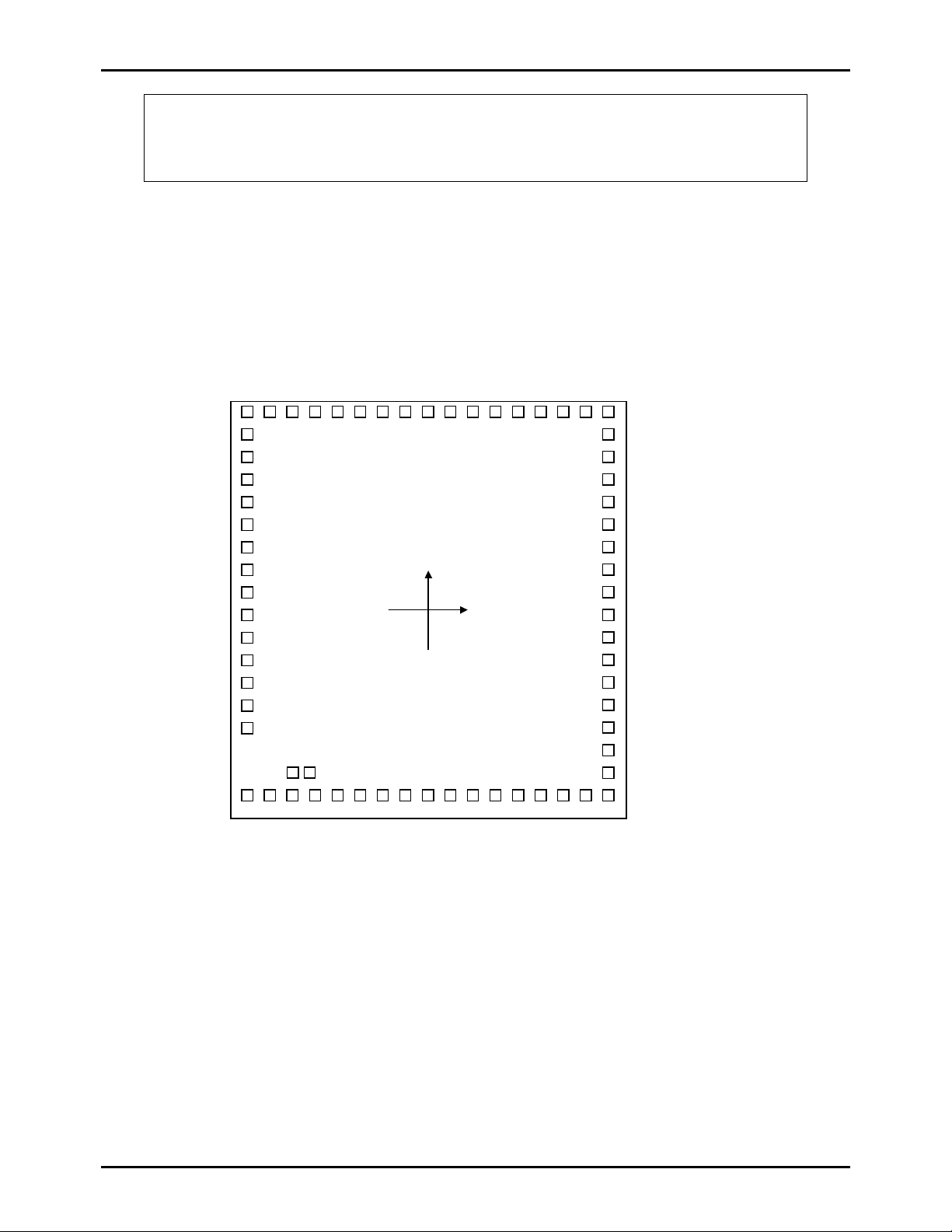
Pad assignment
Chip size (X × Y) : 2.6 3mm × 2.89mm
Chip thickness : 480µm
Pad size : 116µm × 116µm
LIGHT
ALM
VDD2
VDD1
BAK
S4
S3
P10
P11
P12
P13
P00
P01
P02
P03
COM3
SEG16
61
60 59 58 57 56 55 54 53 52 51 50 49 48 47 46
62
63
64
1
2
3
4
5
6
7
8
9
10
11
12 13 14 15 16 17 18 19 20 21 22 23 24 25 26 27
COM3
SEG17
SEG18
SEG15
SEG19
SEG14
SEG20
SEG13
SEG21
SEG12
SEG22
SEG11
SEG23
SEG10
Y
SEG24
LC573914
[Note]
SEG9
SEG8
X
SEG25
SEG26
SEG7
SEG6
SEG5
SEG4
SEG3
SEG2
45
SEG1
44
COM2
43
TEST
42
RCOUT
41
RCIN
40
VSS
39
OSCOUT
38
OSCIN
37
RES
36
S1
35
S2
34
32HZ
33
T3
32
CUP2
31
CUP1
30
COM1
29
SEG32
28
SEG27
SEG28
SEG29
SEG30
SEG31
No.6745-3/13
Page 4
LC573914
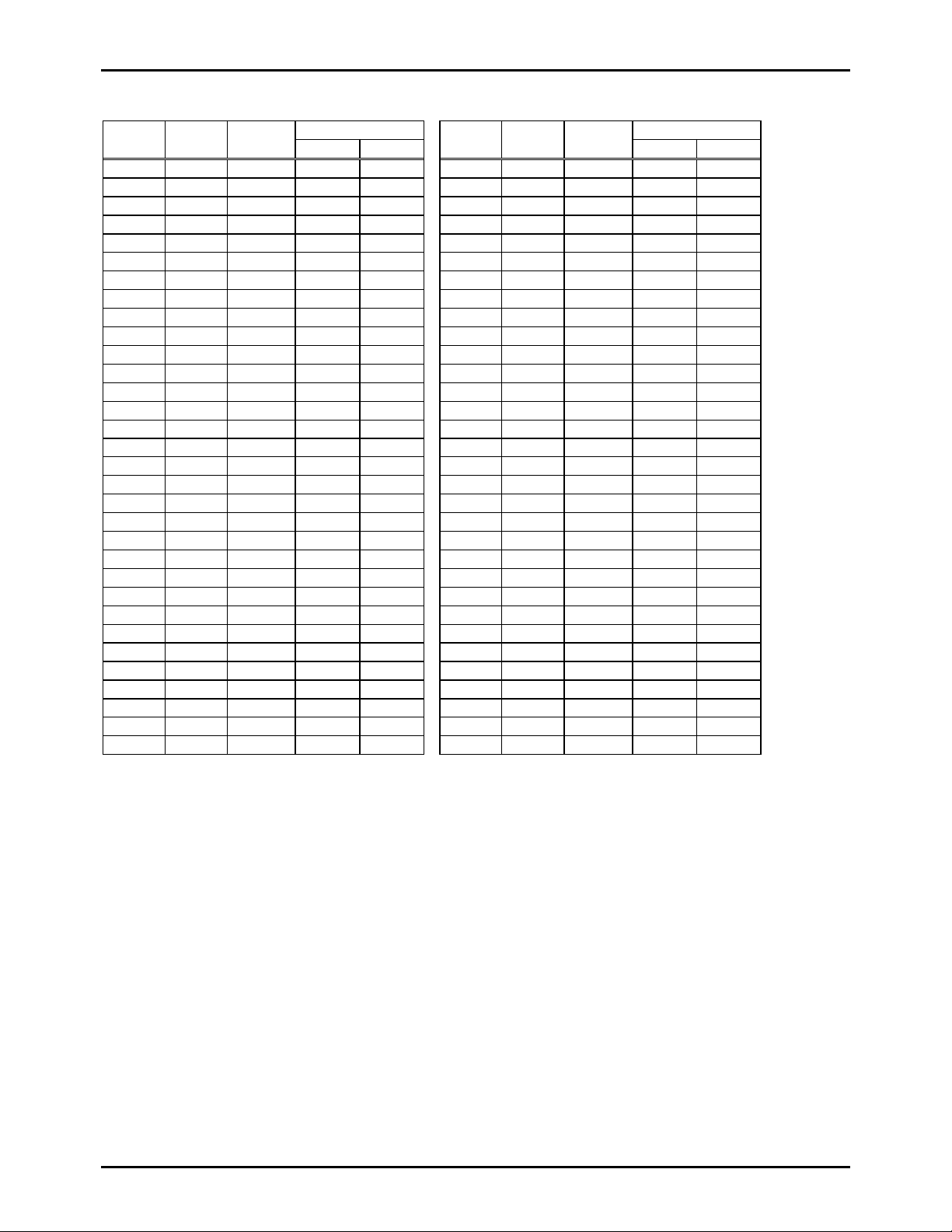
Pad name and coordinates
Pad
PIN No.
5 1 BAK -1065 645 37 33 32HZ 1065 -505
6 2 S4 -1065 455 38 34 S2 1065 -380
7 3 S3 -1065 330 39 35 S1 1065 -255
8 4 P10 -1065 170 40 36 RES 1065 -130
9 5 P11 -1065 5 41 37 OSCIN 1065 -5
10 6 P12 -1065 -155 42 38 OSCOUT 1065 115
11 7 P13 -1065 -315 43 39 VSS 1065 300
12 8 P00 -1065 -475 44 40 RCIN 1065 490
13 9 P01 -1065 -635 45 41 RCOUT 1065 615
14 10 P02 -1065 -800 46 42 TEST 1065 740
15 11 P03 -1065 -960 47 43 COM2 1065 865
16 12 COM4 -1080 -1205 48 44 SEG1 1065 1005
17 13 SEG17 -940 -1205 49 45 SEG2 1075 1205
18 14 SEG18 -790 -1205 50 46 SEG3 935 1205
19 15 SEG19 -650 -1205 51 47 SEG4 810 1205
20 16 SEG20 -525 -1205 52 48 SEG5 685 1205
21 17 SEG21 -400 -1205 53 49 SEG6 560 1205
22 18 SEG22 -275 -1205 54 50 SEG7 435 1205
23 19 SEG23 -150 -1205 55 51 SEG8 310 1205
24 20 SEG24 -25 -1205 56 52 SEG9 185 1205
25 21 SEG25 100 -1205 57 53 SEG10 60 1205
26 22 SEG26 225 -1205 58 54 SEG11 -65 1205
27 23 SEG27 350 -1205 59 55 SEG12 -190 1205
28 24 SEG28 475 -1205 60 56 SEG13 -315 1205
29 25 SEG29 600 -1205 61 57 SEG14 -440 1205
30 26 SEG30 725 -1205 62 58 SEG15 -565 1205
31 27 SEG31 865 -1205 63 59 SEG16 -705 1205
32 28 SEG32 1065 -1185 64 60 COM3 -855 1205
33 29 COM1 1065 -1035 1 61 LIGHT -1065 1195
34 30 CUP1 1065 -895 2 62 ALM -1065 1070
35 31 CUP2 1065 -770 3 63 VDD2 -1065 895
36 32 T3 1065 -630 4 64 VDD1 -1065 770
No.
Pad
Name
The pad coordinates are such that the chip center is taken as the origin and the values for (X, Y) represent the coordinates of
the center point of each pad.
Substrate must be connected to VSS or left open.
Coordinates Coordinates QFP64
Xµm Yµm
QFP64
PIN No.
Pad
No.
Pad
Name
Xµm Yµm
No.6745-4/13
Page 5

Package Dimension
T
K
(unit : mm)
3159
Pin Assignment QIP64E
SEG2
SEG3
SEG4
SEG5
SEG6
SEG7
SEG8
SEG9
SEG10
SEG11
SEG12
SEG13
SEG14
SEG15
SEG16
COM3
49
50
51
52
53
54
55
56
57
58
59
60
61
62
63
64
LC573914
SEG1
COM2
TEST
RCOUT
RCIN
VSS
OSCOUT
OSCIN
RES
S1
S2
32HZ
T3
CUP2
CUP1
COM1
48 47 46 45 44 43 42 41 40 39 38 37 36 35 34 33
1 2 3 4 5 6 7 8 9 10 11 12 13 14 15 16
S4
S3
P10
P11
P12
P13
P00
P01
P02
LIGH
ALM
BA
VDD2
VDD1
P03
COM4
32
31
30
29
28
27
26
25
24
23
22
21
20
19
18
17
SANYO : QIP-64E
SEG32
SEG31
SEG30
SEG29
SEG28
SEG27
SEG26
SEG25
SEG24
SEG23
SEG22
SEG21
SEG20
SEG19
SEG18
SEG17
No.6745-5/13
Page 6

System Bl ock Diagram
HALT mode control
Stand-by c ontr ol
RC
Clock generator
Base timer
Chronograph counter
Melody/buzzer
circuit
Strove pointer
SEGMENT PLA
LCD driver
S port
LC573914
IR PLA
ROM
PC
circuit
Control
Stack
AC
ALU
TMP
DPL DPH
RAM
P0 port
P1 port
No.6745-6/13
Page 7

LC573914
Sample Application Circuit
(1) Ag battery used application (1/2 bias 1/4 duty)
KEY MATRIX
0.1µF
P00
P01
P02
P03
P10
P11
P12
P13
S1
S2
S3
S4
OSCIN
OSCOUT
RES
RCIN
RCOUT
COM1
COM2
COM3
COM4
SEG1-32
VDD1
VSS
VDD2
CUP1
CUP2
ALM
LIGHT
0.1µF
0.1µF
1.5V(Ag)
LCD GLASS
1/2 BIAS
1/4 DUTY
(Power supply : Ag battery version)
Note 1) If P0, P1 port or segment output (SEG17 to SEG32) are used for key scan output port, P-ch open drain option should
be used in order to prohibit signal short between output ports when two or more keys are pushed simultaneously.
Note 2) If P1 port is used as output port, the following setting is necessary. Programmable pull-down resistors which is one
of the internal pull-down register should be set to open mode with the SPDR instruction.
No.6745-7/13
Page 8

LC573914
LC573904 Terminal Description
Name
VSS 43 39 - Power terminal (-)
VDD1 9 64 - •Power terminal(+) (Ag battery version)
VDD2 3 63 - •Voltage suppl y to LCD dr iver (Ag battery version)
BAK 5 1 - •Power terminal(+)
CUP1,2 34
S port
S1-S4
P1 port
P10-P13
P0 port
P00-P03
LIGHT 1 61 O Output port
ALM 2 62 O •Output port
SEG1
-SEG32
COM1
-COM4
OSCIN 41 37 I This terminal should be connected with RCOUT.
OSCOUT 42 38 O This terminal should be left unconnected.
Pin
No.
8-11 4-7 I/O •4-bit input/output port
12-15 8-11 I/O •4-bit input/output port
48-63
17-32
35
39
38
7
6
33
47
64
16
PAD
No.
30
31
35
34
3
2
44-59
13-28
29
43
60
12
I/O Function description Option
Battery version
Voltage supply to logic unit (Ag battery version)
•
(C is connected between VDD2 an d VSS.)
Capacitor is required between BAK and VSS
•
- Capaci tor connecting terminals for step-up
I •4-bit input port
Input for HALT release
•
LSI system is reset by applying VDD to S1 to S4
•
simultaneously.
Programmable pull-dow n res istor
•
”L”-level hold Tr.
•
CMOS output/P-ch open drain output
•
Input for HALT release
•
Programmable pull-down resistor
•
”L”-level hold Tr.
•
”H”-level hold Tr.
•
CMOS output/P-ch open drain output
•
”H”-level hold Tr.
•
Output terminal to deliver melody signal or buzzer
•
with SAS or TMEL instruction.
(Buzzer : modulation signal or non modulati on
signal.)*
(Melody signal : 3 octaves)
O •LCD output terminals for segment
Possible to use output port for SEG17 to SEG32
•
(Pad No.13 to 28) by mask option.
O LCD output terminals for common LCD duty
Ag
Battery version
Ag
”L”-level hold Tr.
Provided/Not provided
”L”-level hold Tr.
•
Provided/Not provided
”H”-level hold Tr.
•
Provided/Not provided
Output form CMOS
•
/P- ch open drain
”H”-level hold Tr.
•
Provided/Not provided
Output form CMOS
•
/P- ch open drain
Output form
•
segment/CMOS/P ch open drain
Segment data
•
SP=0 - FH
DBUS=a/b/c/d/e/f
/g/h
1/1,1/2,1/3,1/4
Continue.
No.6745-8/13
Page 9

LC573914
Name
RCIN 44 40 I •Input for RC oscillation
RCOUT 45 41 O •Output for RC oscillation
RES 40 36 I Reset
32HZ 37 33 - •Test terminal
T3 36 32 - •Test terminal
TEST 46 42 - •Test terminal
Pin
No.
PAD
No.
I/O Function description Option
R is connected across RCIN and RCOUT, and C is
connected across RCIN and VSS.
R is connected across RCIN and RCOUT.
This terminal should be left unconnected.
This terminal should be left unconnected.
This terminal should be left unconnected.
No.6745-9/13
Page 10

LC573914
Ag battery version
1. Absolute Maximum Ratings at Ta=25±2°C, VSS=0V
Parameter Symbol Pin & Conditions Ratings Unit
VDD1 -0.3 to +4.0 Supply voltage
VDD2 -0.3 to +4.0
Input voltage VIN S1-S4, P00-P03, P10-P13, TEST,
OSCIN, RES, RCIN
VOUT1 CUP2, OSCO UT, ALM, LIGHT,
P00-P03, P10-P13, RCOUT
VOUT2 SEG1-SEG32, COM1-COM4, CUP1 -0.3 to VDD2+0 .3
Peak output
current
(at each pins)
Total output
current
Maximum power
dissipation
Operating
temperature
range
Storage
temperature
range
IOUT1 ALM 4
IOUT2 LIGHT 1
IOUT3 Output ex c e pt ALM and LIGHT 500
IALL Total output pins. 10 mA
Pdmax QFP64 430 mW
Topr -30 to +70
Tstg -40 to +125
2. Recommended Operating Range at Ta=-30°C to + 70°C, VSS=0V
Parameter Symbol Conditions
VDD1 1.20 1.65 Operating supply
voltage
Input high voltage VIH S1-S4, RES,
Input low voltage VIL S1-S4, RES,
Oscillation
frequency range
VDD2 2.4 3.3
VDD1-0.2 VDD1
P00-P03, P10-P13
P00-P03, P10-P13
fOPG2 •RC oscillation
•VDD1=1.20 - 1.65V (Ta=25°C)
•Refer to figure 2
min. typ. max.
-0.3 to VDD1+0.3
-0.3 to VDD1+0.3 Output voltage
Ratings
0 0.2
30 190 kHz
V
mA
A
µ
C
°
Unit
V
No.6745-10/13
Page 11

LC573914
3. Electrical Characteristics at Ta=-30°C to + 70°C, VSS=0V
Parameter Symbol Conditions
Pull-down transistor
RIN1A VDD1=1.55V, VIL=0.2V,
Low level hold Tr. Fig.3 *1
RIN1B VDD1=1.55V,
Low level pull in Tr. Fig.3 *1
RIN3 VDD1=1.55V, TEST, RES 10 300
Pull-up transistor RIN2 VDD1=1.55V,
High level hold Tr. Fig.6 *5
Output high voltage VOH1 V DD1=1 .55V, IOH=-0.4µA *2
VDD2-0.2
Output low voltage VOL1 VDD1=1.55V, IOL=0.4µA *2 0.2
Output high voltage VOH2 V DD1=1 .55V, IOH=-4µA, COM1-4
Output middle voltage VOM VDD1=1.55V, IOH=-4µA, IOL=4µA,
VDD2-0.2
VDD1-0.2
COM1-4
Output low voltage V OL2 VDD1=1.55V, IOL=4µA, COM1-4
Output high voltage VOH3 VDD1=1.35V, IOH=-250µA, ALM,
VDD1-0.65
LIGHT
Output low voltage VOL3 VDD1=1.35V, IOL=150µA, ALM, LIGHT
Output high voltage VOH4 V DD1=1 .55V, IOH=-20µA *3
VDD1-0.2
Output low voltage VOL4 VDD1=1.55V, IOL=20µA *4 0.2
Output high curren t IOH VDD1=1 .55V, VOH=VDD1 × 0.5 *5 -100
Output low current IOL VDD1=1.55V, VOL=VDD1 × 0.5 *6 100
Step-up voltage VDD2 VDD1=1.35V, C1=C2=0 .1µF,
fopg=32.768kHz, Fig.4
Current dissipation
(In Halt mode)
IDD1
IDD2
VDD1=1.55V,
C1=C2=0.1µF, Fig.4,
RC osc(Rext=470 kΩ,
Cext=18pF),
Back-up flag OFF,
RC osc stop 0.01 1
RC osc
operating
Ta≤50°C
Current dissipation
(In operating mode)
IDD3
IDD4
VDD1=1.55V,
C1=C2=0.1µF, Fig.4,
RC osc(Rext=470 kΩ,
Cext=18pF),
RC osc
operating
Back-up flag OFF,
Ta≤50°C
Ratings
min. typ. max.
150 300 1000
Unit
kΩ
100 300 500
100 400 2000
V
VDD1+0.2
0.2
0.6
A
µ
2.5 2.7 V
A
µ
5.0 15.0
7.0 20.0
No.6745-11/13
Page 12

LC573914
RCIN RCOUT
Rext
Cext
VSS
Program-applied
VSS
Figure 2 RC oscillation circuit Figure 3 Input configuration of S1-4, P10-13
0.1µF
Cext
Rext
CUP1
CUP2
RCIN
RCOUT
VSS
DUT
OSCIN
OSCOUT
VDD1
VDD2
0.1µF
VDD1
Figure 4 Current dissipation, step-up voltage Figure 6 I nput configuration of P00-03, P10-13
measurement
[Note]
The specifications above are for a die mounted in a QFP64 type package. The specifications for a die is almost
same as ones for a QFP type package basically. However, the operational characteristics may vary depending
on the user’s assembling method. Therefore, the operating temperature range for a die is specified only in
Ta=25°C±2°C.
No.6745-12/13
Page 13

LC573914
No.6745-13/13
PS
 Loading...