

Page 1

Any and all SANYO products described or contained herein do not have specifications that can handle
applications that require extremely high levels of reliability, such as life-support systems, aircraft’s
control systems, or other applications whose failure can be reasonably expected to result in serious
physical and/or material damage. Consult with your SANYO representative nearest you before using
any SANYO products described or contained herein in such applications.
SANYO assumes no responsibility for equipment failures that result from using products at values that
exceed, even momentarily, rated values (such as maximum ratings, operating condition ranges,or other
parameters) listed in products specifications of any and all SANYO products described or contained
herein.
CMOS IC
4-Bit Single Chip Microcontroller
with LCD Drivers
for Low-Voltage, Low Power Use
Ordering number:ENN3540
LC5738
SANYO Electric Co.,Ltd. Semiconductor Company
TOKYO OFFICE Tokyo Bldg., 1-10, 1 Chome, Ueno, Taito-ku, TOKYO, 110-8534 JAPAN
Overview
The LC5738 is a single-chip 4-bit microcontroller with LCD
drivers. The features of the LC5738 include low voltage
operation, low power dissipation, etc. The HALT function,
which can be used to stop/start the CPU operations, facilitates the low power dissipation of the system. The LC5738
is ideally suited for use in melody function-provided timepiece/timer, game, functional watch and calculator application.
Package Dimensions
unit:mm
3159-QIP64E
[LC5738]
17.2
14.0
0.8
0.35
17.2
1.0
48
1.0
1.6
49
14.0
1.6
1.0
33
32
0.15
Hardware Features
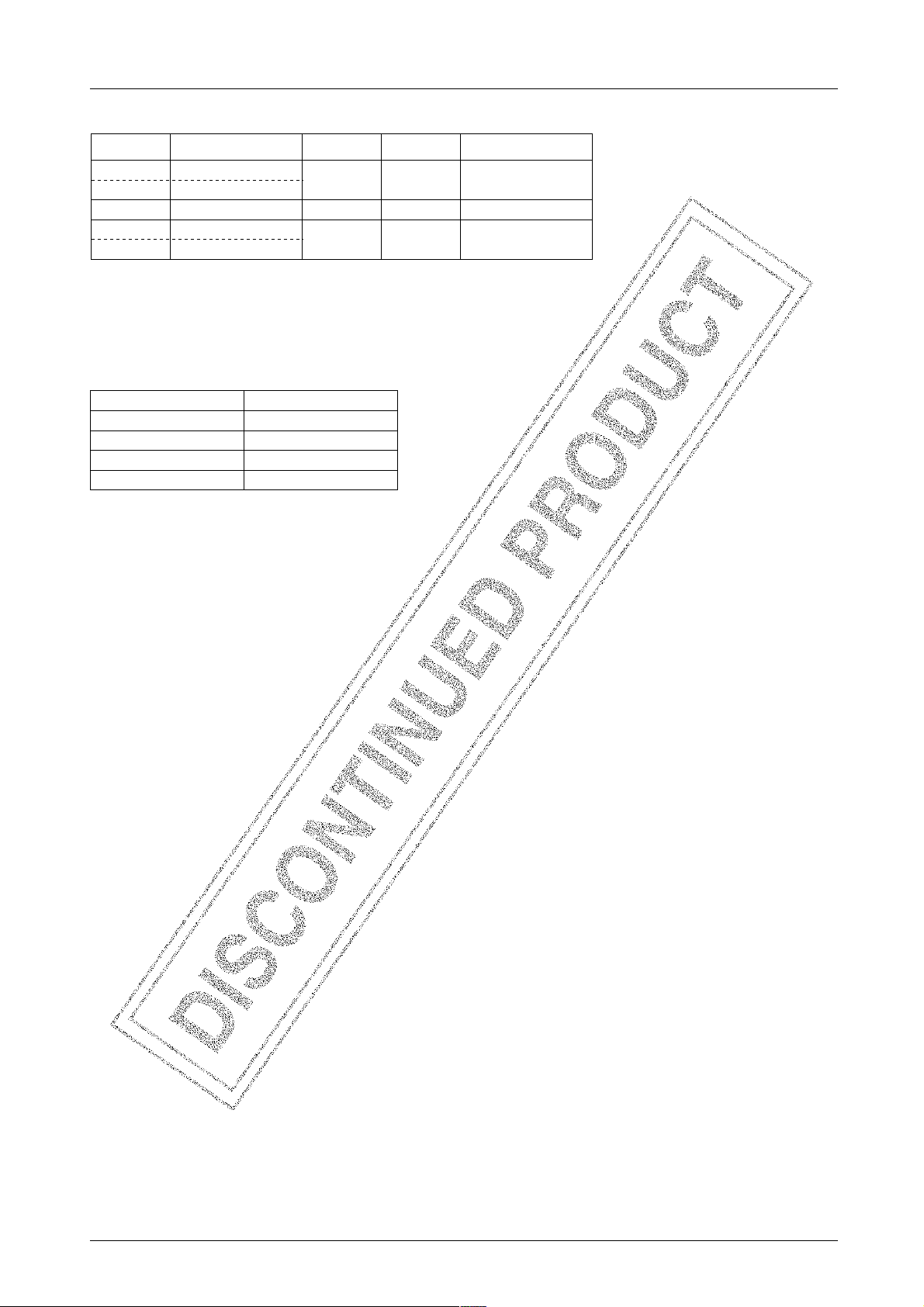
• ROM ......4096×8bits
• RAM .......... 40×4bits
• Cycle time
Cycle time
122µs 32.768kHz 1.30 to 1.65V
122µs 32.768kHz 2.60 to 3.60VX'tal oscillation Li battery version
122µs 32.768kHz 2.00 to 3.60V
System clock source Remarks
X'tal oscillation
RC oscillation
X'tal oscillation
RC oscillation
Oscillation
frequency
Operating
voltage range
Ag battery version
EXT-V version
• Current drain
a. Basic system operation mode
Current
drain
2.5µA typ.
10µA typ.
2.0µA typ. 32.768kHz 2.90VX'tal oscillation Li battery version
6.0µA typ.
50µA typ.
System clock source Remarks
X'tal oscillation
RC oscillation
X'tal oscillation
RC oscillation
Oscillation
frequency
32.768kHz 1.55V
32.768kHz 2.90V
Operating
voltage range
Ag battery version
EXT-V version
0.8
64
1.0
1
15.6
17
16
0.1
3.0max
2.7
0.8
SANYO : QIP64E
72501TN (KT)/5100TA/4060TA, TS No.3540–1/12
Page 2
LC5738
b. HALT operation mode
Current
drain
1.0µA typ.
5.0µA typ.
0.8µA typ. 32.768kHz 2.90VX'tal oscillation Li battery version
3.0µA typ.
40µA typ.
System clock source Remarks
X'tal oscillation
RC oscillation
X'tal oscillation
RC oscillation
• Ports
- Input ports : 2 ports (8 pins)
• Control output pins 3 pins
- Output dedicated to alarm 2 pins
- General purpose output 1 pin
• LCD drivers
edomyalpsidDCLstnemgeselbavirdforebmuN
saibcitatS·ytudcitatSstnemges23
saib2/1·ytud2/1stnemges46
saib2/1·ytud3/1stnemges69
saib2/1·ytud4/1stnemges821
• Possible to use LCD drive output pins as output ports (Max. 16 pins. mask option selectable)
• On-chip melody function ........3 octaves × 2 channels
• On-chip segment PLA
The LCD driver can be used to support any LCD pannel layout without software processing.
• On-chip step-up/step-down circuit.
• Shipping style : chip or FLP-64
Note) When mounting the QIP package on the board, do not dip it in solder.
Oscillation
frequency
32.768kHz 1.55V
32.768kHz 2.90V
Operating
voltage range
Ag battery version
EXT-V version
Software Features
• Powerful instruction set : 92 instructions
• Table read instruction (possible to set table in all ROM areas).
• 1 subroutine stack level.
• 15 bits time base timer.
- Deliver and overflow signal every 32ms or 64ms, 100ms and 500ms.
• HALT function.
Development Support System
The development support system for the LC5738 applications consists of the following support tools :
(1) Manual
(a) User’s Manual : LC5738 user’s manual
(b) Tool Manual : LC5738 tool manual
(2) Development support tools
(a) Tools for developing the LC5738 application programs.
- MS-DOS machine
- Assembler (LC5738. EXE)
- Mask option selections program (SU5738. EXE)
(b) Tools for evaluating the LC5738 application systems.
- Evaluation chip : LC5797
Note 1) Since the evaluation chip LC5797 differs LC5738 with RAM capacity, be sure to check the RAM capacity
when preparing or debugging programs.
LC5738 : 48×4 bits, LC5797 : 256×4 bits
Note 2) When dev eloping pro grams, tak e care of the DPH value. The usable DPH v alues are 0 to 2 ex cept ROM bank
selection.
We will be free from any blame even if you use DPH=3 to FH for RAM addressing.
- Evaluation chip board : TB5738
Note) The application evaluation board is constructed by the user.
LCD or LEDs may be used for display.
- Evaluation board : EVA520 (monitor ROM : SCR5738)
Note) The EVA-520 is a modified version of the EVA-420 whose monitor ROM is replaced by the SCR-5738.
- Display and mask-option data control board : DCB-1 (Rev.3.3)
No.3540–2/12
Page 3
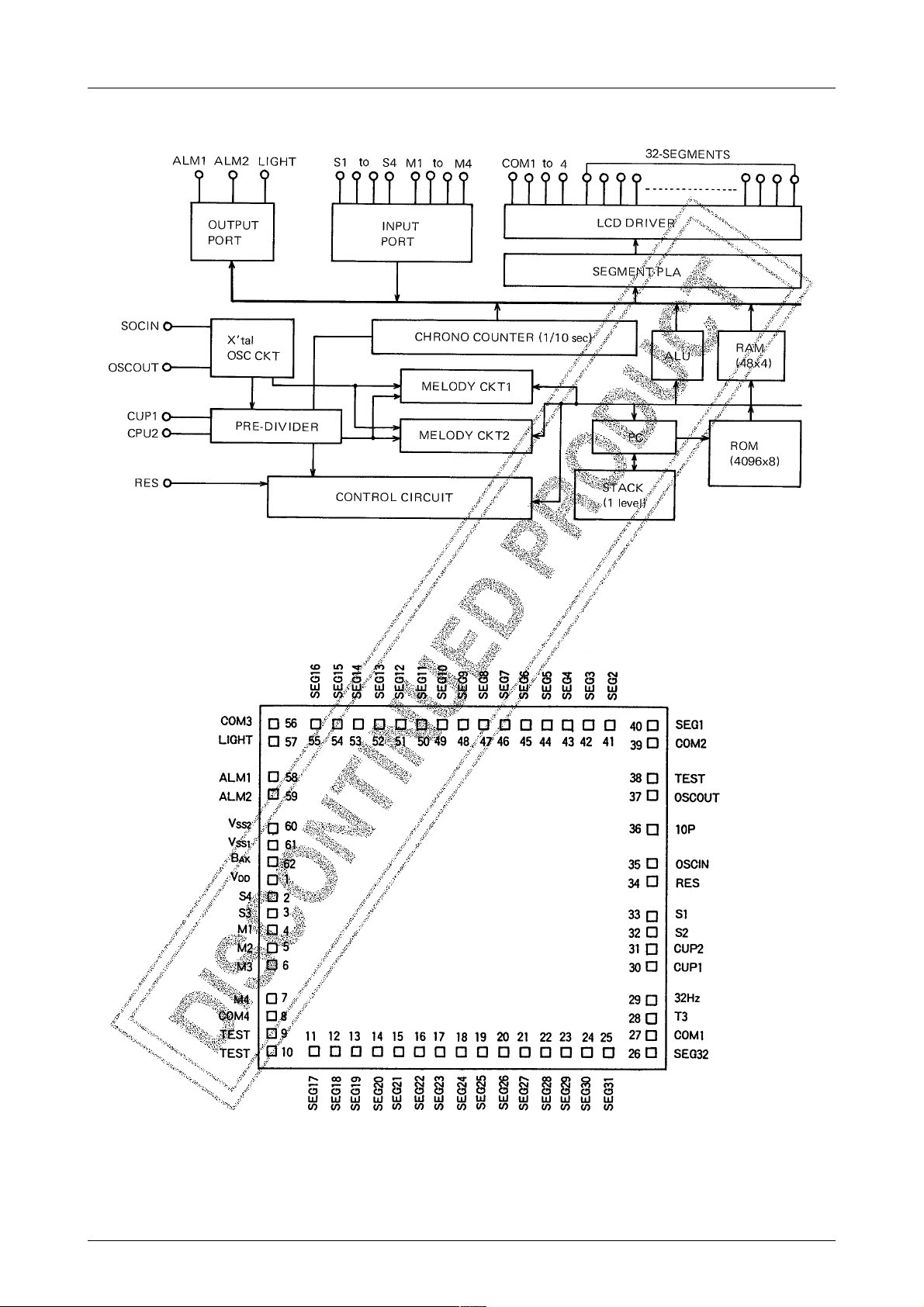
Equivalent Circuit and Block Diagram
LC5738
Pad Assignment of IC Chip
Chip size : 3.85mm×3.75mm
Chip thickness : 480µm
Pad size : 120µm×120µm
Note) SEG17 to 32 can be used for output ports. (Mask option-selectable)
No.3540–3/12
Page 4
Pad Name and Coordlinates
QIP64 Pin Assignment
Pad
No.
55
1
10
11
12
13
14
15
16
17
18
19
20
21
22
23
24
25
26
27
28
29
30
31
32
33
34
35
2
3
4
5
6
7
8
9
V
S4
S3
M1
M2
M3
M4
TEST
TEST
COM14
SEG17
SEG18
SEG19
SEG20
SEG21
SEG22
SEG23
SEG24
SEG25
SEG26
SEG27
SEG28
SEG29
SEG30
SEG31
SEG32
COM1
T3
32Hz
CUP1
CUP2
S2
S1
RES
OSCIN
56
57
58
59
60
61
62
63
64
1
2
3
4
5
6
7
8
9
10
11
12
13
14
15
18
19
20
21
22
23
24
25
26
27
Pin
Name
DD
X
(µm)Y(µm)
–1725
–1725
–1725
–1725
–1725
–1725
–1725
–1725
–1725
–1725
–1430
–1220
–1010
– 800
– 590
– 380
– 170
240
450
660
870
1080
1290
1500
1730
1730
1730
1730
1730
1730
1730
1730
1730
1730
– 125
– 360
– 575
– 805
–1030
–1260
–1485
–1675
–1675
–1675
–1675
–1675
–1675
–1675
–1675
40
–1675
–1675
–1675
–1675
–1675
–1675
–1675
–1675
–1675
–1435
–1185
– 940
– 695
– 455
– 215
335
115
30
245
565
QIP64 Pin Assignment
Pad
No.
28
36
37
38
39
40
41
42
43
44
45
46
47
48
49
50
51
52
53
54
55
56
57
58
59
60
61
62
10P
OSCOUT
TEST
COM2
SEG1
SEG2
SEG3
SEG4
SEG5
SEG6
SEG7
SEG8
SEG9
SEG10
SEG11
SEG12
SEG13
SEG14
SEG15
SEG16
COM3
LIGHT
ALM1
ALM2
VSS2
VSS1
BAK
29
30
31
32
33
34
35
36
37
38
39
40
41
42
43
44
45
46
47
48
49
50
51
52
53
54
LC5738
Pin
Name
X
(µm)Y(µm)
1730
1730
1730
1730
1730
1425
1225
1020
815
610
405
210
10
– 195
– 400
– 605
– 810
–1010
–1215
–1420
–1725
–1725
–1725
–1725
–1725
–1725
–1725
775
990
1255
1470
1675
1675
1675
1675
1675
1675
1675
1675
1675
1675
1675
1675
1675
1675
1675
1675
1675
1495
1280
1090
905
725
545
• The pad coordinates are such that the chip enter is taken as the origin and the values for (X, Y) represent the coordinates
of the center point of each pad.
• Pin 16, 17 are NC pins.
• The NC pins must not be connected externally.
No.3540–4/12
Page 5

Pin Description
daP
.oN
niP
emaN
LC5738
/tupnI
tuptuO
noitarugifnoCtiucriCnoitcnuF
53NICSOtupnI
73TUOCSOtuptuO
63P01 – .roticapacnoitasnepmocesahpCSOsadesudnaTUOCSOotdetcennoC
33
1S
23
2S
3
3S
2
4S
4
1M
5
2M
6
3M
7
4M
43SERtupnI .metsysCIgnitteserrofniptupnI
tupnI
tupnI.tropylno-tupnI
.edomCSOlatsyrC
edomCSOCR
.kcolcmetsyssadesU
.tropylno-tupnI
VgniylppaybtesersimetsysCI
DD
.kcolcmetsysdnaeceipemitrofkcolcecnerefersadesU
.ylsuoenatlumis4Sot1Sot
.noitallicsorofTUOCSOdnaNICSOssorcadetcennocsilatsyrczHk867.23
.noitallicsorofTUOCSOdnaNICSOssorcadetcennoceraCdnaR
26KAB –
75THGILtuptuO
851MLAtuptuO
952MLAtuptuO
.CIehtedisnitinucigolrofnipylppusrewop)–(
.gninoitcnuflammorftinucigoltneverp
.nipylno-tuptuO
.thgilrofrotsisnartevirdotlangisgnireviledrofdetiuS
.nipylno-tuptuO
)langisnoitaludom-nonreviledotdesuoslA(
.nipylno-tuptuO
)langisnoitaludom-nonreviledotdesuoslA(
VdnaKABssorcadetcennocebtsumroticapaca,noisrevyrettabiLroF
ot
DD
3folangisydolemreviledotdesu,2-lennahcydolemgnitcelesfoesacnI
.snoitcurtsniLEMTroSAShtiwlangisnoitaludomzHk1/zHk2/zHk4*rosevatco
3folangisydolemreviledotdesu,2-lennahcydolemgnitcelesfoesacnI
.snoitcurtsniLEMTroSAShtiwlangisnoitaludomzHk1/zHk2/zHk4*rosevatco
Continued on next page.
No.3540–5/12
Page 6

Continued from preceding page.
daP
.oN
1V
niP
emaN
DD
– .nipylppusrewop)+(
LC5738
/tupnI
tuptuO
noitarugifnoCtiucriCnoitcnuF
.nipylppusrewop)–(
.noisrevV-TXEyrettabiL/yrettabgA:elbatcelesnoitpoksaM
.evirdDCLrofylppusrewopsadesuoslA
.esachcaenistraplanretxetcennocotwohswohselbaTgniwollofehT
1606VSS1
VSS2
03
13
72
93
65
01
62ot11
55ot04
92
3T
82
8
9
83
–
1PUC
2PUC
1MOC
2MOC
3MOC
4MOC
23GES
61GES
zH23
TSET
TSET
TSET
– .roticapac)nwod-pets(pu-petsegatlovgnitcennocrofsniP
tuptuO
ot71GES
ot1GES
tuptuO
tseT)resuybdesuton(sniptseT
Duty mode
COM1
COM2
COM3
COM4
Alternating
frequency
.strop
.esachcaenidesusisnipgniwollofehT
Static 1/2 1/3 1/4
°
°
°
°
–
°
––
–––
64Hz 32Hz 43Hz 32Hz
°
°
°
°
°
.stnemgeslennapDCLrofsniptuptuO
.etalpnommoclennapDCLrofsniptuptuO
tuptuosadesuebot)62ot11.oNdap(23GESot71GESstimrepnoitpoksaM
Note) For Ag battery power supply, is connected to VSS1 ; for Li battery/EXT-V power supply, connected to VSS2.
* 4kHz/2kHz/1kHz : For 32.768kHz crystal OSC application, proportional to OSC frequency.
No.3540–6/12
Page 7

LC5738
Sample Application Circuits
(1) Ag battery used application (1/2bias 1/4 duty) (2) Li battery used application (1/2bias 1/4duty)
* : 4 segment outputs are used for output ports. * : 4 segment outputs are used for output ports.
Crystal OSC Crystal OSC
(power supply : Ag battery version) (power supply : Li battery version)
(3) EXT-V used application (1/2bias 1/4 duty)
* : 4 segment outputs are used for output ports.
Crystal OSC (power supply : EXT-V version) Unit (capacitance : F)
No.3540–7/12
Page 8

LC5738
Specifications
Ag Battery Version
Absolute Maximum Ratings at Ta = 25±2˚C, V
retemaraPlobmySsnoitidnoCsgnitaRtinU
egatlovylppuS
egatlovtupnIV
egatlovtuptuO
tnerructuptuO
)niprep(
tnerructuptuOI
erutarepmetgnitarepOrpoT 07+ot03–
erutarepmetegarotSgtsT 521+ot04–
VSS1 3.0+ot0.4– V
VSS2 3.0+ot0.4– V
1SER,NICSO,p01,TSET,zH23,4M-1M,4S-1SV
NI
V
1TUO
V
2TUO
I
12MLA,1MLA 4Am
TUO
I
2THGIL2 1Am
TUO
I
3THGILdna2,1MLAtpecxestuptuO 005Aµ
TUO
LLA
Recommended Operating Voltage Range at Ta = –30 to +70˚C, VDD=0V
retemaraPlobmySsnoitidnoC
egnaregatlovylppusgnitarepO
egatlovlevel-hgihtupnIV
egatlovlevel-woltupnIV
egnarycneuqerfnoitallicsO
VSS156.1– 03.1– V
VSS23.3– 4.2– V
HI
LI
f
11.giFnoitallicsolatsyrC23867.2333zHk
GPO
f
2k074=txeR,2.giF,noitallicsoCR Ω Fp03=txeC,867.23zHk
GPO
DD
=0V
tnerructuptuolatoT 01Am
SER,4Mot1M,4Sot1S2.0– 0V
SER,4Mot1M,4Sot1SV
THGIL,2MLA,1MLA,TUOCSO,2PUC,zH23V
1PUC,4MOC,3MOC,2MOC,1MOC,TUOGESV
nimpytxam
SS
SS
SS
SS
sgnitaR
1VSS2.0+1V
3.0+ot3.0–1V
3.0+ot3.0–1V
3.0+ot3.0–2V
˚C
˚C
tinU
Electrical Characteristics at Ta =–30 to +70˚C, VDD=0V
retemaraPlobmySsnoitidnoC
V
RNIA1
rotsisnartnwod-lluP
egatlovlevel-HtuptuOV
egatlovevel-LtuptuOV
egatlovlevel-HtuptuOV
egatlovlevel-MtuptuOV
egatlovlevel-LtuptuOV
egatlovlevel-HtuptuOV
egatlovlevel-LtuptuOV
egatlovlevel-HtuptuOV
egatlovlevel-LtuptuOV
egatlovtuptuOV
edomTLAHniniardtnerruC
noitarepocisabgnirudniardtnerruC
egatlovtratsnoitallicsOV
egatlovdlohnoitallicsOV
emittratsnoitallicsOt
ecnaticapacnoitasnepmocnoitallicsOP01niplanretxE80121Fp
RNIB1V
RNI2V
HO
LO
HO
MO
LO
HO
LO
HO
LO
SS
IDD1
IDD2
IDD3
IDD4
tts
SS
SS
SS
1V
SS
1V
SS
2V
SS
V
SS
2V
SS
V
SS
3
3V
4V
4V
2
tts
DLOH
THGIL
SS
SS
SS
V
SS
4.giF
V
SS
aT ≤ 05 °C
V
SS
aT ≤ 05 °C
V
SS
aT ≤ 05 °C
V
SS
aT ≤ 05 °C
V
SS
IC( ≤ k52 Ω 52=aT,tesergalf-pu-kcaB,) ° 6.giF,C
V,V55.1–=1
3.giF,1*
I,V55.1–=1
I,V55.1–=1
I,V55.1–=1
I,V55.1–=1
I,V55.1–=1
I,V53.1–=1
I,V53.1–=1
I,V55.1–=1
I,V55.1–=1
IC(CSOlatsyrC ≤ k52 Ω ,tesergalf-pu-kcaB,)
k074=txeR( Ω ,tesergalf-pu-kcaB,)Fp03=txeC,
IC(CSOlatsyrC ≤ k52 Ω ,tesergalf-pu-kcaB,)
k074=txeR( Ω ,tesergalf-pu-kcaB,)Fp03=txeC,
52=aT,teser ° 6.giF,C
52=aT,teser ° 6.giF,C
sgnitaR
nimpytxam
LIV=SS
SER,TSET,V55.1–=101003kΩ
HO
LO
HO
HO
LO
HO
LO
HO
LO
2*,Aµ4.0–=2.0– V
2*,Aµ4.0=V
4ot1MOC,Aµ4–=2.0– V
I,Aµ4–=
LO
4ot1MOC,Aµ4=V
3*,Aµ02–=2.0– V
3*,Aµ02=V
IC(CSOlatsyrC,Fp02=gC ≤ k52 Ω galf-pu-kcaB,)
IC(CSOlatsyrC,Fp02=gC ≤ k52 Ω galf-pu-kcaB,)
CSOlatsyrC,Fp02=gC,V53.1–=1
,rTdlohlevel'L',V2.0+1
3.giF,1*,rTni-lluplevel'L',V55.1–=10020002kΩ
4ot1MOC,Aµ4=V
,2MLA,1MLA,Aµ052–=
THGIL,2MLA,1MLA,Aµ051=
,zHk867.23=gpof,Fµ1.0=2C=1C,V53.1–=1
,Fp02=gC,4.giF,Fµ1.0=2C=1C,V55.1–=1
CSOCR,5.giF,Fµ1.0=2C=1C,V55.1–=1
,Fp02=gC,4.giF,Fµ1.0=2C=1C,V55.1–=1
CSOCR,5.giF,Fµ1.0=2C=1C,V55.1–=1
0020002kΩ
2.0–1V
SS
56.0– V
3.3– 5.2– V
0.10.4Aµ
0.50.51Aµ
0.30.21Aµ
0.70.02Aµ
53.1– V
SS
SS
SS
V
SS
SS
tinU
2.0+2V
2.0+1V
2.0+2V
56.1+1
V
2.0+1V
03.1– V
01s
No.3540–8/12
Page 9

LC5738
Notes for developing an LC5730 series microcontroller-used system.
The low current drain is a distinctive feature of the LC5730 series microcontroller.
However, it is not easy to determine the total current reguired for LC5730 series microcontroller-used system by
actual measurement when you develop a software, bacause much current flows in the peripherals of the evaluation
tools.
For a system which requires low current drain, check the current drain using an evaluation sample before massproducting the system.
Li Battery Version
Absolute Maximum Ratings at Ta = 25±2˚C, V
retemaraPlobmySsnoitidnoCsgnitaRtinU
egatlovylppuS
egatlovtupnI
egatlovtuptuO
tnerructuptuO
)niprep(
tnerructuptuOI
erutarepmetgnitarepOrpoT 07+ot03–
erutarepmetegarotSgtsT 521+ot04–
VSS1 3.0+ot0.4– V
VSS2 3.0+ot0.4– V
VNI1NICSO,p01,zH23V
VNI2SER,TSET,4Mot1M,4Sot1SV
V
1TUO
V
2TUO
I
12MLA,1MLA 4Am
TUO
I
2THGIL 1Am
TUO
I
3THGILdna2,1MLAtpecxeniptuptuO 005Aµ
TUO
LLA
DD
=0V
1SS
TUOCSO,2PUC,zH23V
THGIL,2MLA,1MLA,1PUC,4MOCot1MOC,TUOGESV
tnerructuptuolatoT 01Am
2SS
1SS
2SS
3.0+ot3.0– V
3.0+ot3.0– V
3.0+ot3.0– V
3.0+ot3.0– V
˚C
˚C
Recommended Operating Voltage Range at Ta = –30 to +70˚C, VDD=0V
retemaraPlobmySsnoitidnoC
egnaregatlovylppusgnitarepO
egatlovlevel-hgihtupnIV
egatlovlevel-woltupnIV
egnarycneuqerfnoitallicsOf
VSS16.3– 03.1– V
VSS26.3– 0.2– V
HI
LI
11.giFnoitallicsolatsyrC23867.2333zHk
GPO
SER,4Mot1M,4Sot1S4.0– 0V
SER,4Mot1M,4Sot1SV
Electrical Characteristics at Ta =–30 to +70˚C, VDD=0V
retemaraPlobmySsnoitidnoC
V
RNIA1
rotsisnartnwod-lluP
egatlovlevel-HtuptuOV
egatlovevel-LtuptuOV
egatlovlevel-HtuptuOV
egatlovlevel-MtuptuOV
egatlovlevel-LtuptuOV
egatlovlevel-HtuptuOV
egatlovlevel-LtuptuOV
egatlovlevel-HtuptuOV
egatlovlevel-LtuptuOV
egatlovlevel-HtuptuOV
egatlovlevel-LtuptuOV
egatlovtuptuOV
edomTLAHniniardtnerruCI
noitarepocisabgnirudniardtnerruCI
RNIB1V
RNI2V
HO
LO
HO
MO
LO
HO
LO
HO
LO
HO
LO
SS
DD
DD
SS
SS
SS
1V
SS
1V
SS
2V
SS
V
SS
2V
SS
3V
SS
3V
SS
4V
SS
4V
SS
5V
SS
5V
SS
V
SS
1
V
SS
1
aT ≤ 05 °C
V
SS
2
aT ≤ 05 °C
8.giF
V,V9.2–=2
LIV=SS
7.giF,1*
7.giF,1*,rTni-lluplevel'L',V9.2–=20010002kΩ
SER,TSET,V9.2–=201003kΩ
I,V9.2–=2
HO
I,V9.2–=2
LO
I,V9.2–=2
HO
I,V9.2–=2
HO
I,V9.2–=2
LO
I,V4.2–=2
HO
I,V4.2–=2
LO
I,V4.2–=2
HO
I,V4.2–=2
LO
I,V9.2–=2
HO
I,V9.2–=2
LO
IC(CSOlatsyrC ≤ k52 Ω ,tesergalf-pu-kcaB,)
IC(CSOlatsyrC ≤ k52 Ω ,tesergalf-pu-kcaB,)
2*,Aµ4.0–=2.0– V
2*,Aµ4.0=V
4ot1MOC,Aµ4–=2.0– V
I,Aµ4–=
LO
4ot1MOC,Aµ4=V
2MLA,1MLA,Aµ052–=56.0– V
2MLA,1MLA,Aµ052=
THGIL,Aµ051–=5.1– V
THGIL,Aµ051=V
3*,Aµ04–=4.0– V
3*,Aµ04=V
sgnitaR
nimpytxam
2VSS4.0+2V
SS
sgnitaR
nimpytxam
,rTdlohlevel'L',V4.0+2
4ot1MOC,Aµ4=
,zHk867.23=gpof,Fµ1.0=2C=1C,V8.2–=2
,Fp02=gC,8.giF,Fµ1.0=2C=1C,V9.2–=2
,Fp02=gC,8.giF,Fµ1.0=2C=1C,V9.2–=2
0020002kΩ
V
2.0–2/2V
SS
8.00.2Aµ
5.10.5Aµ
SS
SS
SS
V
SS
SS
SS
tinU
tinU
2.0+2V
2.0+2/2
V
2.0+2V
56.0+2
V
5.1+2V
4.0+2V
53.1– V
Continued on next page.
No.3540–9/12
Page 10

Continued from preceding page.
retemaraPlobmySsnoitidnoC
egatlovtratsnoitallicsOV
egatlovdlohnoitallicsOV
emittratsnoitallicsOt
ecnaticapacnoitasnepmocnoitallicsOPO1niplanretxE80121Fp
tts
DLOH
V
tts
SS
IC( ≤ k52 Ω 52=aT,tesergalf-pu-kcaB,) ° 01.giF,C
EXT-V Version
Absolute Maximum Ratings at Ta = 25±2˚C, V
retemaraPlobmySsnoitidnoCsgnitaRtinU
egatlovylppuS
egatlovtupnIVNINICSO,p01,zH23,SER,TSET,4Mot1M,4Sot1SV
egatlovtuptuOV
tnerructuptuO
)niprep(
tnerructuptuOI
erutarepmetgnitarepOrpoT 07+ot03–
erutarepmetegarotSgtsT 521+ot04–
VSS1 3.0+ot0.4– V
VSS2 3.0+ot0.4– V
TUO
I
12MLA,1MLA 4Am
TUO
I
2THGIL 1Am
TUO
I
3THGILdna2,1MLAtpecxetuptuO 005Aµ
TUO
LLA
LC5738
52=aT,teser ° 01.giF,C
52=aT,teser ° 01.giF,C
=0V
DD
sgnitaR
nimpytxam
IC(CSOlatsyrC,Fp02=gC ≤ k52 Ω galf-pu-kcaB,)
IC(CSOlatsyrC,Fp02=gC ≤ k52 Ω galf-pu-kcaB,)
CSOlatsyrC,Fp02=gC,V53.1–=2
THGIL,2MLA,1MLA,TUOCSO
tnerructuptuolatoT 01Am
53.1– V
,2PUC,1PUC,zH23,4MOCot1MOC,TUOGES
V
3.1– V
01s
2SS
2SS
3.0+ot3.0– V
3.0+ot3.0– V
tinU
˚C
˚C
Recommended Operating Voltage Range at Ta = –30 to +70˚C, VDD=0V
retemaraPlobmySsnoitidnoC
egnaregatlovylppusgnitarepO
egatlovlevel-hgihtupnIV
egatlovlevel-woltupnIV
egnarycneuqerfnoitallicsO
VSS16.3– 03.1– V
VSS26.3– 0.2– V
HI
LI
f
11.giFCSOlatsyrC23867.2333zHk
GPO
f
2k074=txeR,Fp03=txeC,2.giF,CSOCR Ω 867.23zHk
GPO
SER,4Mot1M,4Sot1S4.0– 0V
SER,4Mot1M,4Sot1SV
Electrical Characteristics at Ta =–30 to +70˚C, VDD=0V
retemaraPlobmySsnoitidnoC
V
RNIA1
rotsisnartnwod-lluP
egatlovlevel-HtuptuOV
egatlovevel-LtuptuOV
egatlovlevel-HtuptuOV
egatlovlevel-MtuptuOV
egatlovlevel-LtuptuOV
egatlovlevel-HtuptuOV
egatlovlevel-LtuptuOV
egatlovlevel-HtuptuOV
egatlovlevel-LtuptuOV
egatlovlevel-HtuptuOV
egatlovlevel-LtuptuOV
egatlovtuptuOV
edomTLAHniniardtnerruC
RNIB1V
RNI2V
HO
LO
HO
MO
LO
HO
LO
HO
LO
HO
LO
SS
IDD1
IDD2
SS
SS
SS
1V
SS
1V
SS
2V
SS
V
SS
2V
SS
3V
SS
3V
SS
4V
SS
4V
SS
5V
SS
5V
SS
V
SS
1
V
SS
V
SS
8.giF
V,V9.2–=2
LIV=SS
7.giF,1*
SER,TSET,V9.2–=201003kΩ
I,V9.2–=2
HO
I,V9.2–=2
LO
I,V9.2–=2
HO
I,V9.2–=2
HO
I,V9.2–=2
LO
I,V4.2–=2
HO
I,V4.2–=2
LO
I,V4.2–=2
HO
I,V4.2–=2
LO
I,V9.2–=2
HO
I,V9.2–=2
LO
IC(CSOlatsyrC ≤ k52 Ω aT,) ≤ 05 °C
k=txeR( Ω, aT,)Fp03=txeC ≤ 05 °C
2*,Aµ4.0–=2.0– V
2*,Aµ4.0=V
I,Aµ4–=
LO
3*,Aµ04–=4.0– V
3*,Aµ04=V
7.giF,1*,rTni-lluplevel'L',V9.2–=20010002kΩ
4ot1MOC,Aµ4–=2.0– V
4ot1MOC,Aµ4=V
2MLA,1MLA,Aµ052–=56.0– V
2MLA,1MLA,Aµ052=
THGIL,Aµ051–=5.1– V
THGIL,Aµ051=V
sgnitaR
nimpytxam
2VSS4.0+2V
SS
sgnitaR
nimpytxam
,rTdlohlevel'L',V4.0+2
4ot1MOC,Aµ4=
,zHk867.23=gpof,Fµ1.0=2C=1C,V8.2–=2
,Fp02=gC,8.giF,Fµ1.0=2C=1C,V9.2–=2
CSOCR,9.giF,Fµ1.0=2C=1C,V9.2–=2
0020002kΩ
V
2.0–2/2V
SS
0.30.51Aµ
04051Aµ
SS
SS
SS
V
SS
SS
SS
tinU
tinU
2.0+2V
2.0+2/2
V
2.0+2V
56.0+2
V
5.1+2V
4.0+2V
53.1– V
Continued on next page.
No.3540–10/12
Page 11

LC5738
Continued from preceding page.
retemaraPlobmySsnoitidnoC
V
noitarepocisabgnirudniardtnerruC
egatlovtratsnoitallicsOV
egatlovdlohnoitallicsOV
emittratsnoitallicsOt
ecnaticapacnoitasnepmocnoitallicsOPO1niplanretxE80121Fp
IDD3
IDD4
tts
*1 : S1, S2, S3, S4, M1, M2, M3, M4.
*2 : SEGOUT1 to 16 and LCD output pins out of SEGOUT17 to 32.
*3 : OUTPUT PORT pins out of SEGOUT 17 to 32.
SS
V
SS
k074=txeR( ,Ω aT,)Fp03=txeC, ≤ 05 °C
tts
01
DLOH
01
V
SS
52=aT ° 01.giF,C
k52=IC(CSOlatsyrC Ω aT,) ≤ 05 °C
IC(CSOlatsyrC,Fp02=gC ≤ k52 Ω 52=aT,) ° .giF,C
IC(CSOlatsyrC,Fp02=gC ≤ k52 Ω 52=aT,) ° .giF,C
IC(CSOlatsyrC,Fp02=gC,V3.2–=2 ≤ k52 Ω ,)
sgnitaR
nimpytxam
,Fp02=gC,9.giF,Fµ1.0=2C=1C,V9.2–=2
CSOCR,9.giF,Fµ1.0=2C=1C,V9.2–=2
0.70.03Aµ
05081Aµ
3.2– V
tinU
0.2– V
01s
Fig. 1 Recommended crystal oscillation circuit Fig. 2 Recommended CR oscillation circuit
Fig. 3 Input configuration of S1-4, M1-4 Fig. 4 Current drain, output voltage test circuit
Fig. 5 Current drain, output voltage test current Fig. 6 Oscillation start voltage,
oscillation start time,
frequency stability,
oscillation hold voltage test circuit
Fig. 7 Input configuration of S1-4, M1-4
Fig. 8 Current drain, output voltage test circuit
Unit (resistance : Ω, capacitance : F)
No.3540–11/12
Page 12

LC5738
Fig. 9 Current drain, output voltage test circuit Fig. 10 Oscillation start voltage,
oscillation start time,
frequency stability,
oscillation hold voltage test circui
Unit (resistance : Ω, capacitance : F)
Specifications of any and all SANYO products described or contained herein stipulate the performance,
characteristics, and functions of the described products in the independent state, and are not guarantees
of the performance, characteristics, and functions of the described products as mounted in the customer's
products or equipment. To verify symptoms and states that cannot be evaluated in an independent device,
the customer should always evaluate and test devices mounted in the customer's products or equipment.
SANYO Electric Co., Ltd. strives to supply high-quality high-reliability products. However, any and all
semiconductor products fail with some probability. It is possible that these probabilistic failures could
give rise to accidents or events that could endanger human lives, that could give rise to smoke or fire,
or that could cause damage to other property. When designing equipment, adopt safety measures so
that these kinds of accidents or events cannot occur. Such measures include but are not limited to protective
circuits and error prevention circuits for safe design, redundant design, and structural design.
In the event that any or all SANYO products(including technical data,services) described or
contained herein are controlled under any of applicable local export control laws and regulations,
such products must not be exported without obtaining the export license from the authorities
concerned in accordance with the above law.
No part of this publication may be reproduced or transmitted in any form or by any means, electronic or
mechanical, including photocopying and recording, or any information storage or retrieval system,
or otherwise, without the prior written permission of SANYO Electric Co. , Ltd.
Any and all information described or contained herein are subject to change without notice due to
product/technology improvement, etc. When designing equipment, refer to the "Delivery Specification"
for the SANYO product that you intend to use.
Information (including circuit diagrams and circuit parameters) herein is for example only ; it is not
guaranteed for volume production. SANYO believes information herein is accurate and reliable, but
no guarantees are made or implied regarding its use or any infringements of intellectual property rights
or other rights of third parties.
This catalog provides information as of July, 2001. Specifications and information herein are subject to
change without notice.
PS No.3540–12/12
 Loading...