

Page 1
Overview
LC573010A and LC573015A are CMOS 4-bit
microcontroller featuring low-voltage operation and low
power dissipation.
Both LC573010A and LC573015A incorporate a 4-bit
parallel processing ALU, 1 K bytes/1.5 K bytes ROM, a
32 × 4-bit RAM, a 16-bit timer, and an infrared remote
control transmission carrier output circuit.
Applications
• Remote controller
• Control of small measuring instruments
Features
• ROM : 1024 × 8 bits (LC573010A)
1536 × 8 bits (LC573015A)
• RAM : 32 × 4 bits
• Cycle time
• Current dvain
At normal operation
HALT mode
HOLD mode
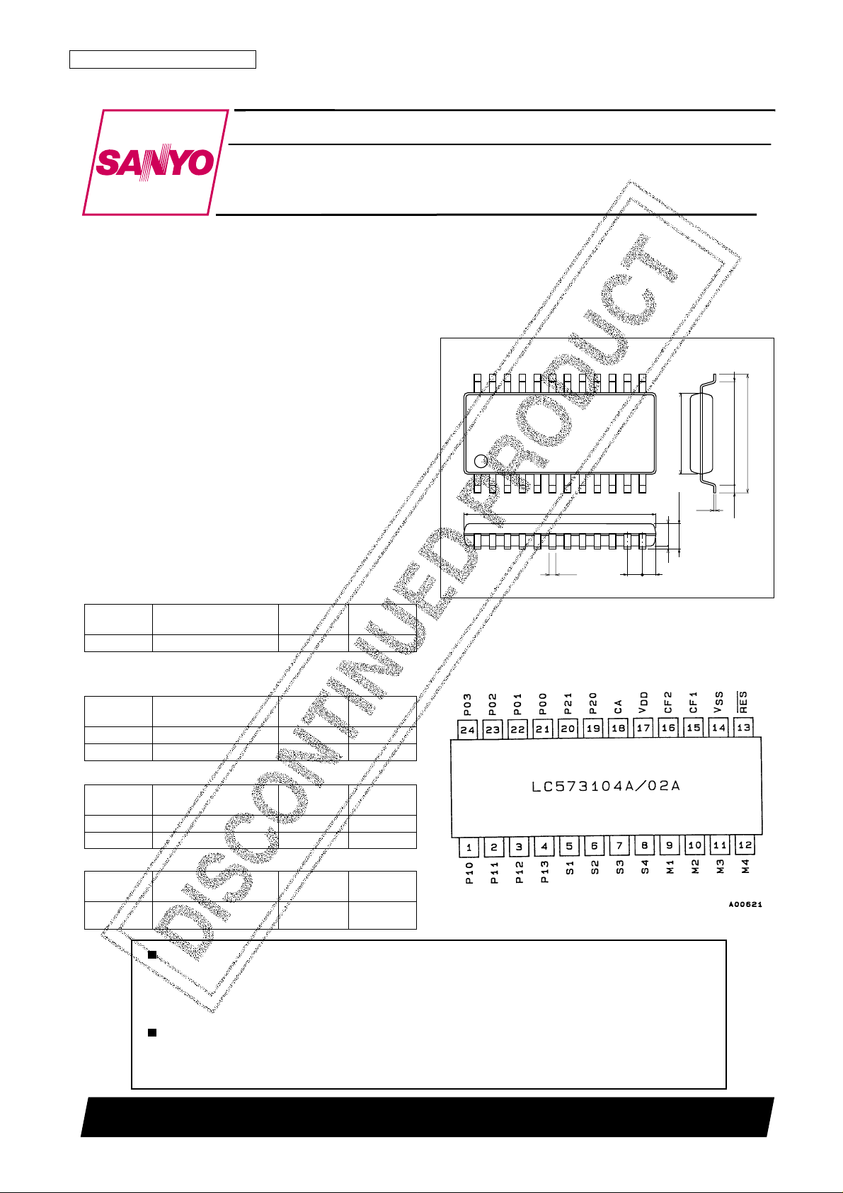
Package Dimensions
unit: mm
3112-MFD24S
Pin Assignment
Preliminary
112
24
13
12.6
0.8
1.0
0.15
0.35
5.4
6.35
7.6
0.625
1.8max
1.5
0.1
SANYO: MFP24S
[LC573010A, 573015A]
Cycle System clock Oscillation Supply
time generator frequency voltage
17.6 µsec Ceramic oscillation circuit 455 kHz 2.3 to 6.0 V
Current System clock Oscillation Supply
drain generator frequency voltage
150 µA typ CR oscillation 455 kHz 3.0 V
400 µA typ CR oscillation 455 kHz 5.0 V
Current System clock Oscillation Supply
drain generator frequency voltage
80 µA typ CR oscillation 455 kHz 3.0 V
300 µA typ CR oscillation 455 kHz 5.0 V
Leakage
Condition
Oscillation Supply
current frequency voltage
0.1 µA typ
When CR oscillation is at
455 kHz 5.0 V
STOP mode
CMOS IC
Ordering number : EN5899
LC573010A, 573015A
4-bit Single Chip Microcontroller
82198RM (OT) No. 5899-1/12
SANYO Electric Co.,Ltd. Semiconductor Bussiness Headquarters
TOKYO OFFICE Tokyo Bldg., 1-10, 1 Chome, Ueno, Taito-ku, TOKYO, 110-8534 JAPAN
Any and all SANYO products described or contained herein do not have specifications that can handle
applications that require extremely high levels of reliability, such as life-support systems, aircraft’s
control systems, or other applications whose failure can be reasonably expected to result in serious
physical and/or material damage. Consult with your SANYO representative nearest you before using
any SANYO products described or contained herein in such applications.
SANYO assumes no responsibility for equipment failures that result from using products at values that
exceed, even momentarily, rated values (such as maximum ratings, operating condition ranges, or other
parameters) listed in products specifications of any and all SANYO products described or contained
herein.
Page 2
• Port
– Input port (S port, M port) : 2-port (8 pins) [Key scan input port]
– Input/Output port : 3-port (10 pins)
P0 port, P1 port 2-port (8 pins) [Key scan output port]
P2 port 1-port (2 pins) [Key scan expansion port]
[LED direct drivable port]
• Infrared remote control carrier generation circuit
– Software-controllable remote control carrier output ON/OFF.
– Software-controllable carrier frequency and duty ratio.
<38 kHz-1/3 duty, 38 kHz-1/2 duty, 57 kHz-1/2 duty>
(When fixed carrier signal is output, it is specified by mask option)
– 1 kHz to 200 kHz infrared remote control transmission carrier frequency.
(When carrier output is selected by timer at mask option, and when 455 kHz CR oscillator is used)
– Infrared carrier output-dedicated terminal built-in (CA terminal).
– 108 ms HALT-mode cancel signal output.
• Timer
– 16-bit software-controllable timer
Timer input clock : Ceramic (CR) oscillation frequency (455 kHz)
– 108 ms HALT release request signal generation timer (Free running timer)
– Watchdog timer (changed over between USED/UNUSED by mask option)
• Sub-routine stack level
– 2 levels
• Oscillation circuit
– Ceramic (CR) oscillation circuit : 455 kHz (for System clock generation), feedback resistor built-in.
• Standby function
– HALT mode
HALT mode used to reduce current drain.
HALT mode suspends program execution.
Following shows how to release the HALT mode.
(A) System reset
(B) HALT mode release request signal
– HOLD mode
HOLD mode stops ceramic resonator (CR). The HOLD mode can be released in two ways.
(A) System reset
(B) Apply H level input to S port pin or M port pin. (However, it is necessary to set S port or M port HOLD mode
release permission flag beforehand.)
• Form of shipment
– MFP-24S (1.0 mm pitch)
Note : When dipping in solder to mount the MFP package on board, contact SANYO for instructions.
No. 5899-2/12
LC573010A, 573015A
Page 3
No. 5899-3/12
LC573010A, 573015A
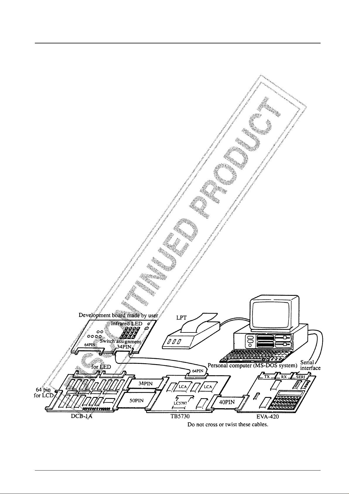
The Application Development System for the LC573100 Series.
Manual
(1) Users Manual : LC573100 Series Users Manual
(2) Development Tool Manual : LC573100 Series Development Tool Manual
Development Tools
• Tools for application development of the LC573100 Series
(1) Personal computer (MS-DOS based)
(2) Cross assembler (LC573100. EXE)
(3) Mask option generator (SU573100. EXE)
• Tools to evaluate application development of the LC573100 Series.
(1) EVA chip (LC5797)
Note : 1 As RAM capacity differs between EVA chip (LC5797) and the LC573100 Series, always check before
programming and debugging.
LC573010A/LC573015S : 64 × 4 bits
LC5797 : 256 × 4 bits
Note : 2 Always keep the DPH value in mind when programming. Only DPH ‘0’ to ‘3’ may be used as the RAM
address.
If DPH other than ‘0’ to ‘3’ is used as RAM address when programming, SANYO will not be liable for any
trouble caused.
(2) EVA chip board (TB5730)
Note : The application evaluation board is the evaluation board made by the user.
(3) Evaluation board [EVA420 (Monitor ROM : ER-573000)]
(4) Display and mask option data control board [DCB-1A (REV3.6)]
Development Support System Outline
Page 4
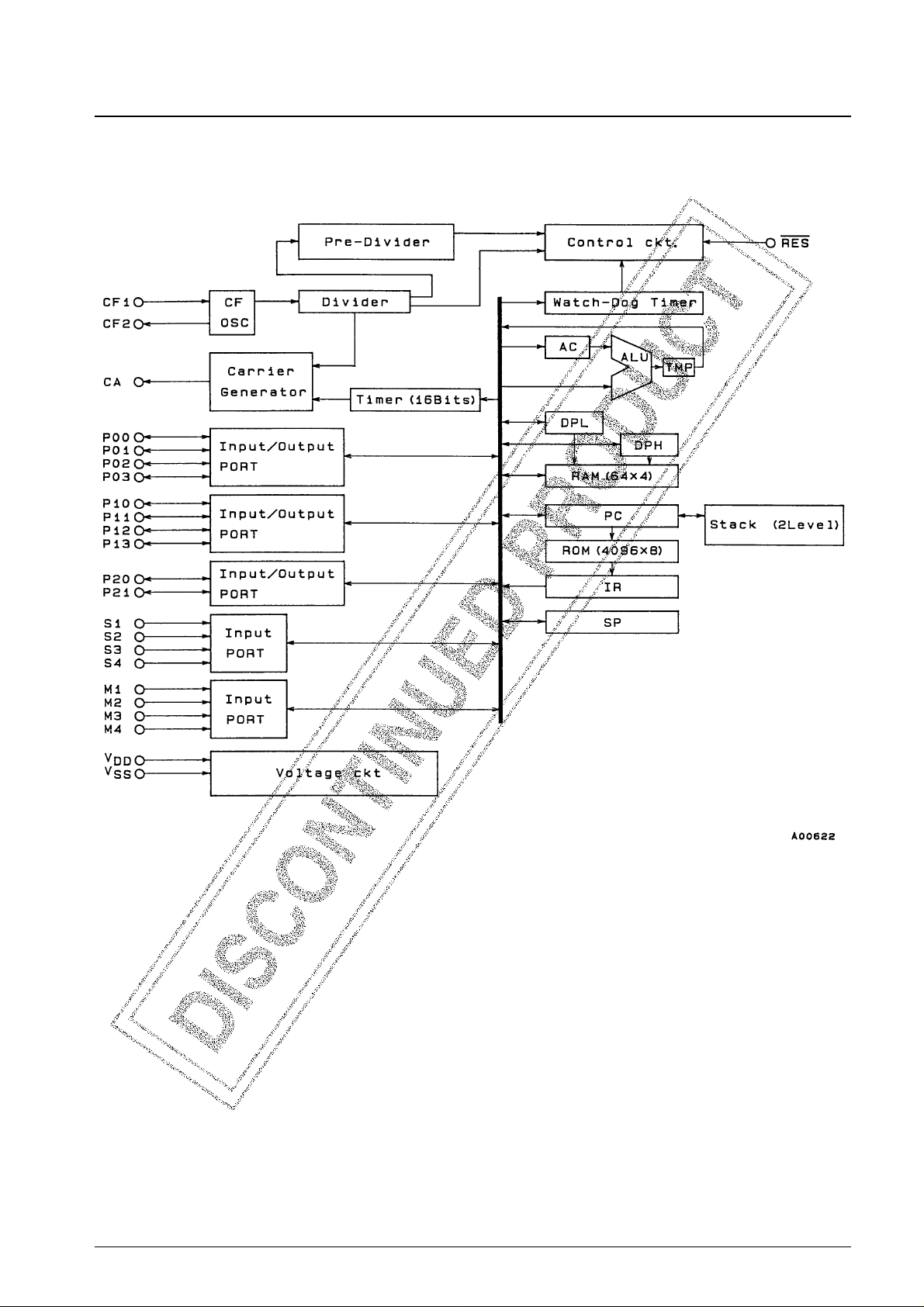
Block Diagram
No. 5899-4/12
LC573010A, 573015A
Page 5

No. 5899-5/12
LC573010A, 573015A
Pin Functions
Pin Assignment
MFP24S Pin Input/
Function description Option Reset status
Pin no. name output
17 V
DD
– Supply voltage. See Figure 1.
14 V
SS
– Ground. See Figure 1.
15 CF1 Input
Used for system clock oscillation
• 455 kHz ceramic resonator is connected between CF1 and CF2 for oscillation.
16 CF2 Output • Stops oscillation when receiving CR oscillation stop command.
5S1
Input port S.
6S2
• LSI system is reset by charging V
DD
to S1 to S4 simultaneously. (Mask option)
7S3
Input • Data is loaded in accumulator.
8S4
9 M1 Input port M.
10 M2
Input
Data loaded in accumulator
11 M3
12 M4
21 P00 Input/output port
22 P01 Input/ • Data loaded in accumulator.
23 P02 output • Output pin to output data from accumulator. (P-ch open drain output)
24 P03
1 P10 Input/output port
2 P11 Input/ • Data loaded in accumulator.
3 P12 output • Output pin to output data from accumulator. (P-ch open drain output)
4P13
Input/output port
19 P20 Input/ • Data loaded in accumulator.
20 P21 output • Output pin to output data from accumulator. (P-ch open drain output)
• LED direct drivable pin
Remote control carrier output.
18 CA Output
13 RES Input Reset input. Internal pull-up resistor.
(1) Low level
HOLD Tr
YES/NO
(2) Reset by S1
to S4.
• Pull-down
resistor ON
• Reset signal
ENABLE
Fixed carrier
output/carrier
output by timer
• At reset low
level
• At fixed carrier
output 38 kHz1/3 duty
Low level HOLD
Tr YES/NO
• Pull-down
resistor ON
Page 6

Supply Connections
Figure 1 Supply Connections
No. 5899-6/12
LC573010A, 573015A
D1 : Infrared LED
D2 : Monitor LED
(max : 8 × 8 64 keys)
←
Page 7

Mask Option
Input port option
No. 5899-7/12
LC573010A, 573015A
Option Circuit Remarks
Next port switches over in
sequence.
• S1 to S4, M1 to M4 Input signal
level Hold Tr selection
• Low level hold Tr used.
• Low level hold Tr not used.
Low level hold
Tr selection
Reset signal option by S port
Option Circuit Remarks
Selects signal for resetting IC
system by simultaneously charging
High level to S1 to S4.
• Allow
• Prohibit
Carrier standard clock generation circuit option for remote control
Option Circuit Remarks
Software-controllable carrier
frequency and duty.
• Following carrier frequency and
duty may be selected by setting
control register 4.
(1) 38 kHz-1/3 duty
(2) 38 kHz-1/2 duty
(3) 57 kHz-1/2 duty
Timer 8-bit overflow signal
generates carrier signal for infrared
remote control.
Fixed 1/2 duty
Resetting IC by
S port
38/57 kHz
Timer 8-bit overflow
Page 8

No. 5899-8/12
LC573010A, 573015A
Watchdog timer circuit option
Option Circuit Remarks
Watchdog timer used/unused
selection
Watchdog timer
selection
Specifications
Absolute Maximum Ratings at Ta = ±25 +2°C, V
SS
= 0 V
Parameter Symbol Conditions Rating Unit
Supply voltage range V
DD
–0.3 to +7.0 V
Input voltage range V
IN
S1 to S4, M1 to M4, RES, P00 to P03, P10 to P13, P20, P21, CF1
–0.3 to V
DD
+0.3 V
(P00 to P03, P10 to P13, P20, P21 are input mode)
Output voltage range V
OUT
CA, P00 to P03, P10 to P13, P20, P21, CF2
–0.3 to V
DD
+0.3 V
(P00 to P03, P10 to P13, P20, P21 are output mode)
I
OUT1
CA (per 1 pin) 25 mA
Output current
I
OUT2
P00 to P03, P10 to P13 (per 1 pin) 500 µA
(Per 1 pin)
I
OUT3
P20, P21 (per 1 pin) 10 mA
I
OUT4
Output pins other than listed above (per 1 pin) 500 µA
Total output current
I
ALL
All pins totalled (except for CA pin) 25 mA
of all pins except CA
Operating temperature
T
opr
–30 to +70 ˚C
range
Storage temperature
T
stg
–40 to +125 ˚C
range
Page 9

No. 5899-9/12
LC573010A, 573015A
Recommended Operating Range at Ta = –30 to +70°C, VSS= 0 V
Figure.2 : CR Oscillation Circuit
Parameter Symbol Conditions
Ratings
Unit
min typ max
Supply voltage V
DD
2.3 6.0 V
Input high level voltage V
IH1
S1 to S4, M1 to M4, P00 to P03, P10 to P13, P20, P21
0.7V
DD
V
DD
V
(P0, P1, P2 ports are input mode)
Input low level voltage V
IL1
V
SS
0.3V
DD
V
Input high level voltage V
IH2
RES
0.75V
DD
V
DD
V
Input low level voltage V
IL2
0 0.25V
DD
V
Operation frequency f
OPG
At CR oscillation, Figure.2 380 455 500 kHz
Page 10

No. 5899-10/12
LC573010A, 573015A
Electrical Characteristics at Ta = –30 to +70°C, VSS= 0 V
Parameter Symbol Conditions
Ratings
Unit
min typ max
R
IN
1A
V
DD
= 2.9 V, VIL= 0.4 V,
150 300 1000 kΩ
S1 to S4, M1 to M4: Low level hold Tr, Figure 3
Input impedance
R
IN
1B
V
DD
= 2.9 V, VIL= 0.4 V, S1 to S4, M1 to M4:
30 50 100 kΩ
Low level pull-down Tr, Figure 3
R
IN
2VDD= 2.9 V, VIH= VDD, RES 10 300 kΩ
Output high level voltage V
OH
1VDD= 2.9 V, IOH= –450 µA, P00 to P03, P10 to P13 VDD–0.45 V
Output off-leak current
|I
OFF
|
V
DD
= 2.9 V, P00 to P03, P10 to P13
V
IN
= V
SS
1.0 µA
|I
OFF
|V
IN
= V
DD
1.0 µA
Output high level voltage V
OH
2VDD= 2.9 V, IOH= –10 mA, P20, P21 VDD–1.5 V
Output off-leak current
|I
OFF
|
VDD= 2.9 V, P20, P21
VIN= V
SS
1.0 µA
|I
OFF
|V
IN
= V
DD
1.0 µA
Output current (H) I
OH
1VDD= 3.0 V, VOH= VDD–1.5 V, CA –12 –6mA
Output current (L) I
OL
1VDD= 3.0 V, VOH= 0.9 V, CA 2 5 mA
HALT-mode supply
IDD1
V
DD
= 3.0 V, 455 kHZ CR oscillation, Ccd = Ccg = 150 pF,
80 300 µA
current Ta≤ 50˚C, Figure 5
Operating Current I
DD
2
V
DD
= 3.0 V, 455 kHz CR oscillation, Ccd = Ccg = 150 pF,
150 500 µA
Ta ≤ 50˚C, Figure 5
Supply leak current 1 I
LEAK
1
V
DD
= 3.0 V
Ta = 25˚C 0.2 1 µA
Supply leak current 2 I
LEAK
2 Ta = 50˚C15µA
Oscillator start-up
V
ST
2.3 V
voltage
Ccd = Ccg = 150 pF, 455 kHz CR oscillation, Figure 4
Oscillator sustaining
V
SUS
2.0 V
voltage
Oscillator start-up time t
ST
VDD= 2.3 V, Ccd = Ccg = 150 pF, 455 kHz CR oscillation, Figure 4 30 ms
Recommended Oscillators
Oscillator Manufacturer Part number Ccg Ccd
455 kHz ceramic
Kyocera KRB-455BK/Y 150 pF 150 pF
oscillator
Murata CSB455E 150 pF 150 pF
Fuji Ceramics POE-455 150 pF 150 pF
Page 11

No. 5899-11/12
LC573010A, 573015A
Electrical Characteristics at Ta = –30 to +70°C, VSS= 0 V
Parameter Symbol Condition
Ratings
Unit
min typ max
R
IN
1A
V
DD
= 5.0 V, VIL= 0.4 V, S1 to S4, M1 to M4: Low level hold
70 200 300 kΩ
Input impedance
Tr, Figure 3
R
IN
1B VDD= 5.0 V, S1 to S4, M1 to M4: Low level pull-down Tr, Figure 3 30 50 100 kΩ
R
IN
2VDD= 5.0 V, RES 10 300 kΩ
Output high level
V
OH
1VDD= 5.0 V, IOH= –750 µA, P00 to P03, P10 to P13 VDD–0.75 V
voltage
Output off-leak current
|I
OFF
|
VDD= 5.0 V, P00 to P03, P10 to P13
VIN= V
SS
1.0 µA
|I
OFF
|V
IN
= V
DD
1.0 µA
Output high level
V
OH
2VDD= 5.0 V, IOH= –10 mA, P20, P21 VDD–0.5 V
voltage
Output off-leak current
|I
OFF
|
V
DD
= 5.0 V, P20, P21
V
IN
= V
SS
1.0 µA
|I
OFF
|V
IN
= V
DD
1.0 µA
Output current (H) I
OH
1VDD= 5.0 V, VOH= V
DD
– 2.5 V, CA 10 20 mA
Output current (L) I
OL
1VDD= 5.0 V, VOL= 0.9 V, CA 2 mA
HALT-mode supply
I
DD
1
V
DD
= 5.0 V, 455 kHz CR oscillation, Ccd = Ccg = 150 pF,
300 400 µA
current Ta ≤ 50˚C, Figure 5
Operating current I
DD
2
V
DD
= 5.0 V, 455 kHz CR oscillation Ccd = Ccg = 150 pF,
400 500 µA
Ta ≤ 50˚C, Figure 5
Supply leak current 1 I
LEAK
1
V
DD
= 5.0 V
Ta = 25˚C 0.2 1 µA
Supply leak current 2 I
LEAK
2 Ta = 50˚C15µA
Oscillator start-up
V
ST
2.3 V
voltage
Ccd = Ccg = 150 pF, 455 kHz CR oscillation, Figure 4
Oscillator sustaining
V
SUS
2.0 V
voltage
Oscillator start-up time t
ST
VDD= 2.3 V, Ccd = Ccg = 150 pF, 455 kHz CR oscillation, Figure 4 30 ms
Figure 3 : S1 to S4, M1 to M4 Input Structure
Figure 5 : Supply Current Measuring Circuit
Figure4 : Oscillator Start-Up Voltage, Oscillator
Sustaining Voltage, and Oscillator Start-Up
Time Measuring Circuit
Note :CR is 455 kHz, S-PORT: M-PORT: Input Pull-down transistor is on. RES
terminal has resistor built-in and is open. I/O-port is set at output mode and
data is high.
‘L’ level pull-down Tr
‘L’ level Hold Tr
Charged by program
Page 12

PS No. 5899-12/12
LC573010A, 573015A
This catalog provides information as of December, 1998. Specifications and information herein are
subject to change without notice.
Specifications of any and all SANYO products described or contained herein stipulate the performance,
characteristics, and functions of the described products in the independent state, and are not guarantees
of the performance, characteristics, and functions of the described products as mounted in the customer’s
products or equipment. To verify symptoms and states that cannot be evaluated in an independent device,
the customer should always evaluate and test devices mounted in the customer’s products or equipment.
SANYO Electric Co., Ltd. strives to supply high-quality high-reliability products. However, any and all
semiconductor products fail with some probability. It is possible that these probabilistic failures could
give rise to accidents or events that could endanger human lives, that could give rise to smoke or fire,
or that could cause damage to other property. When designing equipment, adopt safety measures so
that these kinds of accidents or events cannot occur. Such measures include but are not limited to protective
circuits and error prevention circuits for safe design, redundant design, and structural design.
In the event that any or all SANYO products (including technical data, services) described or contained
herein are controlled under any of applicable local export control laws and regulations, such products must
not be exported without obtaining the export license from the authorities concerned in accordance with the
above law.
No part of this publication may be reproduced or transmitted in any form or by any means, electronic or
mechanical, including photocopying and recording, or any information storage or retrieval system,
or otherwise, without the prior written permission of SANYO Electric Co., Ltd.
Any and all information described or contained herein are subject to change without notice due to
product/technology improvement, etc. When designing equipment, refer to the “Delivery Specification”
for the SANYO product that you intend to use.
Information (including circuit diagrams and circuit parameters) herein is for example only; it is not
guaranteed for volume production. SANYO believes information herein is accurate and reliable, but
no guarantees are made or implied regarding its use or any infringements of intellectual property rights
or other rights of third parties.
 Loading...