

Page 1
Ordering number : ENN*6477
51200RM (OT) No. 6477-1/12
Overview
The LC4132C is a segment driver for large-scale dot
matrix LCDs. The LC4132C latches 240 bits of display
data sent from the controller (in 4- or 8-bit parallel units)
and generates the LCD drive signals. The LC4132C and
the LC4102C common driver form a chip set that can
drive a large-screen LCD panel.
Features
• CMOS (p-substrate) high voltage process
• LCD drive voltage: 36 V
• Logic system supply voltage: 2.7 to 5.5 V
• fcp max: 12 MHz (VDD= 5 V ±10%), 10 MHz (VDD=
2.7 to 4.5 V)
• Slim chip
• Can be switched between 4-bit an 8-bit parallel input.
• Output direction switching
• Display off function that holds the LCD drive voltages
at fixed levels.
• Display duty: 1/160 to 1/480
• Supports COG (chip on glass) mounting. (Gold bump
pads are used.)
LC4132C
SANYO Electric Co.,Ltd. Semiconductor Company
TOKYO OFFICE Tokyo Bldg., 1-10, 1 Chome, Ueno, Taito-ku, TOKYO, 110-8534 JAPAN
Dot Matrix STN LCD Segment Driver
CMOS IC
Any and all SANYO products described or contained herein do not have specifications that can handle
applications that require extremely high levels of reliability, such as life-support systems, aircraft’s
control systems, or other applications whose failure can be reasonably expected to result in serious
physical and/or material damage. Consult with your SANYO representative nearest you before using
any SANYO products described or contained herein in such applications.
SANYO assumes no responsibility for equipment failures that result from using products at values that
exceed, even momentarily, rated values (such as maximum ratings, operating condition ranges, or other
parameters) listed in products specifications of any and all SANYO products described or contained
herein.
Page 2
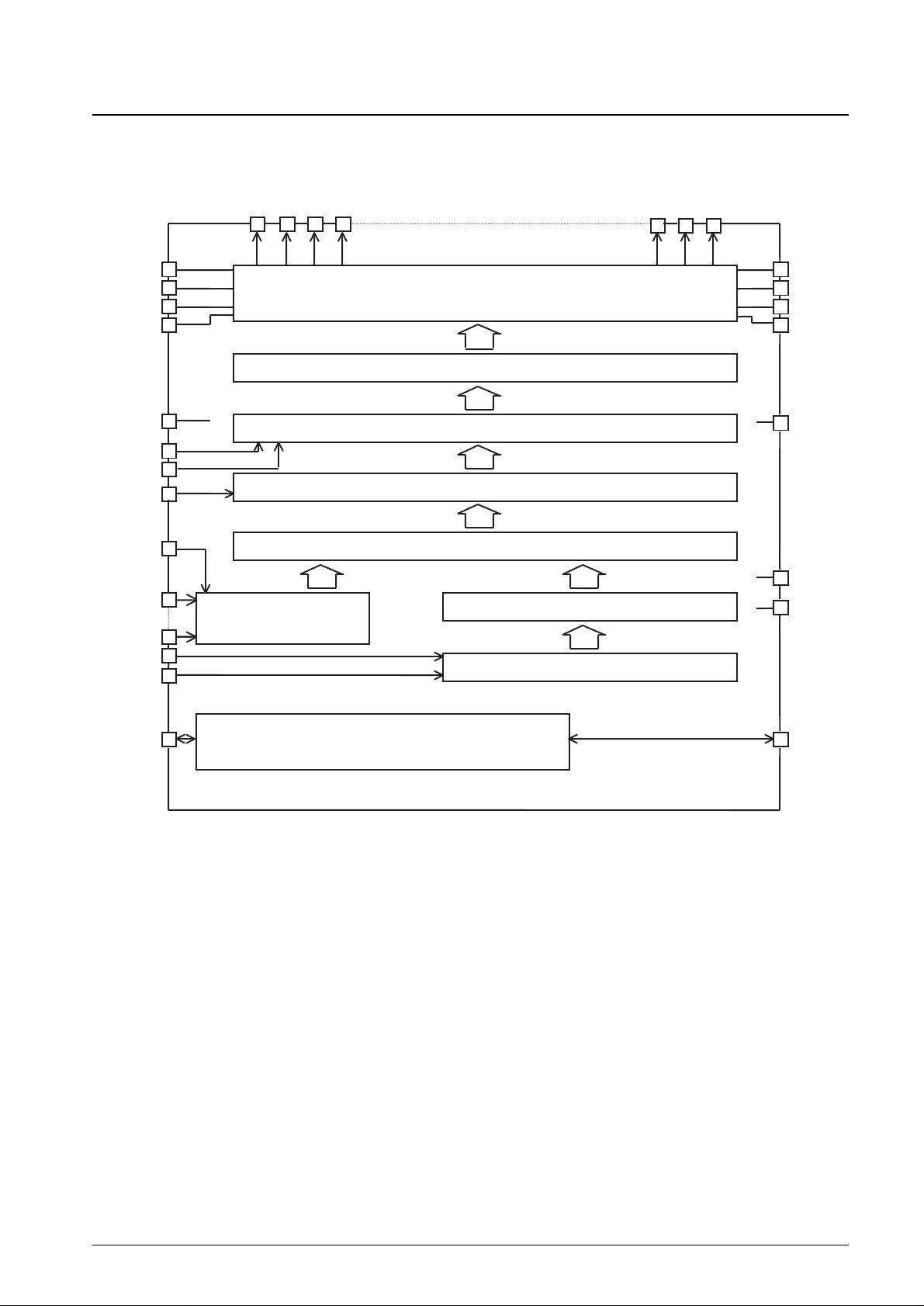
Block Diagram
No. 6477-2/12
LC4132C
O1
V0
V0
4 Level LCD Drive Circuit (240 bits)
Output Control
Level Shifter
2nd Latch (240 bits)
Bits Control
Address Decoder
Address Counter
Chip Disable & Latch Control
1st Latch (8 bits × 30)
V2
V3
V5
VDDH
VDD
VSS
EIO2
V2
V3
V5
VDDH
DISP
M
LOAD
BS
D0
to
D7
CP
R/L
EIO1
O2
O3
O4
O238
O239
O240
Page 3
No. 6477-3/12
LC4132C
The electrical characteristics listed below apply when packaged in the Sanyo PGA-208 package.
Notes: 1. D0 to D7, LOAD, CP, R/L, DISP, M, EIO1, EIO2, BS
2. The following relationships must hold for V0, V2, V3, and V5: V
DDH
≥ V0 ≥ V2 ≥ V
DDH
– 7 V, and 7 V ≥ V3 ≥ V5 ≥ VSS.
Notes: 3. D0 to D7, LOAD, CP, R/L, M, DISP, BS, EIO1, EIO2
4. The following relationships must hold for V0, V2, V3, and V5: V
DDH
≥ V0 ≥ V2 ≥ V
DDH
– 7 V, and 7 V ≥ V3 ≥ V5 ≥ VSS.
At power on: The logic system power supply must be applied before the high-voltage system power supply. (Or they must both be applied at the
same time.)
At power off: The high-voltage system power supply must be turned off before the logic system power supply. (Or they must both be turned off at
the same time.)
Note: 5. The clock rise time (tr) and the clock fall time (tf) must meet the conditions (1) and (2) shown below.
1
—— – tw (cph) – tw (cpl)
fcp
(1) tr, tf < ———————————— (2) tr, tf ≤ 50 ns
2
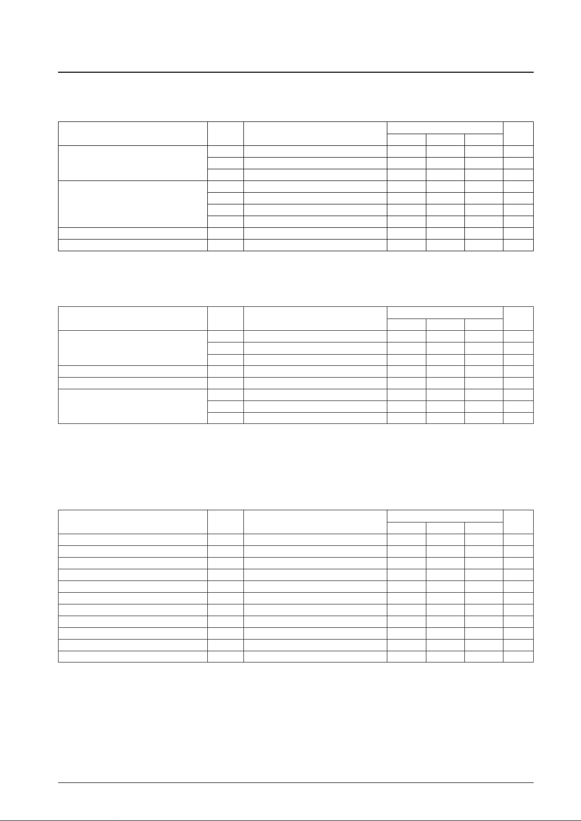
Parameter Symbol Conditions
Ratings
Unit
min typ max
V
DD
max V
DD
–0.3 7.0 V
Maximum supply voltage V
DDH
max V
DDH
–0.3 40.0 V
V
SS
max V
SS
–0.3 0.3 V
V
IN
*
1
–0.3 VDD+ 0.3 V
Input voltage
V0, V2 V0, V2 *
2
V
DDH
– 7.0 V
DDH
+ 0.3 V
V3 V3 *
2
–0.3 VSS+ 7.0 V
V5 V5 *
2
–0.3 0.3 V
Operating temperature Topr –20 +75 °C
Storage temperature Tstg –55 +125 °C
Absolute Maximum Ratings at VSS= 0 V
Parameter Symbol Conditions
Ratings
Unit
min typ max
V
DDVDD
2.7 5.5 V
Supply voltage V
DDHVDDH
20 36 V
V
SS
V
SS
0 V
Input high-level voltage V
IH
*
3
0.8 V
DD
V
DD
V
Input low-level voltage V
IL
*
3
0 0.2 V
DD
V
V0, V2 V0, V2 *
4
V
DDH
– 7.0 V
DDH
V
Input voltage V3 V3 *
4
0 V
SSH
+ 7.0 V
V5 V5 *
1
0 V
Allowable Operating Ranges at Ta = –20 to +75°C, VSS= 0 V
Parameter Symbol Conditions
Ratings
Unit
min typ max
CP clock frequency fcp CP 12 MHz
High-level load pulse width tw (ldH) LOAD 50 ns
High-level clock pulse width tw (cpH) CP 20 ns
Low-level clock pulse width tw (cpL) CP 20 ns
LOAD/CP setup time tsu (ld) LOAD, CP 100 ns
LOAD/CP hold time tho (ld) LOAD, CP 200 ns
DATA/CP setup time tsu (cp) CP, D0 to D7 10 ns
DATA/CP hold time tho (cp) CP, D0 to D7 10 ns
EIO input setup time tsu (ei) CP, EIO1, EIO2 24 ns
Clock rise time tr LOAD, CP *
5
50 ns
Clock fall time tf LOAD, CP *
5
50 ns
VDD= 5 V ±10%, Ta = –20 to +75°C, VSS= 0 V
Page 4
No. 6477-4/12
LC4132C
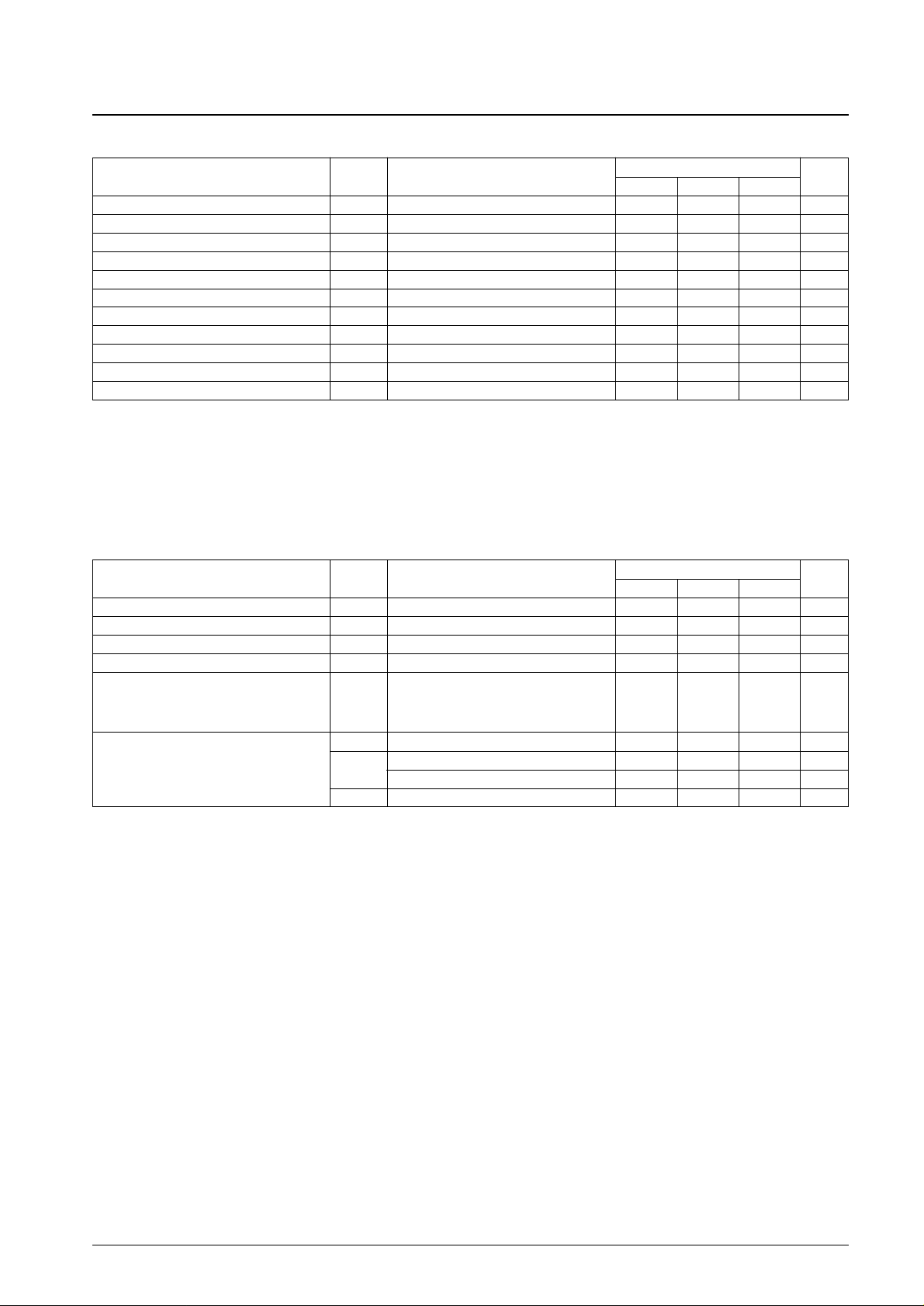
Note: 6. The clock rise time (tr) and the clock fall time (tf) must meet the conditions (1) and (2) shown below.
1
—— – tw (cph) – tw (cpl)
fcp
(1) tr, tf < ———————————— (2) tr, tf ≤ 50 ns
2
Parameter Symbol Conditions
Ratings
Unit
min typ max
CP clock frequency fcp CP 10 MHz
High-level load pulse width tw (ldH) LOAD 50 ns
High-level clock pulse width tw (cpH) CP 37 ns
Low-level clock pulse width tw (cpL) CP 37 ns
LOAD/CP setup time tsu (ld) LOAD, CP 100 ns
LOAD/CP hold time tho (ld) LOAD, CP 350 ns
DATA/CP setup time tsu (cp) CP, D0 to D7 35 ns
DATA/CP hold time tho (cp) CP, D0 to D7 35 ns
EIO input setup time tsu (ei) CP, EIO1, EIO2 30 ns
Clock rise time tr LOAD, CP *
6
50 ns
Clock fall time tf LOAD, CP *
6
50 ns
VDD= 2.7 to 4.5 V, Ta = –20 to +75°C, VSS= 0 V
Notes: 7. D0 to D7, LOAD, CP, R/L, M, DISP, EIO1, 2, BS
8. V
O
is the voltage applied by an on-state output, V0 = V
DDH
, V2 = 18/20 (V
DDH
– VSS), V3 = 2/20 (V
DDH
– VSS), V5 = VSS.
9. Measured when either LOAD = 28 kHz, CP = 10 MHz, and M = 75 Hz, or with no load and input at V
IH
= VDDor VIL= VSS.
10. The current drain in standby mode. Or when EIOn (input) = V
DD
.
Parameter Symbol Conditions
Ratings
Unit
min typ max
Input high-level voltage I
IH
VIN= VDD*
7
5 µA
Input low-level voltage I
IL
1 VIN= VSS*
7
–5 µA
Output high-level voltage V
OHIO
= –0.4 mA: EIO1, EIO2 VDD– 0.4 V
DD
V
Output low-level voltage V
OLIO
= 0.4 mA: EIO1, EIO2 V
SS
0.4 V
V
DDH
= 36 V *
8
Output on resistance R
OUT
V0 – VO= 0.5 V, V2 – VO= 0.5 V
1 3 kΩ
V
O
– V3 = 0.5 V, VO– V5 = 0.5 V
: O1 to O240
I
DD
VDD= 2.7 to 5.5 V 5.0 mA
Current drain I
DDH
VDD= 2.7 to 5.5 V, V
DDH
= 32 V *
9
3.0 mA
V
DD
= 5 V ±10%, V
DDH
= 36 V 3.0 mA
I
ST
*
10
500 µA
Electrical Characteristics at Ta = –20 to +75°C, VDD= 2.7 to 5.5 V, VSS= 0 V
Page 5

No. 6477-5/12
LC4132C
Parameter Symbol Conditions
Ratings
Unit
min typ max
EIO output delay time td (eo) 30 pF capacitance load: CP, EIO1, EIO2 40 ns
LOAD/EIO output delay time td (leo) 30 pF capacitance load: LOAD, EIO1, EIO2 70 ns
LOAD/On delay time td (ldo) 100 pF capacitance load: LOAD, O1 to O240 700 ns
M/On delay time td (mo) 100 pF capacitance load: M, O1 to O240 700 ns
Switching Characteristics at Ta = –20 to +75°C, VSS= 0 V
Parameter Symbol Conditions
Ratings
Unit
min typ max
EIO output delay time td (eo) 30 pF capacitance load: CP, EIO1, EIO2 80 ns
LOAD/EIO output delay time td (leo) 30 pF capacitance load: LOAD, EIO1, EIO2 130 ns
LOAD/On delay time td (ldo) 100 pF capacitance load: LOAD, O1 to O240 3 µs
M/On delay time td (mo) 100 pF capacitance load: M, O1 to O240 3 µs
VDD= 2.5 to 4.5 V
Timing Chart (VIH= 0.8 VDD, VIL= 0.2 VDD)
0.2VDD
0.8VDD
tr(ld)
tw(ldH)
tf(ld)
tho(ld)
tsu(ld)
td(mo)
tsu(cp)
tho(cp)
td(leo)
tr(cp)
tw(cpH)
tf(cp)
tw(cpL)
td(eo)
tsu(ei)
td(ldo)
EIOn (output)
(input to the next stage)
VDD= 5 V ±10%
LOAD
CP
D0 to D7
M
On
Page 6

No. 6477-6/12
LC4132C
Pin Functions
Pin I/O Function
LCD drive outputs
O1 to O240 O
V0 level drive voltage application (selected level)
V2 level drive voltage application (unselected level)
V3 level drive voltage application (unselected level)
V5 level drive voltage application (selected level)
V0
V2
V3
V5
I
I
I
I
M Data DISP On
H H H V0
H L H V2
L L H V3
L H H V5
* * L V5
R/L EIO1 EIO2
L IN OUT
H OUT IN
R/L BS O1 to O240 outputs
O1 O2 O3 O4 → ... O237 O238 O239 O240
L ↑ ↑ ↑ ↑ ↑ ↑ ↑ ↑
H
D7 D6 D5 D4 D3 D2 D1 D0
O1 O2 O3 O4 → ... O237 O238 O239 O240
H ↑ ↑ ↑ ↑ ↑ ↑ ↑ ↑
D0 D1 D2 D3 D4 D5 D6 D7
O1 O2 O3 O4 → ... O237 O238 O239 O240
L ↑ ↑ ↑ ↑ ↑ ↑ ↑ ↑
L
D3 D2 D1 D0 D3 D2 D1 D0
O1 O2 O3 O4 → ... O237 O238 O239 O240
H ↑ ↑ ↑ ↑ ↑ ↑ ↑ ↑
D0 D1 D2 D3 D0 D1 D2 D3
High-voltage system power supply
V
DDH
—
Logic system power supply
V
DD
—
GND
V
SS
—
LCD off function. When this pin is low, all outputs are held at the V5 level.DISP I
Alternation signal inputM I
Enable I/O
Enable input: The enable input at the initial stage is fixed at the V
SS
level, and the enable inputs of later stages are connected to
the enable output from the previous stage.
Enable output: When cascade connection is used, the enable output is connected to the enable input of the next stage.
EIO1
EIO2
I/O
I/O
Data acquisition clock (falling edge)CP I
Data load clock (falling edge)LOAD I
Data shift direction setting
R/L I
Parallel data inputs
D0 to D7
I
Input bus width setting. A high level selects 8-bit input, and a low level selects 4-bit input. In 4-bit input mode, D0 to D3 are used
for data acquisition and D4 to D7 must be tied to ground.
BS
I
* don't care
Page 7

Pad Assignment
No. 6477-7/12
LC4132C
NC
O5
O6
O7
O8
O233
NC
V5
NC
V5
V5
V3
V3
V3
V2
V2
V2
V0
V0
V0
VDDH
VDDH
VDDH
VSS
VSS
VSS
VDD
VDD
VDD
VDD
VDD
VDD
VDD
VSS
VSS
VSS
VSS
VSS
VSS
VSS
BS
BS
R/L
R/L
NC
NC
DISP
DISP
M
M
LOAD
CP
CP
EIO1
LOAD
EIO1
EIO2
EIO2
VSS
VSS
VSS
VDD
VDD
VDD
D7
D7
D6
D6
D5
D5
D4
D4
D3
D3
D2
D2
D1
D1
D0
D0
VDD
VDD
VDD
VSS
VSS
VSS
VSS
VSS
VSS
VSS
VDDH
VDDH
VDDH
V0
V0
V0
V2
V2
V2
V3
V3
V3
V5
V5
V5
NC
NCNCNCNCNCNCO1O2O3
O4
O234
O235
O236
NC
NCNCNCNCNCNCNC
O240
O239
O238
O237
Origin (0, 0)
Chip size: 15.7 × 2.0 mm
Y (+)
X (+)
Page 8
No. 6477-8/12
LC4132C
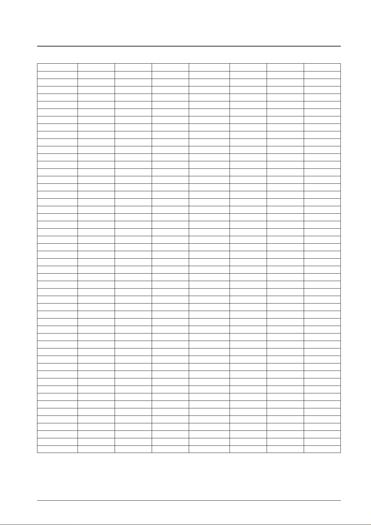
LC4132C Pad Coordinates
Pin X coordinate Y coordinate Bump type Pin X coordinate Y coordinate Bump type
NC –7687.0 –794.0 D V
SS
–172.0 –806.0 A
V5 –7587.0 –794.0 A V
SS
7.0 –806.0 A
V5 –7487.0 –794.0 A V
SS
186.0 –806.0 A
V5 –7387.0 –794.0 A V
DD
365.0 –806.0 A
V3 –7287.0 –794.0 A V
DD
544.0 –806.0 A
V3 –7187.0 –794.0 A V
DD
723.0 –806.0 A
V3 –7087.0 –794.0 A D7 949.0 –806.0 A
V2 –6987.0 –794.0 A D7 1174.0 –806.0 A
V2 –6887.0 –794.0 A D6 1399.0 –806.0 A
V2 –6787.0 –794.0 A D6 1624.0 –806.0 A
V0 –6687.0 –794.0 A D5 1849.0 –806.0 A
V0 –6587.0 –794.0 A D5 2074.0 –806.0 A
V0 –6487.0 –794.0 A D4 2299.0 –806.0 A
V
DDH
–6387.0 –794.0 A D4 2524.0 –806.0 A
V
DDH
–6287.0 –794.0 A D3 2749.0 –806.0 A
V
DDH
–6187.0 –794.0 A D3 2974.0 –806.0 A
V
SS
–6087.0 –794.0 A D2 3199.0 –806.0 A
V
SS
–5987.0 –794.0 A D2 3424.0 –806.0 A
V
SS
–5887.0 –794.0 A D1 3649.0 –806.0 A
V
DD
–5787.0 –794.0 A D1 3874.0 –806.0 A
V
DD
–5687.0 –794.0 A D0 4099.0 –806.0 A
V
DD
–5587.0 –794.0 A D0 4324.0 –806.0 A
V
DD
–5487.0 –794.0 A V
DD
4446.2 –794.0 A
V
DD
–5387.0 –794.0 A V
DD
4646.2 –749.0 A
V
DD
–5287.0 –794.0 A V
DD
4846.2 –794.0 A
V
DD
–5187.0 –794.0 A V
SS
5046.2 –794.0 A
V
SS
–5087.0 –794.0 A V
SS
5246.2 –794.0 A
V
SS
–4987.0 –794.0 A V
SS
5446.2 –794.0 A
V
SS
–4887.0 –794.0 A V
SS
5646.2 –794.0 A
V
SS
–4787.0 –794.0 A V
SS
5887.0 –794.0 A
V
SS
–4687.0 –794.0 A V
SS
5987.0 –794.0 A
V
SS
–4587.0 –794.0 A V
SS
6087.0 –794.0 A
V
SS
–4487.0 –794.0 A V
DDH
6187.0 –794.0 A
BS –4161.3 –806.0 A V
DDH
6287.0 –794.0 A
BS –3936.4 –806.0 A V
DDH
6387.0 –794.0 A
R/L –3711.3 –806.0 A V0 6487.0 –794.0 A
R/L –3486.4 –806.0 A V0 6587.0 –794.0 A
NC –3261.3 –806.0 A V0 6687.0 –794.0 A
NC –3036.4 –806.0 A V2 6787.0 –794.0 A
DISP –2811.3 –806.0 A V2 6887.0 –794.0 A
DISP –2586.4 –806.0 A V2 6987.0 –794.0 A
M –2361.3 –806.0 A V3 7087.0 –794.0 A
M –2136.4 –806.0 A V3 7187.0 –794.0 A
LOAD –1911.3 –806.0 A V3 7287.0 –794.0 A
LOAD –1686.4 –806.0 A V5 7387.0 –794.0 A
CP –1461.3 –806.0 A V5 7487.0 –794.0 A
CP –1236.4 –806.0 A V5 7587.0 –794.0 A
EIO1 –1011.3 –806.0 A NC 7687.0 –794.0 D
EIO1 –786.4 –806.0 A
EIO2 –561.3 –806.0 A
EIO2 –336.4 –806.0 A
Continued on next page.
Page 9

No. 6477-9/12
LC4132C
Continued from preceding page.
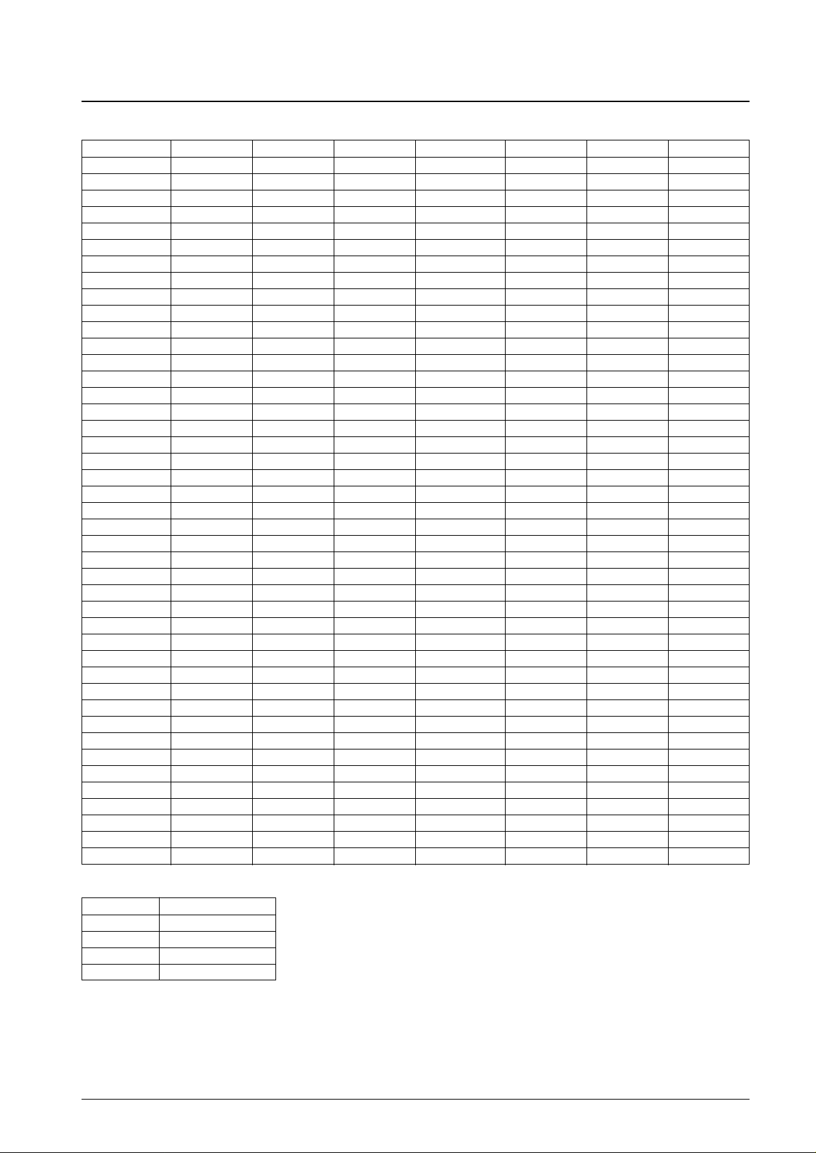
Pin X coordinate Y coordinate Bump type Pin X coordinate Y coordinate Bump type
NC –7676.0 –666.0 B O36 –5577.0 829.0 C
NC –7676.0 –534.0 B O37 –5511.0 829.0 C
NC –7676.0 –402.0 B O38 –5445.0 829.0 C
NC –7676.0 –270.0 B O39 –5379.0 829.0 C
NC –7676.0 –138.0 B O40 –5313.0 829.0 C
NC –7676.0 –6.0 B O41 –5247.0 829.0 C
NC –7676.0 126.0 B O42 –5181.0 829.0 C
O1 –7676.0 258.0 B O43 –5115.0 829.0 C
O2 –7676.0 390.0 B O44 –5049.0 829.0 C
O3 –7676.0 522.0 B O45 –4983.0 829.0 C
O4 –7676.0 654.0 B O46 –4917.0 829.0 C
NC –7689.0 829.0 C O47 –4851.0 829.0 C
O5 –7623.0 829.0 C O48 –4785.0 829.0 C
O6 –7557.0 829.0 C O49 –4719.0 829.0 C
O7 –7491.0 829.0 C O50 –4653.0 829.0 C
O8 –7425.0 829.0 C O51 –4587.0 829.0 C
O9 –7359.0 829.0 C O52 –4521.0 829.0 C
O10 –7293.0 829.0 C O53 –4455.0 829.0 C
O11 –7227.0 829.0 C O54 –4389.0 829.0 C
O12 –7161.0 829.0 C O55 –4323.0 829.0 C
O13 –7095.0 829.0 C O56 –4257.0 829.0 C
O14 –7029.0 829.0 C O57 –4191.0 829.0 C
O15 –6963.0 829.0 C O58 –4125.0 829.0 C
O16 –6897.0 829.0 C O59 –4059.0 829.0 C
O17 –6831.0 829.0 C O60 –3993.0 829.0 C
O18 –6765.0 829.0 C O61 –3927.0 829.0 C
O19 –6699.0 829.0 C O62 –3861.0 829.0 C
O20 –6633.0 829.0 C O63 –3795.0 829.0 C
O21 –6567.0 829.0 C O64 –3729.0 829.0 C
O22 –6501.0 829.0 C O65 –3663.0 829.0 C
O23 –6435.0 829.0 C O66 –3597.0 829.0 C
O24 –6369.0 829.0 C O67 –3531.0 829.0 C
O25 –6303.0 829.0 C O68 –3465.0 829.0 C
O26 –6237.0 829.0 C O69 –3399.0 829.0 C
O27 –6171.0 829.0 C O70 –3333.0 829.0 C
O28 –6105.0 829.0 C O71 –3267.0 829.0 C
O29 –6039.0 829.0 C O72 –3201.0 829.0 C
O30 –5973.0 829.0 C O73 –3135.0 829.0 C
O31 –5907.0 829.0 C O74 –3069.0 829.0 C
O32 –5841.0 829.0 C O75 –3003.0 829.0 C
O33 –5775.0 829.0 C O76 –2937.0 829.0 C
O34 –5709.0 829.0 C O77 –2871.0 829.0 C
O35 –5643.0 829.0 C O78 –2805.0 829.0 C
Continued on next page.
Page 10

No. 6477-10/12
LC4132C
Continued from preceding page.
Pin X coordinate Y coordinate Bump type Pin X coordinate Y coordinate Bump type
O79 –2739.0 829.0 C O122 99.0 829.0 C
O80 –2673.0 829.0 C O123 165.0 829.0 C
O81 –2607.0 829.0 C O124 231.0 829.0 C
O82 –2541.0 829.0 C O125 297.0 829.0 C
O83 –2475.0 829.0 C O126 363.0 829.0 C
O84 –2409.0 829.0 C O127 429.0 829.0 C
O85 –2343.0 829.0 C O128 495.0 829.0 C
O86 –2277.0 829.0 C O129 561.0 829.0 C
O87 –2211.0 829.0 C O130 627.0 829.0 C
O88 –2145.0 829.0 C O131 693.0 829.0 C
O89 –2079.0 829.0 C O132 759.0 829.0 C
O90 –2013.0 829.0 C O133 825.0 829.0 C
O91 –1947.0 829.0 C O134 891.0 829.0 C
O92 –1881.0 829.0 C O135 957.0 829.0 C
O93 –1815.0 829.0 C O136 1023.0 829.0 C
O94 –1749.0 829.0 C O137 1089.0 829.0 C
O95 –1683.0 829.0 C O138 1155.0 829.0 C
O96 –1617.0 829.0 C O139 1221.0 829.0 C
O97 –1551.0 829.0 C O140 1287.0 829.0 C
O98 –1485.0 829.0 C O141 1353.0 829.0 C
O99 –1419.0 829.0 C O142 1419.0 829.0 C
O100 –1353.0 829.0 C O143 1485.0 829.0 C
O101 –1287.0 829.0 C O144 1551.0 829.0 C
O102 –1221.0 829.0 C O145 1617.0 829.0 C
O103 –1155.0 829.0 C O146 1683.0 829.0 C
O104 –1089.0 829.0 C O147 1749.0 829.0 C
O105 –1023.0 829.0 C O148 1815.0 829.0 C
O106 –957.0 829.0 C O149 1881.0 829.0 C
O107 –891.0 829.0 C O150 1947.0 829.0 C
O108 –825.0 829.0 C O151 2013.0 829.0 C
O109 –759.0 829.0 C O152 2079.0 829.0 C
O110 –693.0 829.0 C O153 2145.0 829.0 C
O111 –627.0 829.0 C O154 2211.0 829.0 C
O112 –561.0 829.0 C O155 2277.0 829.0 C
O113 –495.0 829.0 C O156 2343.0 829.0 C
O114 –429.0 829.0 C O157 2409.0 829.0 C
O115 –363.0 829.0 C O158 2475.0 829.0 C
O116 –297.0 829.0 C O159 2541.0 829.0 C
O117 –231.0 829.0 C O160 2607.0 829.0 C
O118 –165.0 829.0 C O161 2673.0 829.0 C
O119 –99.0 829.0 C O162 2739.0 829.0 C
O120 –33.0 829.0 C O163 2805.0 829.0 C
O121 33.0 829.0 C O164 2871.0 829.0 C
Continued on next page.
Page 11
No. 6477-11/12
LC4132C
Continued from preceding page.
Pin X coordinate Y coordinate Bump type Pin X coordinate Y coordinate Bump type
O165 2937.0 829.0 C O208 5775.0 829.0 C
O166 3003.0 829.0 C O209 5841.0 829.0 C
O167 3069.0 829.0 C O210 5907.0 829.0 C
O168 3135.0 829.0 C O211 5973.0 829.0 C
O169 3201.0 829.0 C O212 6039.0 829.0 C
O170 3267.0 829.0 C O213 6105.0 829.0 C
O171 3333.0 829.0 C O214 6171.0 829.0 C
O172 3399.0 829.0 C O215 6237.0 829.0 C
O173 3465.0 829.0 C O216 6303.0 829.0 C
O174 3531.0 829.0 C O217 6369.0 829.0 C
O175 3597.0 829.0 C O218 6435.0 829.0 C
O176 3663.0 829.0 C O219 6501.0 829.0 C
O177 3729.0 829.0 C O220 6567.0 829.0 C
O178 3795.0 829.0 C O221 6633.0 829.0 C
O179 3861.0 829.0 C O222 6699.0 829.0 C
O180 3927.0 829.0 C O223 6765.0 829.0 C
O181 3993.0 829.0 C O224 6831.0 829.0 C
O182 4059.0 829.0 C O225 6897.0 829.0 C
O183 4125.0 829.0 C O226 6963.0 829.0 C
O184 4191.0 829.0 C O227 7029.0 829.0 C
O185 4257.0 829.0 C O228 7095.0 829.0 C
O186 4323.0 829.0 C O229 7161.0 829.0 C
O187 4389.0 829.0 C O230 7227.0 829.0 C
O188 4455.0 829.0 C O231 7293.0 829.0 C
O189 4521.0 829.0 C O232 7359.0 829.0 C
O190 4587.0 829.0 C O233 7425.0 829.0 C
O191 4653.0 829.0 C O234 7491.0 829.0 C
O192 4719.0 829.0 C O235 7557.0 829.0 C
O193 4785.0 829.0 C O236 7623.0 829.0 C
O194 4851.0 829.0 C NC 7689.0 829.0 C
O195 4917.0 829.0 C O237 7676.0 654.0 B
O196 4983.0 829.0 C O238 7676.0 522.0 B
O197 5049.0 829.0 C O239 7676.0 390.0 B
O198 5115.0 829.0 C O240 7676.0 258.0 B
O199 5181.0 829.0 C NC 7676.0 126.0 B
O200 5247.0 829.0 C NC 7676.0 –6.0 B
O201 5313.0 829.0 C NC 7676.0 –138.0 B
O202 5379.0 829.0 C NC 7676.0 –270.0 B
O203 5445.0 829.0 C NC 7676.0 –402.0 B
O204 5511.0 829.0 C NC 7676.0 –534.0 B
O205 5577.0 829.0 C NC 7676.0 –666.0 B
O206 5643.0 829.0 C
O207 5709.0 829.0 C
Bump type Size (X, Y)
A 60 µm × 60 µm
B 75 µm × 48 µm
C 48 µm × 75 µm
D 72 µm × 72 µm
Page 12

PS No. 6477-12/12
LC4132C
This catalog provides information as of May, 2000. Specifications and information herein are subject to
change without notice.
Specifications of any and all SANYO products described or contained herein stipulate the performance,
characteristics, and functions of the described products in the independent state, and are not guarantees
of the performance, characteristics, and functions of the described products as mounted in the customer’s
products or equipment. To verify symptoms and states that cannot be evaluated in an independent device,
the customer should always evaluate and test devices mounted in the customer’s products or equipment.
SANYO Electric Co., Ltd. strives to supply high-quality high-reliability products. However, any and all
semiconductor products fail with some probability. It is possible that these probabilistic failures could
give rise to accidents or events that could endanger human lives, that could give rise to smoke or fire,
or that could cause damage to other property. When designing equipment, adopt safety measures so
that these kinds of accidents or events cannot occur. Such measures include but are not limited to protective
circuits and error prevention circuits for safe design, redundant design, and structural design.
In the event that any or all SANYO products (including technical data, services) described or contained
herein are controlled under any of applicable local export control laws and regulations, such products must
not be exported without obtaining the export license from the authorities concerned in accordance with the
above law.
No part of this publication may be reproduced or transmitted in any form or by any means, electronic or
mechanical, including photocopying and recording, or any information storage or retrieval system,
or otherwise, without the prior written permission of SANYO Electric Co., Ltd.
Any and all information described or contained herein are subject to change without notice due to
product/technology improvement, etc. When designing equipment, refer to the “Delivery Specification”
for the SANYO product that you intend to use.
Information (including circuit diagrams and circuit parameters) herein is for example only; it is not
guaranteed for volume production. SANYO believes information herein is accurate and reliable, but
no guarantees are made or implied regarding its use or any infringements of intellectual property rights
or other rights of third parties.
 Loading...