

Overview
The LC4131C is a common driver for large-scale dot
matrix LCD panels. It includes a 120-bit bidirectional shift
register and 4-level LCD driver circuits. The number of
bits can be further increased by using the provided input
and output pins to connect multiple LC4131Cs in cascade.
The LC4131C and LC4104C form a large-screen LCD
panel driver chip set.
Features
• Fabricated in a CMOS (P-sub) high-voltage process.
• LCD drive voltage: 36 V
• Logic system power-supply voltage: 2.7 to 5.5 V
• fcp max: 2.5 MHz
• Slim chip (output pads are concentrated on one of the
longer sides)
• Bidirectional shift register
• The shift register can be split into two 60-bit registers.
(Two screens drivable)
• DISPOFF function that locks the drive voltages output
to the LCD at fixed levels.
• Display duty: 1/160 to 1/480
• Appropriate for COG (chip on glass) mounting. (A gold
bump structure is adopted in the pad areas.)
CMOS IC
Ordering number : EN*5953
40398RM (OT) No. 5953-1/7
SANYO Electric Co.,Ltd. Semiconductor Bussiness Headquarters
TOKYO OFFICE Tokyo Bldg., 1-10, 1 Chome, Ueno, Taito-ku, TOKYO, 110-8534 JAPAN
LCD Dot Matrix Common Driver
for STN Displays
LC4131C
Specifications
The electrical characteristics values shown below are for devices encapsulated in the Sanyo standard PGA-208 package.
Absolute Maximum Ratings at VSS= 0 V
Note: 1. LOAD, RS/LS, DISP, DF, DIO1, DIO120, DMIN and MODE
2. The voltages V0, V1, V4, and V5 must obey the relationships V
EE
≥ V0 ≥ V1 ≥ VEE– 7 V, and 7 V ≥ V4 ≥ V5 ≥ V
SSH
.
Allowable Operating Ranges at VSS= 0 V, Ta = –20 to +75°C
Note: 1. LOAD, RS/LS, DISP, DF, DIO1, DIO120, DMIN and MODE
2. The voltages V0, V1, V4, and V5 must obey the relationships V
EE
≥ V0 ≥ V1 ≥ VEE– 7 V, and 7 V ≥ V4 ≥ V5 ≥ V
SSH
.
When turning on the power supplies, first turn on the logic system power supply and then turn on the high-voltage system power supply; alternatively,
turn both on at the same time.
When turning off the power supplies, first turn off the high-voltage system power supply and then turn off the logic system power supply; alternatively,
turn both off at the same time.
Ratings
Parameter Symbol Applicable pins
min typ max
Unit
V
DD
max V
DD
–0.3 7.0 V
Supply voltage V
EE
max V
EE
–0.3 40.0 V
V
SSH
max V
SSH
–0.3 0.3 V
V
IN
*
1
–0.3 VDD+ 0.3 V
Input voltage
V0, V1 V0, V1 *
2
VEE– 7.0 VEE+ 0.3 V
V4 V4 *
2
–0.3 VSS+ 7.0 V
V5 V5 *
2
–0.3 +0.3 V
Operating temperature Topr –20 +75 °C
Storage temperature Tstg –55 +125 °C
Ratings
Parameter Symbol Applicable pins
min typ max
Unit
V
DD
V
DD
2.7 5.5 V
Supply voltage V
EE
V
EE
14 36 V
V
SSH
V
SSH
0V
Input high-level voltage V
IH
*
1
0.8 × V
DD
V
DD
V
Input low-level voltage V
IL
*
1
0 0.2 × V
DD
V
V0, V1 V0, V1 *
2
VEE– 7.0 V
EE
V
Input voltage V4 V4 *
2
0
V
SSH
+ 7.0
V
V5 V5 *
2
0V
Preliminary
Electrical Characteristics at Ta = –20 to +75°C, VDD= 2.7 to 5.5 V, VSS= 0 V
Note: 1. LOAD, RS/LS, DISP, DF, DIO1, DIO120, DMIN and MODE
2. V
OUT
is the voltage applied to on-state outputs. V0 = VEE, V1 = 19/20 (VEE– V
SSH
), V4 = 1/20 (VEE– V
SSH
), V5 = V
SSH
, V
SSH
= V
SS
3. VDD= 2.7 to 5.5 V, fCP= 50 kHz
4. f
DF
= 100 Hz, with no output load, VEE= 36 V, for a single data shift
* This IC must be handled carefully enough because the ESD Is not so firm.
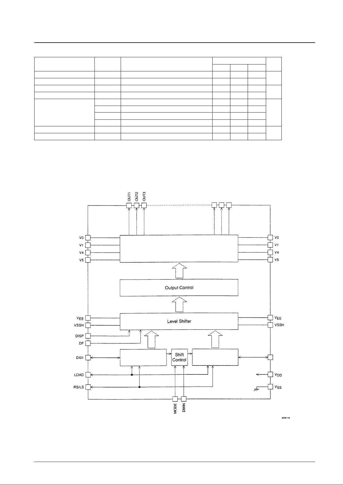
Block Diagram
No. 5953-2/7
LC4131C
Ratings
Parameter Symbol Conditions
min typ max
Unit
Input high-level current I
IH
VIN= VDD*
1
1
µA
Input low-level current I
IL
VIN= VSS*
1
–1
Output high-level voltage V
OH
IOH= –0.4 mA, DIO1, DIO120
0.8 × V
DD
V
DD
V
Output low-level voltage V
OL
IOL= 0.4 mA, DIO1, DIO120 V
SS
0.2 × V
DD
RON0 V
OUT
= V0 – 0.5 V *2, OUT1 to 120 1000
Output on resistance
RON1 V
OUT
= V1 – 0.5 V *2, OUT1 to 120 1000
Ω
RON4 V
OUT
= V4 + 0.5 V *2, OUT1 to 120 1000
RON5 V
OUT
= V5 + 0.5 V *2, OUT1 to 120 1000
Current drain 1 I
DD
VDD*3 200
µA
Current drain 2 I
DDH
VDD*4 500
4-Level LCD Driver Circuit (120 bits)
OUT118
OUT119
OUT120
Bidirectional Shift
Register (60 bits)
Bidirectional Shift
Register (60 bits)
DIO120

Switching Characteristics at VDD= 2.7 to 5.5 V, Ta = –20 to +75°C, VSS= 0 V
Switching Characteristics
No. 5953-3/7
LC4131C
Ratings
Parameter Symbol Conditions
min typ max
Unit
Clock frequency fload LOAD 2.5 MHz
High-level clock pulse width twl LOAD 100
Input setup time tsu LOAD, DIOn, DMIN 100
Input hold time th LOAD, DIOn, DMIN 30
ns
LOAD rise time tr LOAD 30
LOAD fall time tf LOAD 30
DIO output delay time tpld LOAD, DIOn: 30 pF capacitance load 200
LOAD-on delay time tplo LOAD, OUTn: 100 pF capacitance load 1.0
µs
DF-on delay time tpdfo DF, OUTn: 100 pF capacitance load 1.0
DIO output

Pin Functions
No. 5953-4/7
LC4131C
Symbol I/O Function
OUT1 to
OUT120
V0
V1
V4
V5
V
EE
V
SSH
DISP
DF
LOAD
MODE
RS/LS
DIO1
DMIN
DIO120
V
DD
V
SS
O
I
I
I
I
–
–
I
I
I
I
I
I/O
I
I/O
——Logic system power supply
Logic system ground
LCD drive outputs
V0 level drive voltage input
V1 level drive voltage input
V4 level drive voltage input
V5 level drive voltage input
High-voltage block power supply
High-voltage block ground
All outputs will be held at a fixed V5 level when this pin is low.
Alternation input
Data shift pulse input (falling edge)
Data shift direction specification input
*: don’t care
DF Data DISP OUTn
L H H V0
H L H V1
L L H V4
H H H V5
* * L V5
MODE RS/LS Shift direction DIO1 DIO160 DMIN
L L OUT120 →OUT1 OUT IN *
L H OUT1 → OUT120 IN OUT *
H L
OUT120 → OUT61
OUT IN IN
OUT60 → OUT1
H H
OUT1 → OUT60
IN OUT IN
OUT61 → OUT120
*: don’t care (Must be fixed at low or high.)

Pad Assignment
No. 5953-5/7
LC4131C
Chip size : 12.11 x 2.00 mm

LC4131C Pad Coordinates
No. 5953-6/7
LC4131C
Continued on next page.
Pad type Size
A 120 µm × 60 µm
B 75 µm × 60 µm
C 100 µm × 60 µm
Pin X coordinate Y coordinate Pad type Pin X coordinate Y coordinate Pad type
OUT1 –5652.9 718.5 B OUT51 –902.9 718.5 B
OUT2 –5557.9 718.5 B OUT52 –807.9 718.5 B
OUT3 –5462.9 718.5 B OUT53 –712.9 718.5 B
OUT4 –5367.9 718.5 B OUT54 –617.9 718.5 B
OUT5 –5272.9 718.5 B OUT55 –522.9 718.5 B
OUT6 –5177.9 718.5 B OUT56 –427.9 718.5 B
OUT7 –5082.9 718.5 B OUT57 –332.9 718.5 B
OUT8 –4987.9 718.5 B OUT58 –237.9 718.5 B
OUT9 –4892.9 718.5 B OUT59 –142.9 718.5 B
OUT10 –4797.9 718.5 B OUT60 –47.9 718.5 B
OUT11 –4702.9 718.5 B OUT61 47.1 718.5 B
OUT12 –4607.9 718.5 B OUT62 142.1 718.5 B
OUT13 –4512.9 718.5 B OUT63 237.1 718.5 B
OUT14 –4417.9 718.5 B OUT64 332.1 718.5 B
OUT15 –4322.9 718.5 B OUT65 427.1 718.5 B
OUT16 –4227.9 718.5 B OUT66 522.1 718.5 B
OUT17 –4132.9 718.5 B OUT67 617.1 718.5 B
OUT18 –4037.9 718.5 B OUT68 712.1 718.5 B
OUT19 –3942.9 718.5 B OUT69 807.1 718.5 B
OUT20 –3847.9 718.5 B OUT70 902.1 718.5 B
OUT21 –3752.9 718.5 B OUT71 997.1 718.5 B
OUT22 –3657.9 718.5 B OUT72 1092.1 718.5 B
OUT23 –3562.9 718.5 B OUT73 1187.1 718.5 B
OUT24 –3467.9 718.5 B OUT74 1282.1 718.5 B
OUT25 –3372.9 718.5 B OUT75 1377.1 718.5 B
OUT26 –3277.9 718.5 B OUT76 1472.1 718.5 B
OUT27 –3182.9 718.5 B OUT77 1567.1 718.5 B
OUT28 –3087.9 718.5 B OUT78 1622.1 718.5 B
OUT29 –2992.9 718.5 B OUT79 1757.1 718.5 B
OUT30 –2897.9 718.5 B OUT80 1852.1 718.5 B
OUT31 –2802.9 718.5 B OUT81 1947.1 718.5 B
OUT32 –2707.9 718.5 B OUT82 2042.1 718.5 B
OUT33 –2612.9 718.5 B OUT83 2137.1 718.5 B
OUT34 –2517.9 718.5 B OUT84 2232.1 718.5 B
OUT35 –2422.9 718.5 B OUT85 2327.1 718.5 B
OUT36 –2327.9 718.5 B OUT86 2422.1 718.5 B
OUT37 –2232.9 718.5 B OUT87 2517.1 718.5 B
OUT38 –2137.9 718.5 B OUT88 2612.1 718.5 B
OUT39 –2042.9 718.5 B OUT89 2707.1 718.5 B
OUT40 –1947.9 718.5 B OUT90 2802.1 718.5 B
OUT41 –1852.9 718.5 B OUT91 2897.1 718.5 B
OUT42 –1757.9 718.5 B OUT92 2992.1 718.5 B
OUT43 –1662.9 718.5 B OUT93 3087.1 718.5 B
OUT44 –1567.9 718.5 B OUT94 3182.1 718.5 B
OUT45 –1472.9 718.5 B OUT95 3277.1 718.5 B
OUT46 –1377.9 718.5 B OUT96 3372.1 718.5 B
OUT47 –1282.9 718.5 B OUT97 3467.1 718.5 B
OUT48 –1187.9 718.5 B OUT98 3562.1 718.5 B
OUT49 –1092.9 718.5 B OUT99 3657.1 718.5 B
OUT50 –997.9 718.5 B OUT100 3752.1 718.5 B

Continued from preceding page.
PS No. 5953-7/7
LC4131C
Pin X coordinate Y coordinate Pad type
OUT101 3847.1 718.5 B
OUT102 3942.1 718.5 B
OUT103 4037.1 718.5 B
OUT104 4132.1 718.5 B
OUT105 4227.1 718.5 B
OUT106 4322.1 718.5 B
OUT107 4417.1 718.5 B
OUT108 4512.1 718.5 B
OUT109 4607.1 718.5 B
OUT110 4702.1 718.5 B
OUT111 4797.1 718.5 B
OUT112 4892.1 718.5 B
OUT113 4987.1 718.5 B
OUT114 5082.1 718.5 B
OUT115 5177.1 718.5 B
OUT116 5272.1 718.5 B
OUT117 5367.1 718.5 B
OUT118 5462.1 718.5 B
OUT119 5557.1 718.5 B
OUT120 5652.1 718.5 B
V4 –5713.8 –790.8 A
V4 –5433.8 –790.8 A
V
EE
–4033.8 –813.8 A
V
EE
–3753.8 –813.8 A
V
SSH
–3473.8 –811.2 A
V
SSH
–3193.8 –811.2 A
MODE –2911.0 –804.0 A
Dammy –2631.0 –804.0 A
RSLS –2347.2 –804.0 A
Dammy –2065.4 –804.0 A
V
DD
–1782.6 –804.0 A
V
DD
–1605.4 –804.0 A
DISP –1219.8 –804.0 A
Dammy –939.8 –804.0 A
DF –654.2 –804.0 A
Dammy –374.2 –804.0 A
V
SS
–91.4 –804.0 A
Pin X coordinate Y coordinate Pad type
V
SS
88.6 –804.0 A
LOAD 475.2 –804.0 A
Dammy 757.0 –804.0 A
Dammy 1502.6 –804.0 A
DIO1 1785.4 –804.0 A
Dammy 2065.4 –804.0 A
DMIN 2348.2 –804.0 A
Dammy 2631.0 –804.0 A
DIO120 2913.8 –804.0 A
V
SSH
3196.6 –803.8 A
V
SSH
3476.6 –803.8 A
V
EE
3756.6 –823.8 A
V
EE
4036.6 –823.8 A
V0 4316.6 –813.8 A
V0 4596.6 –813.8 A
V1 4876.6 –791.0 A
V1 5156.6 –791.0 A
V4 5436.6 –790.1 A
V4 5716.6 –790.1 A
V
SS
1039.8 –783.6 A
V
SS
1219.8 –783.6 A
V1 –5153.8 –786.9 A
V1 –4873.8 –786.9 A
V0 –4593.8 –786.9 A
V0 –4313.8 –786.9 A
V5 5895.0 –462.5 C
V5 –5891.7 –459.5 C
V5 5895.0 –322.5 C
V5 –5891.7 –319.5 C
V5 5895.0 –182.5 C
V5 –5891.7 –179.5 C
V
SSH
–5885.7 87.5 C
V
SSH
5885.6 87.5 C
V
SSH
–5885.7 227.5 C
V
SSH
5885.6 227.5 C
V
SSH
–5885.7 367.5 C
V
SSH
5885.6 367.5 C
This catalog provides information as of April, 1998. Specifications and information herein are subject to change
without notice.
■ No products described or contained herein are intended for use in surgical implants, life-support systems, aerospace
equipment, nuclear power control systems, vehicles, disaster/crime-prevention equipment and the like, the failure of
which may directly or indirectly cause injury, death or property loss.
■ Anyone purchasing any products described or contained herein for an above-mentioned use shall:
➀ Accept full responsibility and indemnify and defend SANYO ELECTRIC CO., LTD., its affiliates, subsidiaries and
distributors and all their officers and employees, jointly and severally, against any and all claims and litigation and all
damages, cost and expenses associated with such use:
➁ Not impose any responsibility for any fault or negligence which may be cited in any such claim or litigation on
SANYO ELECTRIC CO., LTD., its affiliates, subsidiaries and distributors or any of their officers and employees
jointly or severally.
■ Information (including circuit diagrams and circuit parameters) herein is for example only; it is not guaranteed for
volume production. SANYO believes information herein is accurate and reliable, but no guarantees are made or implied
regarding its use or any infringements of intellectual property rights or other rights of third parties.
 Loading...