

Page 1
Any and all SANYO products described or contained herein do not have specifications that can handle
applications that require extremely high levels of reliability, such as life-support systems, aircraft’s
control systems, or other applications whose failure can be reasonably expected to result in serious
physical and/or material damage. Consult with your SANYO representative nearest you before using
any SANYO products described or contained herein in such applications.
SANYO assumes no responsibility for equipment failures that result from using products at values that
exceed, even momentarily, rated values (such as maximum ratings, operating condition ranges, or other
parameters) listed in products specifications of any and all SANYO products described or contained
herein.
Overview
The LC4104C-T2A is a segment driver IC for large-scale
dot matrix LCD displays. The LC4104C-T2A latches 160bits of display data transferred from the controller over a
4- or 8-bit parallel interface and generates the LCD drive
signals. In conjunction with the LC4102C-T2A common
driver, the LC4104C-T2A forms a chip set that can drive
large-screen LCD panels.
Features
• High-voltage CMOS (P-sub) process
• LCD drive voltage: 36 V
• Logic system power-supply voltage: 2.7 to 5.5 V
• Maximum fcp: 12 MHz (VDD= 5 V ±10%),
10 MHz (VDD= 2.7 to 4.5 V)
• Parallel input circuit can be switched between 4 and
8 bits.
• Output directionality switching
• DISPOFF function (Holds the LCD drive voltage at a
fixed level.)
• Display duty ratios: 1/160 to 1/480
• Package: TCP (Tape Carrier Package)
CMOS IC
Ordering number : ENN*6790
20702TN (OT) No. 6790-1/8
Preliminary
SANYO Electric Co.,Ltd. Semiconductor Company
TOKYO OFFICE Tokyo Bldg., 1-10, 1 Chome, Ueno, Taito-ku, TOKYO, 110-8534 JAPAN
LCD Dot Matrix Segment Driver for STN Displays
LC4104C-T2A
Page 2
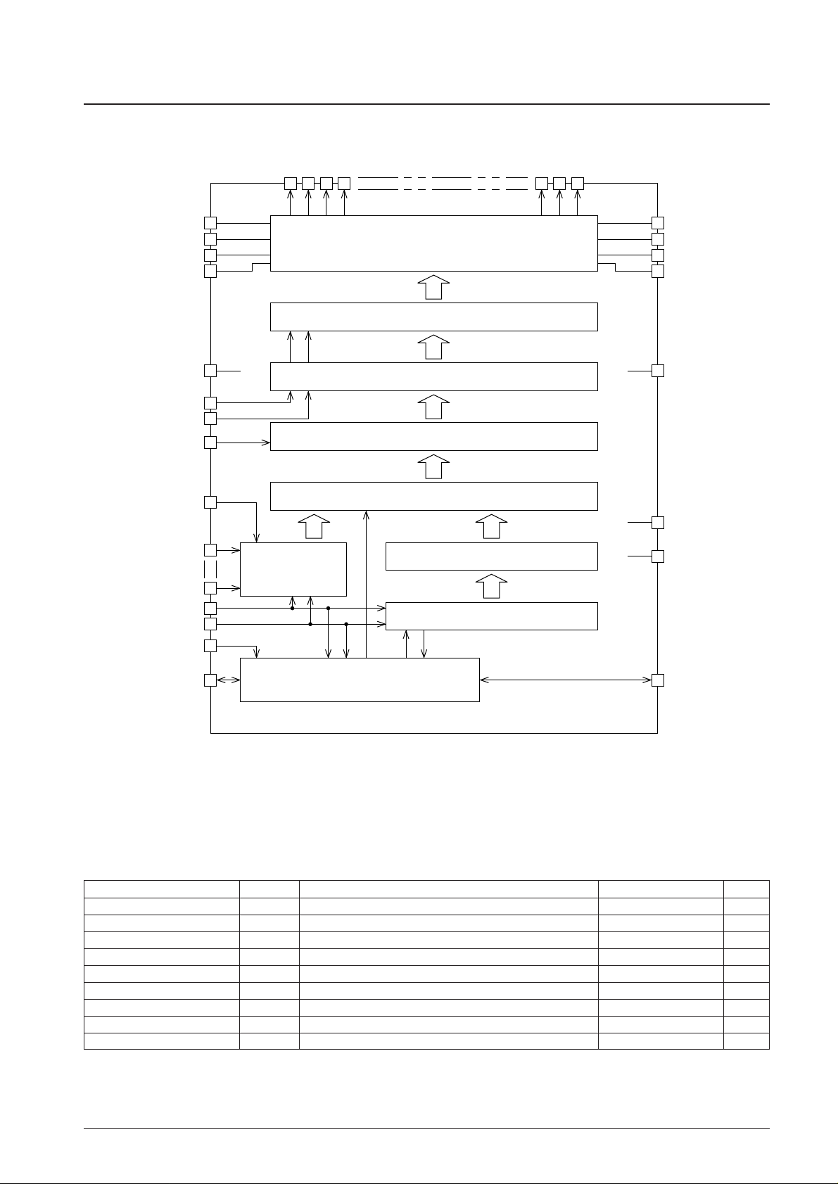
Block Diagram
Specifications
The following electrical characteristics apply when sealed in a SANYO standard PGA-208 package.
Absolute Maximum Ratings at VSS= 0 V
Note: V0, V2, V3, and V5 must obey the following relationships: V
DDH
≥ V0 ≥V2 ≥ V
DDH
– 7 V, and 7 V ≥ V3 ≥ V5 ≥ VSS.
No. 6790-2/8
LC4104C-T2A
Parameter Symbol Conditions Ratings Unit
Maximum supply voltage V
DD
max –0.3 to +7 V
Maximum supply voltage V
DDH
max –0.3 to +40 V
Maximum supply voltage V
SS
max –0.3 to +0.3 V
Input voltage V
IN
D0 to D7, LOAD, CP, R/L, TEST, DISP, M, EIO1, EIO2, BS –0.3 to VDD+ 0.3 V
Input voltage V0, V2 V0, V2 V
DDH
– 7 to V
DDH
+ 0.3 V
Input voltage V3 V3 –0.3 to V
SS
+ 7 V
Input voltage V5 V5 –0.3 to +0.3 V
Operating temperature Topr –20 to +75 °C
Storage temperature Tstg –55 to +125 °C
V0
V2
V3
VDDH
LOAD
BS
DISP
M
V5
V0
V2
V3
VDDH
V
DD
V
SS
EIO2
V5
O1
TEST
D0
D7
EIO1
CP
R/L
O2O3O4
O158
O159
O160
Output Control
4 Level LCD Drive Circuit (160bits)
Level Shifter
2nd Latch (160bits)
1st Latch (8bits × 20)
Address Decoder
Address Counter
—
A1367
Bits
Control
Chip Disable &
Latch Control
Page 3
Allowable Operating Ranges at Ta = –20 to +75°C, VSS= 0 V
Note: V0, V2, V3, and V5 must obey the following relationships: V
DDH
≥ V0 ≥ V2 ≥ V
DDH
– 7 V, and 7 V ≥ V3 ≥ V5 ≥ VSS.
At power on: First turn on the logic system power supply and then turn on the high-voltage system power supply; alternatively, turn both on at the
same time.
At power off: First turn off the high-voltage system power supply and then turn off the logic system power supply; alternatively, turn both off at the
same time.
Allowable Operating Ranges at Ta = –20 to +75°C, VSS= 0 V, VDD= 5 V ± 10%
Note: * The clock rise time (tr) and fall time (tf) must obey inequalities ➀ and ② below.
➀: tr, tf <
②: tr, tf ≤ 50 ns
Allowable Operating Ranges at Ta = –20 to +75°C, VSS= 0 V, VDD= 2.7 to 4.5 V
Note: * The clock rise time (tr) and fall time (tf) must obey inequalities ➀ and ② below.
➀: tr, tf <
②: tr, tf ≤ 50 ns
1
– tw (cph) – tw (cpl)
fcp
2
1
– tw (cph) – tw (cpl)
fcp
2
No. 6790-3/8
LC4104C-T2A
Parameter Symbol Conditions
Ratings
Unit
min typ max
Supply voltage V
DD
2.7 5.5 V
Supply voltage V
DDH
14 36 V
Supply voltage V
SS
0 V
Input high-level voltage V
IH
D0 to D7, LOAD, CP, R/L, M, TEST, DISP, BS,
0.8 V
DD
V
DD
V
EIO1, EIO2
Input low-level voltage V
IL
D0 to D7, LOAD, CP, R/L, M, TEST, DISP, BS,
0 0.2 V
DD
V
EIO1, EIO2
Input voltage V0, V2 V0, V2 V
DDH
– 7 V
DDH
V
Input voltage V3 V3 0 V
SSH
+ 7 V
Input voltage V5 V5 0 V
Parameter Symbol Conditions
Ratings
Unit
min typ max
CP clock frequency fcp CP 12 MHz
High-level load pulse width tw (ldH) LOAD 50 ns
High-level clock pulse width tw (cpH) CP 20 ns
Low-level clock pulse width tw (cpL) CP 20 ns
LOAD/CP setup time tsu (ld) LOAD, CP 100 ns
LOAD/CP hold time tho (ld) LOAD, CP 200 ns
DATA/CP setup time tsu (cp) CP, D0 to D7 10 ns
DATA/CP hold time tho (cp) CP, D0 to D7 10 ns
EIO input setup time tsu (ei) CP, EIO1, EIO2 24 ns
Clock rise time tr LOAD, CP* 50 ns
Clock fall time tf LOAD, CP* 50 ns
Parameter Symbol Conditions
Ratings
Unit
min typ max
CP clock frequency fcp CP 10 MHz
High-level load pulse width tw (ldH) LOAD 50 ns
High-level clock pulse width tw (cpH) CP 37 ns
Low-level clock pulse width tw (cpL) CP 37 ns
LOAD/CP setup time tsu (ld) LOAD, CP 100 ns
LOAD/CP hold time tho (ld) LOAD, CP 200 ns
DATA/CP setup time tsu (cp) CP, D0 to D7 35 ns
DATA/CP hold time tho (cp) CP, D0 to D7 35 ns
EIO input setup time tsu (ei) CP, EIO1, EIO2 30 ns
Clock rise time tr LOAD, CP* 50 ns
Clock fall time tf LOAD, CP* 50 ns
Page 4

Electrical Characteristics at Ta = –20 to +75°C, VDD= 2.7 to 5.5 V, VSS= 0 V
Note: 1. VOis the voltage applied for an on output, V0 = V
DDH
, V2 = 18/20 (V
DDH
– VSS), V3 = 2/20 (V
DDH
– VSS), V5 = V
SS
2. LOAD = 28 kHz, CP = 10 MHz, M = 75 Hz
Alternatively: No output load and with the inputs V
IH
= VDDand VIL= VSS.
3. The current drain in standby mode. Note that the EIOn pins must be held at V
DD
.
Switching Characteristics at Ta = –20 to +75°C, VSS= 0 V, VDD= 5 V ± 10%
Switching Characteristics at Ta = –20 to +75°C, VSS= 0 V, VDD= 2.7 to 4.5 V
Timing Chart
No. 6790-4/8
LC4104C-T2A
Parameter Symbol Conditions
Ratings
Unit
min typ max
Input high-level current
I
IH
VIN= VDD: D0 to D7, LOAD, CP, R/L, M, DISP,
5 µA
EIO1, EIO2, BS, TEST
I
IL
1 VIN= VSS: D0 to D7, LOAD, CP, R/L, M, DISP, –5
Input low-level current EIO1, EIO2, BS µA
IIL2 VIN= VSS: TEST –500
Output high-level voltage V
OH
IO= –0.4 mA: EIO1, EIO2 VDD– 0.4 V
DD
V
Output low-level voltage V
OL
IO= 0.4 mA: EIO1, EIO2 V
SS
0.4 V
Output on resistance R
OUT
V
DDH
= 36 V*1, V0 – VO= 0.5 V, V2 – VO= 0.5 V,
1 3 kΩ
V
O
– V3 = 0.5 V, VO– V5 = 0.5 V: O1 to O160
I
DD
VDD= 2.7 to 5.5 V 5.0 mA
Current drain I
DDH
VDD= 2.7 to 5.5 V, V
DDH
= 32 V*2,
2.0 mA
V
DD
= 5 V ± 10%, V
DDH
= 36 V
2.0 mA
I
ST
*3 500 µA
Parameter Symbol Conditions
Ratings
Unit
min typ max
EIO output delay time td (eo) 30 pF capacitive load: CP, EIO1, EIO2 40 ns
LD/EIO output delay time td (leo) 30 pF capacitive load: LOAD, EIO1, EIO2 70 ns
LOAD/on delay time td (ldo) 100 pF capacitive load: LOAD, O1 to O160 3 µs
M/on delay time td (mo) 100 pF capacitive load: M, O1 to O160 3 µs
Parameter Symbol Conditions
Ratings
Unit
min typ max
EIO output delay time td (eo) 30 pF capacitive load: CP, EIO1, EIO2 80 ns
LD/EIO output delay time td (leo) 30 pF capacitive load: LOAD, EIO1, EIO2 130 ns
LOAD/on delay time td (ldo) 100 pF capacitive load: LOAD, O1 to O160 3 µs
M/on delay time td (mo) 100 pF capacitive load: M, O1 to O160 3 µs
LOAD
CP
D0 to D7
tr(ld) tf(ld)
0.8V
0.2V
M
DD
DD
tw(ldH)
tsu(ld)
tho(ld)
td(ldo)
td(mo)
tsu(cp)
tho(cp)
tr(cp) tf(cp)
tw(cpH)
tw(cpL)
On
EIOn (output)
(Input to the
next stage)
td(leo)
td(eo)
tsu(ei)
A13677
Page 5

Pin Functions
No. 6790-5/8
LC4104C-T2A
Symbol I/O Function
O1 to O160
V0
V2
V3
V5
V
DDH
V
DD
V
SS
DISP
M
EIO1
EIO2
CP
LOAD
TEST
R/L
D0 to D7
BS
O
I
I
I
I
—
—
—
I
I
I/O
I/O
I
I
I
I
I
I
LCD drive outputs
V0 level drive voltage supply (selected level)
V2 level drive voltage supply (unselected level)
V3 level drive voltage supply (unselected level)
V5 level drive voltage supply (selected level)
High-voltage system power supply.
Logic system power supply.
GND
LCD off function. All outputs go to the V5 level when this pin is low.
Alternation signal input
Enable I/O
Enable input: The enable input at the first stage is fixed at V
SS
. For succeeding stages, the enable input is connected to the
enable output from the preceding stage.
Enable output: Connected to the enable input of the next stage when cascode connection is used.
Data acquisition clock (falling edge)
Data load clock (falling edge)
Test input. Must be tied high in normal use.*
Data shift direction setting
Parallel data inputs
Input bus setting. Set high for 8-bit input, low for 4-bit input. For 4-bit input, D0 to D3 are used for data input and D4 to D7 must
be tied to ground.
*: Don’t care.
M Data DISP On
H H H V0
H L H V2
L L H V3
L H H V5
* * L V5
R/L EIO1 EIO2
L In Out
H Out In
R/L BS O1 to O160 outputs
O1 O2 O3 O4
→ . . . O157 O158 O159 O160
L
↑ ↑ ↑ ↑ ↑ ↑ ↑ ↑
H
D7 D6 D5 D4 D3 D2 D1 D0
O1 O2 O3 O4 . . .← O157 O158 O159 O160
H
↑ ↑ ↑ ↑ ↑ ↑ ↑ ↑
D0 D1 D2 D3 D4 D5 D6 D7
O1 O2 O3 O4 → . . . O157 O158 O159 O160
L
↑ ↑ ↑ ↑ ↑ ↑ ↑ ↑
L
D3 D2 D1 D0 D3 D2 D1 D0
O1 O2 O3 O4 . . .← O157 O158 O159 O160
H
↑ ↑ ↑ ↑ ↑ ↑ ↑ ↑
D0 D1 D2 D3 D0 D1 D2 D3
Page 6

Pin Assignment
No. 6790-6/8
LC4104C-T2A
DUMMY
LC4104C-T2A
(CHIP Top VIEW)
V3
V5
V2
V3
V5
A13678
DISP
D6
V
DD
CP
LOAD
M
D7
EIO2
EIO1
D1
R/L
D2
D3
D4
D5
V
DDH
V0
V2
VDDH
V0
VSS
D0
BS
OUT160
OUT159
OUT158
DUMMY
OUT3
OUT2
OUT1
Note: This figure shows the chip pattern surface as seen from abobe.
This figure dose not stipulate the TCP package.
Page 7

No. 6790-7/8
LC4104C-T2A
Package Dimensions
unit: mm
LC4104C-T2A
(Cu)
ø2.0
±
0.1
0.6 MAX
LSI chip
Flex hole
0.3 MAX
0.75 MAX
1.35 MAX
0.4
±
0.05
ø1.0
±
0.05
0.4
±
0.02
0.6
±
0.02
1.981
±
0.03
4.75(P)
×
4=19.0
±
0.05
4.75
±
0.03
1.2
±
0.05(SL)
2.0
±
0.05(SL)
4.48 MAX(Sealing area)
1.98(LSI)
2.48
±
0.05
8.0
±
0.1(SL)
4.0
±
0.1(SL)
R0.8
±
0.3(SR)
R0.5
±
0.05
0.6 MAX
0.6 MAX
0.3
±
0.05
10.3
±
0.05
3.7(
Cut line
)
8.5
±
0.3(SR)
1.7
±
0.3(SR)
1.2
±
0.05(SL)
6.7
±
0.05(SL)
1.2
±
0.05(SL)
4.9
±
0.05(SL)
15.0
19.8
±
0.119.8
±
0.1
1.7
±
0.1(SL)
1.7
±
0.1(SL)
12.55
±
0.1(SL)
12.55
±
0.1(SL)
23.6
±
0.05(SL)
24.0
±
0.055
0.14(P)
×
(162--1)=22.54
±
0.055 (W=0.09)
25.5(Cut line)
24.3
±
0.3(SR)
23.0
±
0.05(SL)
22.0
±
0.05(SL)
13.05(LSI)
13.55
±
0.05(Device hole)
15.55 MAX(Sealing area)
0.8(P)
×
(28--1)=21.6
±
0.055 (W=0.34)
32.0
±
0.1
48.175
±
0.2
42.177
±
0.07
V5
V5
V3
VDDH
V2
V0
D0
D1
D2
D3
D4
D5
D6
D7
VDD
EIO2
EI01
CP
LOAD
M
DISP
R/L
BS
VSS
VDDH
V0
V2
V3
Device hole
Sealing area
Page 8

PS No. 6790-8/8
LC4104C-T2A
This catalog provides information as of February, 2002. Specifications and information herein are subject
to change without notice.
Specifications of any and all SANYO products described or contained herein stipulate the performance,
characteristics, and functions of the described products in the independent state, and are not guarantees
of the performance, characteristics, and functions of the described products as mounted in the customer’s
products or equipment. To verify symptoms and states that cannot be evaluated in an independent device,
the customer should always evaluate and test devices mounted in the customer’s products or equipment.
SANYO Electric Co., Ltd. strives to supply high-quality high-reliability products. However, any and all
semiconductor products fail with some probability. It is possible that these probabilistic failures could
give rise to accidents or events that could endanger human lives, that could give rise to smoke or fire,
or that could cause damage to other property. When designing equipment, adopt safety measures so
that these kinds of accidents or events cannot occur. Such measures include but are not limited to protective
circuits and error prevention circuits for safe design, redundant design, and structural design.
In the event that any or all SANYO products (including technical data, services) described or contained
herein are controlled under any of applicable local export control laws and regulations, such products must
not be exported without obtaining the export license from the authorities concerned in accordance with the
above law.
No part of this publication may be reproduced or transmitted in any form or by any means, electronic or
mechanical, including photocopying and recording, or any information storage or retrieval system,
or otherwise, without the prior written permission of SANYO Electric Co., Ltd.
Any and all information described or contained herein are subject to change without notice due to
product/technology improvement, etc. When designing equipment, refer to the “Delivery Specification”
for the SANYO product that you intend to use.
Information (including circuit diagrams and circuit parameters) herein is for example only; it is not
guaranteed for volume production. SANYO believes information herein is accurate and reliable, but
no guarantees are made or implied regarding its use or any infringements of intellectual property rights
or other rights of third parties.
 Loading...