

Page 1

Any and all SANYO products described or contained herein do not have specifications that can handle
applications that require extremely high levels of reliability, such as life-support systems, aircraft’s
control systems, or other applications whose failure can be reasonably expected to result in serious
physical and/or material damage. Consult with your SANYO representative nearest you before using
any SANYO products described or contained herein in such applications.
SANYO assumes no responsibility for equipment failures that result from using products at values that
exceed, even momentarily, rated values (such as maximum ratings, operating condition ranges,or other
parameters) listed in products specifications of any and all SANYO products described or contained
herein.
CMOS (P-sub)
STN LCD Dot Matrix Common Driver
Ordering number:ENN*5193B
LC4103TAB-01, 4103TAB-02, 4103C
SANYO Electric Co.,Ltd. Semiconductor Company
TOKYO OFFICE Tokyo Bldg., 1-10, 1 Chome, Ueno, Taito-ku, TOKYO, 110-8534 JAPAN
Preliminary
Overview
The LC4103 is a common driver IC for large-scale dot matrix LCD displays, It includes a 160-bit bidirectional shift
register and 4-level LCD drivers. The number of bits can
be increased by using the I/O pins provided for cascode
connection. In conjunction with the LC4104 segment driver ,
the LC4103 forms a chip set that can drive large-screen
LCD panels.
Features
• High-voltage CMOS (P-sub) process.
• LCD drive voltage : 42V
• Logic system power-supply voltage : 2.7 to 5.5V
• Maximum fcp : 2.5MHz (V
• Bidirectional shift register.
• The shift register can be divided into two 80-bit registers
(thus allowing two-screen drive).
• DISPOFF function (Holds the LCD drive voltage at a f ixed
level).
• Slim TAB (160 outputs).
• Display duty ratios : 1/160 to 1/480.
• Package lineup.
200kHz (V
=5V±10%),
DD
=2.7 to 4.5V)
DD
.oNepyTegakcaP
10-BAT3014CLhctipdaelretuomµ052:BAT
20-BAT3014CLhctipdaelretuomµ081:BAT
C3014CLtcudorppihC
62001TN (KT)/D3095HA (OT) No.5193–1/11
Page 2
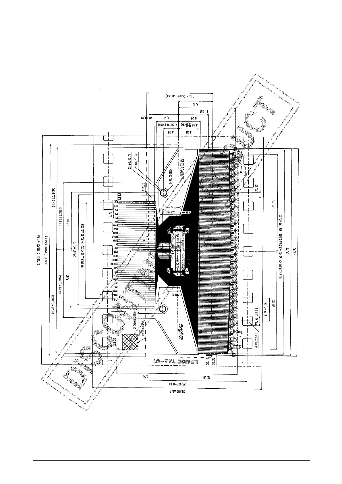
Package Dimensions
unit:mm
LC4103TAB-01
LC4103TAB-01, 4103TAB-02, 4103C
No.5193–2/11
Page 3
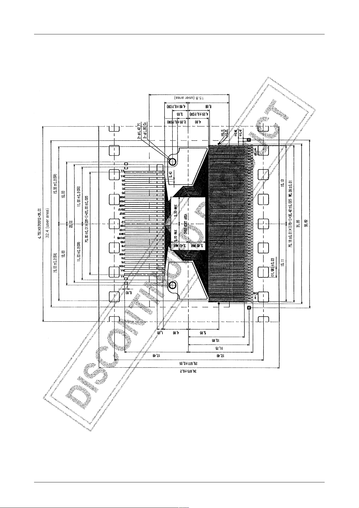
LC4103TAB-02
LC4103TAB-01, 4103TAB-02, 4103C
No.5193–3/11
Page 4
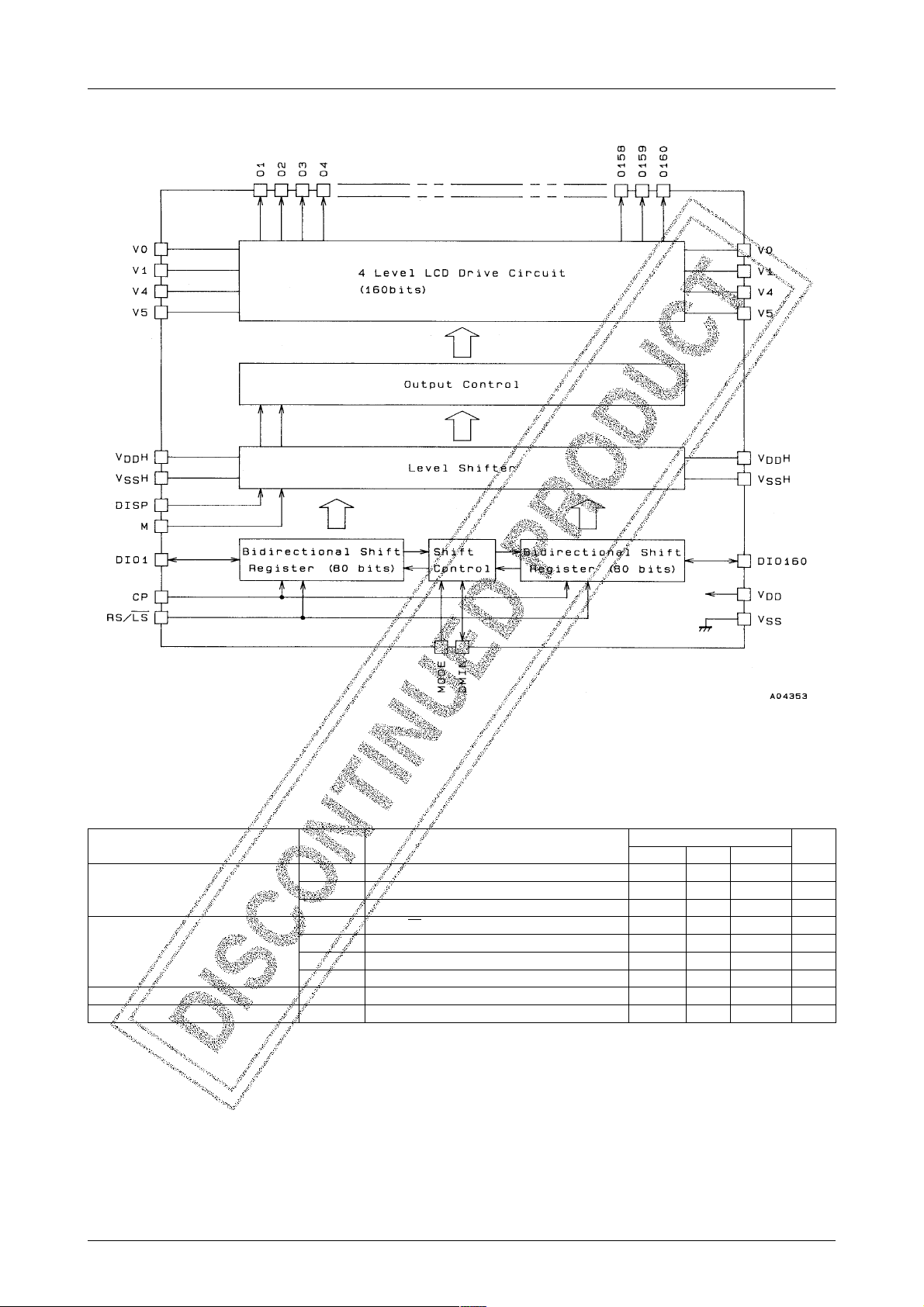
Block Diagram
LC4103TAB-01, 4103TAB-02, 4103C
Specifications
The following electrical characteristics apply when sealed in a SANYO standard PGA-208 package.
Absolute Maximum Ratings at V
retemaraPlobmySsnoitidnoC
egatlovylppusmumixaM
egatlovtupnI
erutarepmetgnitarepOrpoT 02– 57+
erutarepmetegarotSgtsT55– 521+
Note : * V0, V1, V4, and V5 must obey the following inequalities : V
=0V
SS
nimpytxam
V
xamV
DD
V
HDD
V
HSS
V
NI
4V4V,*3.0– VSS7+V
5V5V,*3.0– 3.0+V
DD
xamV
HDD
xamV
HSS
1V,0V1V,0V,*V
≥V0≥V1≥V
DDH
DDH
NIMD,061OID,0OID,M,PSID,SL/SR,PC3.0– V
–7V, and 7V≥V4≥V5≥V
3.0– 7+V
3.0– 54+V
3.0– 3.0+V
7– V
HDD
.
SSH
sgnitaR
DD
HDD
tinU
3.0+V
3.0+V
˚C
˚C
No.5193–4/11
Page 5

LC4103TAB-01, 4103TAB-02, 4103C
Allowable Operating Ranges at Ta =–20 to +75˚C, VSS=0V
retemaraPlobmySsnoitidnoC
V
egatlovylppuS
egatlovlevel-hgihtupnIV
egatlovlevel-woltupnIV
egatlovtupnI
V
V
Note : V0, V1, V4, and V5 must obey the following inequalities : V
At power on : First turn on the logic system power supply and then turn on the high-voltage system power supply.
At power off : First turn off the high-voltage system power supply and then turn off the logic system power supply.
Allowable Operating Ranges at VDD=5V±10%
retemaraPlobmySsnoitidnoC
ycneuqerfkcolCpcfPC 5.2zHM
htdiweslupkcolclevel-hgiHcwtPC03sn
emitputestupnIustNIMD,061OID,0OID,PC001sn
enildlohtupnIhtNIMD,061OID,0OID,PC03sn
emitesirPCrtPC 03sn
emitllafPCftPC 03sn
V
DD
HI
LI
4V4V,*0V
5V5V,*0V
DD
V
HDD
HSS
1V,0V1V,0V,*V
HDD
V
HSS
≥V0≥V1≥V
DDH
–7V, and 7V≥V4≥V5≥V
DDH
sgnitaR
nimpytxam
7.25.5V
0224V
0V
EDOM,NIMD,PC,061OID,1OID,M,PSID,SL/SRV8.0
EDOM,NIMD,PC,061OID,1OID,M,PSID,SL/SR0V2.0
SSH
DD
HDD
.
7– V
sgnitaR
nimpytxam
V
DD
DD
HDD
7+V
HSS
tinU
V
V
V
tinU
Allowable Operating Ranges at VDD=2.7 to 4.5V
retemaraPlobmySsnoitidnoC
ycneuqerfkcolCpcfPC 002zHk
htdiweslupkcolclevel-hgiHcwtPC001sn
emitputestupnIustNIMD,061OID,0OID,PC001sn
emitdlohtupnIhtNIMD,061OID,0OID,PC03sn
emitesirPCrtPC 03sn
emitllafPCftPC 03sn
Electrical Characteristics at Ta =–20 to +75˚C, V
retemaraPlobmySsnoitidnoC
tnerruclevel-hgihtupnII
tnerruclevel-woltupnII
egatlovlevel-hgihtuptuOV
egatlovlevel-woltuptuOV
ecnatsisernotuptuOR
1niardtnerruCI
2niardtnerruCI
Note : * VO is the voltage applied for an on output, V0=V
HI
LI
HO
LO
TUO
DD
HDD
DDH
VNIV=
VNIV=
I
O
I
O
V
V
O
V
V
, V1=19/20 (V
=2.7 to 5.5V, VSS=0V
DD
DD
EDOM,NIMD
SS
EDOM,NIMD
HDD
DD
DD
V–0V,*,V04=
O
V,V5.0=4V–
O
DDH–VSSH
061Oot1O:V7.2=
sgnitaR
nimpytxam
sgnitaR
nimpytxam
,061OID,0OID,M,PSID,SL/SR,PC:
,061OID,0OID,M,PSID,SL/SR,PC:
061OID,1OID:Am4.0–=
061OID,1OID:Am4.0=V
V–1V,V5.0=
,V5.0=
O
,V5.0=5V–
zHk05=pcf,V5.5ot7.2= 002Aµ
V,daoltuptuoon,zH001=Mf
HDD
), V4=1/20 (V
DDH–VSSH
tfihsatad1,V24=005Aµ
1– Aµ
V8.0
DD
SS
), V5=V
SSH
, V
SSH=VSS
V
V2.0
.
1Aµ
DD
DD
0.1kΩ
tinU
tinU
V
V
No.5193–5/11
Page 6

LC4103TAB-01, 4103TAB-02, 4103C
Switching Characteristics at Ta =–20 to +75˚C, VSS=0V, VDD=5V±10%
retemaraPlobmySsnoitidnoC
emityaledtuptuoOIDDCPtdaoleviticapacFp03 09sn
emityalednO/PCOCPtdaoleviticapacFp001 007sn
emityalednO/MOMPtdaoleviticapacFp001 007sn
Switching Characteristics at Ta =–20 to +75˚C, VSS=0V, VDD=2.7 to 4.5V
retemaraPlobmySsnoitidnoC
emityaledtuptuoOIDDCPtdaoleviticapacFp03 053sn
emityalednO/PCOCPtdaoleviticapacFp001 3sµ
emityalednO/MOMPtdaoleviticapacFp001 3sµ
Timing Chart
sgnitaR
nimpytxam
sgnitaR
nimpytxam
tinU
tinU
No.5193–6/11
Page 7

Pin Functions
lobmySO/InoitcnuF
061Oot1OO
0V
1V
4V
5V
V
HDD
V
HSS
PSIDI .wolsinipsihtnehwlevel5VehtotogstuptuollA.noitcnufffoDCL
MI .tupnilangisnoitanretlA
PCI .)egdagnillaf(tupniesluptfihsataD
EDOMI
SL/SRI
1OID
NIMD
061OID
LC4103TAB-01, 4103TAB-02, 4103C
stuptuoevirdDCL
MataDPSIDnO
LHH 0V
HLH 1V
LLH4V
HHH 5V
**L5V
I
I
I
I
– .laitnetopemasehtottesebtsumemanemasehthtiwsniP.ylppusrewopmetsysegatlov-hgiH
– .laitnetopemasehtottesebtsumemanemasehthtiwsniP.dnuorgmetsysegatlov-hgiH
MODE RS/LS DIO1 DIO160 DMINData transfer direction
L Out In *O160 → O1
L
H In Out *O1 → O160
O/I
I
O/I
L Out In In
H
H In Out In
O160 → O81
O80 → O1
O1 → O80
O81 → O160
).wolrohgihrehtiedlehebtsuM(.eract'noD:*
)leveldetceles(ylppusegatlovevirdlevel0V
)leveldetcelesnu(ylppusegatlovevirdlevel1V
Pins with the same name must be set to the same potential.
)leveldetcelesnu(ylppusegatlovevirdlevel4V
)leveldetceles(ylppusegatlovevirdlevel5V
V
DD
V
SS
Pin Assignment
).wolrohgihrehtiedlehebtsuM(.eract'noD:*
– ylppusrewopmetsyscigoL
– dnuorgmetsyscigoL
No.5193–7/11
Page 8

Pin Assignment
LC4103TAB-01, 4103TAB-02, 4103C
No.5193–8/11
Page 9

Pad Coordinates
PAD No.
1
2
3
4
5
6
7
8
9
10
11
12
13
14
15
16
17
18
19
20
21
22
23
24
25
26
27
28
29
30
31
32
33
34
35
36
37
38
39
40
Signal
O1
O2
O3
O4
O5
O6
O7
O8
O9
O10
O11
O12
O13
O14
O15
O16
O17
O18
O19
O20
O21
O22
O23
O24
O25
O26
O27
O28
O29
O30
O31
O32
O33
O34
O35
O36
O37
O38
O39
O40
LC4103TAB-01, 4103TAB-02, 4103C
X coordinate
–1800.0
–1880.0
1960.0
–2040.0
–2120.0
–2200.0
–2280.0
–2360.0
–2440.0
–2520.0
–2600.0
–2680.0
–2760.0
–2840.0
–2920.0
–3000.0
–3080.0
–3160.0
–3240.0
–3320.0
–3400.0
–3480.0
–3673.0
–3673.0
–3673.0
–3673.0
–3673.0
–3673.0
–3673.0
–3673.0
–3673.0
–3673.0
–3673.0
–3673.0
–3673.0
–3673.0
–3480.0
–3400.0
–3320.0
–3240.0
Y coordinate
–1425.2
–1425.2
–1425.2
–1425.2
–1425.2
–1425.2
–1425.2
–1425.2
–1425.2
–1425.2
–1425.2
–1425.2
–1425.2
–1425.2
–1425.2
–1425.2
–1425.2
–1425.2
–1425.2
–1425.2
–1425.2
–1425.2
–1497.6
–1417.6
–1337.6
–1257.6
–1177.6
–1097.6
–1017.6
1017.6
1097.6
1177.6
1257.6
1337.6
1417.6
1497.6
1429.2
1429.2
1429.2
1429.2
PAD No.
41
42
43
44
45
46
47
48
49
50
51
52
53
54
55
56
57
58
59
60
61
62
63
64
65
66
67
68
69
70
71
72
73
74
75
76
77
78
79
80
Signal
O41
O42
O43
O44
O45
O46
O47
O48
O49
O50
O51
O52
O53
O54
O55
O56
O57
O58
O59
O60
O61
O62
O63
O64
O65
O66
O67
O68
O69
O70
O71
O72
O73
O74
O75
O76
O77
O78
O79
O80
X coordinate
–3160.0
–3080.0
–3000.0
–2920.0
–2840.0
–2760.0
–2680.0
–2600.0
–2520.0
–2440.0
–2360.0
–2280.0
–2200.0
–2120.0
–2040.0
–1960.0
–1880.0
–1800.0
–1720.0
–1640.0
–1560.0
–1480.0
–1400.0
–1320.0
–1240.0
–1160.0
–1080.0
–1000.0
–920.0
–840.0
–760.0
–680.0
–600.0
–520.0
–440.0
–360.0
–280.0
–200.0
–120.0
–40.0
Y coordinate
1429.2
1429.2
1429.2
1429.2
1429.2
1429.2
1429.2
1429.2
1429.2
1429.2
1429.2
1429.2
1429.2
1429.2
1429.2
1429.2
1429.2
1429.2
1429.2
1429.2
1429.2
1429.2
1429.2
1429.2
1429.2
1429.2
1429.2
1429.2
1429.2
1429.2
1429.2
1429.2
1429.2
1429.2
1429.2
1429.2
1429.2
1429.2
1429.2
1429.2
Continued on next page.
No.5193–9/11
Page 10

Continued from preceding page.
LC4103TAB-01, 4103TAB-02, 4103C
PAD No.
81
82
83
84
85
86
87
88
89
90
91
92
93
94
95
96
97
98
99
100
101
102
103
104
105
106
107
108
109
110
111
112
113
114
115
116
117
118
119
120
Signal
O81
O82
O83
O84
O85
O86
O87
O88
O89
O90
O91
O92
O93
O94
O95
O96
O97
O98
O99
O100
O101
O102
O103
O104
O105
O106
O107
O108
O109
O110
O111
O112
O113
O114
O115
O116
O117
O118
O119
O120
X coordinate
40.0
120.0
200.0
280.0
360.0
440.0
520.0
600.0
680.0
760.0
840.0
920.0
1000.0
1080.0
1160.0
1240.0
1320.0
1400.0
1480.0
1560.0
1640.0
1720.0
1800.0
1880.0
1960.0
2040.0
2120.0
2200.0
2280.0
2360.0
2440.0
2520.0
2600.0
2680.0
2760.0
2840.0
2920.0
3000.0
3080.0
3160.0
Y coordinate
1429.2
1429.2
1429.2
1429.2
1429.2
1429.2
1429.2
1429.2
1429.2
1429.2
1429.2
1429.2
1429.2
1429.2
1429.2
1429.2
1429.2
1429.2
1429.2
1429.2
1429.2
1429.2
1429.2
1429.2
1429.2
1429.2
1429.2
1429.2
1429.2
1429.2
1429.2
1429.2
1429.2
1429.2
1429.2
1429.2
1429.2
1429.2
1429.2
1429.2
PAD No.
121
122
123
124
125
126
127
128
129
130
131
132
133
134
135
136
137
138
139
140
141
142
143
144
145
146
147
148
149
150
151
152
153
154
155
156
157
158
159
160
Signal
O121
O122
O123
O124
O125
O126
O127
O128
O129
O130
O131
O132
O133
O134
O135
O136
O137
O138
O139
O140
O141
O142
O143
O144
O145
O146
O147
O148
O149
O150
O151
O152
O153
O154
O155
O156
O157
O158
O159
O160
X coordinate
3240.0
3320.0
3400.0
3480.0
3673.0
3673.0
3673.0
3673.0
3673.0
3673.0
3673.0
3673.0
3673.0
3673.0
3673.0
3673.0
3673.0
3673.0
3480.0
3400.0
3320.0
3240.0
3160.0
3080.0
3000.0
2920.0
2840.0
2760.0
2680.0
2600.0
2520.0
2440.0
2360.0
2280.0
2200.0
2120.0
2040.0
1960.0
1880.0
1800.0
Y coordinate
1429.2
1429.2
1429.2
1429.2
1497.6
1417.6
1337.6
1257.6
1177.6
1097.6
1017.6
–1017.6
–1097.6
–1177.6
–1257.6
–1337.6
–1417.6
–1497.6
–1425.2
–1425.2
–1425.2
–1425.2
–1425.2
–1425.2
–1425.2
–1425.2
–1425.2
–1425.2
–1425.2
–1425.2
–1425.2
–1425.2
–1425.2
–1425.2
–1425.2
–1425.2
–1425.2
–1425.2
–1425.2
–1425.2
Continued on next page.
No.5193–10/11
Page 11

Continued from preceding page.
LC4103TAB-01, 4103TAB-02, 4103C
PAD No.
161
162
163
164
165
166
167
168
169
170
171
172
173
174
175
176
177
178
179
180
181
182
Signal
V
SSH
V5
V4
V
DDH
V1
V0
V
DD
DIO160
DMIN
DIO1
V
SS
CP
M
DISP
RS/LS
MODE
V
SSH
V
DDH
V0
V1
V4
V5
X coordinate
1682.0
1547.0
1412.0
1277.0
1142.0
993.0
544.0
403.6
217.5
122.5
27.5
–57.5
–172.5
–257.5
–468.6
–563.6
–821.6
–959.0
–1178.0
–1412.0
–1567.0
–1682.0
Y coordinate
–1473.7
–1473.7
–1473.7
–1473.7
–1473.7
–1473.7
–1522.7
–1522.7
–1522.7
–1522.7
–1522.7
–1522.7
–1522.7
–1522.7
–1522.7
–1522.7
–1523.7
–1507.7
–1503.7
–1493.7
–1473.7
–1473.7
Specifications of any and all SANYO products described or contained herein stipulate the performance,
characteristics, and functions of the described products in the independent state, and are not guarantees
of the performance, characteristics, and functions of the described products as mounted in the customer's
products or equipment. To verify symptoms and states that cannot be evaluated in an independent device,
the customer should always evaluate and test devices mounted in the customer's products or equipment.
SANYO Electric Co., Ltd. strives to supply high-quality high-reliability products. However, any and all
semiconductor products fail with some probability. It is possible that these probabilistic failures could
give rise to accidents or events that could endanger human lives, that could give rise to smoke or fire,
or that could cause damage to other property. When designing equipment, adopt safety measures so
that these kinds of accidents or events cannot occur. Such measures include but are not limited to protective
circuits and error prevention circuits for safe design, redundant design, and structural design.
In the event that any or all SANYO products(including technical data,services) described or
contained herein are controlled under any of applicable local export control laws and regulations,
such products must not be exported without obtaining the export license from the authorities
concerned in accordance with the above law.
No part of this publication may be reproduced or transmitted in any form or by any means, electronic or
mechanical, including photocopying and recording, or any information storage or retrieval system,
or otherwise, without the prior written permission of SANYO Electric Co. , Ltd.
Any and all information described or contained herein are subject to change without notice due to
product/technology improvement, etc. When designing equipment, refer to the "Delivery Specification"
for the SANYO product that you intend to use.
Information (including circuit diagrams and circuit parameters) herein is for example only ; it is not
guaranteed for volume production. SANYO believes information herein is accurate and reliable, but
no guarantees are made or implied regarding its use or any infringements of intellectual property rights
or other rights of third parties.
This catalog provides information as of June, 2001. Specifications and information herein are subject to
change without notice.
PS No.5193–11/11
 Loading...