


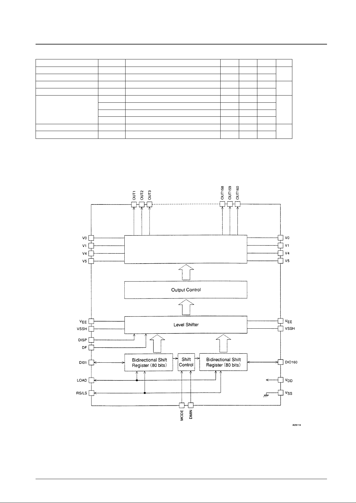
Overview
The LC4102C is a common driver for large-scale dot
matrix LCD panels. It includes a 160-bit bidirectional shift
register and 4-level LCD driver circuits. The number of
bits can be further increased by using the provided input
and output pins to connect multiple LC4102Cs in cascade.
The LC4102C and LC4104C form a large-screen LCD
panel driver chip set.
Features
• Fabricated in a CMOS (P-sub) high-voltage process.
• LCD drive voltage: 36 V
• Logic system power-supply voltage: 2.7 to 5.5 V
• fcp max: 2.5 MHz
• Slim chip (output pads are concentrated on one of the
longer sides)
• Bidirectional shift register
• The shift register can be split into two 80-bit registers.
(Two screens drivable)
• DISPOFF function that locks the drive voltages output
to the LCD at fixed levels.
• Display duty: 1/160 to 1/480
• Appropriate for COG (chip on glass) mounting. (A gold
bump structure is adopted in the pad areas.)
CMOS LSI
Ordering number : EN5789A
43098HA (OT)/82097HA (OT) No. 5789-1/8
SANYO Electric Co.,Ltd. Semiconductor Bussiness Headquarters
TOKYO OFFICE Tokyo Bldg., 1-10, 1 Chome, Ueno, Taito-ku, TOKYO, 110-8534 JAPAN
LCD Dot Matrix Common Driver
for STN Displays
LC4102C
Specifications
The electrical characteristics values shown below are for devices packaged in the Sanyo standard PGA-208 package.
Absolute Maximum Ratings at VSS= 0
Note: 1. LOAD, RS/LS, DISP, DF, DIO1, DIO160, DMIN and MODE
2. The voltages V0, V1, V4, and V5 must obey the relationships V
EE
≥ V0 ≥ V1 ≥ VEE– 7 V, and 7 V ≥ V4 ≥ V5 ≥ V
SSH
.
Allowable Operating Ranges at VSS= 0, Ta = –20 to +75°C
Note: 1. LOAD, RS/LS, DISP, DF, DIO1, DIO160, DMIN and MODE
2. The voltages V0, V1, V4, and V5 must obey the relationships V
EE
≥ V0 ≥ V1 ≥ VEE– 7 V, and 7 V ≥ V4 ≥ V5 ≥ V
SSH
.
When turning on the power supplies, first turn on the logic system power supply and then turn on the high-voltage system power supply; alternatively,
turn both on at the same time.
When turning off the power supplies, first turn off the high-voltage system power supply and then turn off the logic system power supply; alternatively,
turn both off at the same time.
Parameter Symbol Applicable pins min typ max Unit
V
DD
max V
DD
–0.3 7.0 V
Supply voltage V
EE
max V
EE
–0.3 40.0 V
V
SS
max V
SSH
–0.3 0.3 V
V
IN
*
1
–0.3 VDD+ 0.3 V
Input voltage
V0, V1 V0, V1 *
2
VEE– 7.0 VEE+ 0.3 V
V4 V4 *
2
–0.3 VSS+ 7.0 V
V5 V5 *
2
–0.3 +0.3 V
Operating temperature Topr –20 +75 °C
Storage temperature Tstg –55 +125 °C
Parameter Symbol Applicable pins min typ max Unit
V
DD
V
DD
2.7 5.5 V
Supply voltage V
EE
V
EE
14 36 V
V
SSH
V
SSH
0V
Input high-level voltage V
IH
*
1
0.8 × V
DD
V
DD
V
Input low-level voltage V
IL
*
1
0 0.2 × V
DD
V
V0, V1 V0, V1 *
2
VEE– 7.0 V
EE
V
Input voltage V4 V4 *
2
0
V
SSH
+ 7.0
V
V5 V5 *
2
0V
Electrical Characteristics at Ta = –20 to +75°C, VDD= 2.7 to 5.5 V, VSS= 0 V
Note: 1. LOAD, RS/LS, DISP, DF, DIO1, DIO160, DMIN and MODE
2. V
OUT
is the voltage applied by on-state outputs. V0 = VEE, V1 = 19/20 (VEE– V
SSH
), V4 = 1/20 (VEE– V
SSH
), V5 = V
SSH
, V
SSH
= V
SS
3. VDD= 2.7 to 5.5 V, fCP= 50 kHz
4. f
DF
= 100 Hz, with no output load, VEE= 36 V, for a single data shift
Block Diagram
No. 5789-2/8
LC4102C
Parameter Symbol Conditions min typ max Unit
Input high-level current I
IH
VIN= VDD*
1
1
µA
Input low-level current I
IL
VIN= VSS*
1
–1
Output high-level voltage V
OH
IOH= –0.4 mA, DIO1, DIO160
0.8 × V
DD
V
DD
V
Output low-level voltage V
OL
IOL= 0.4 mA, DIO1, DIO160 V
SS
0.2 × V
DD
RON0 V
OUT
= V0 – 0.5 V *2, OUT1 to 160 1000
Output on resistance
RON1 V
OUT
= V1 – 0.5 V *2, OUT1 to 160 1000
Ω
RON4 V
OUT
= V4 + 0.5 V *2, OUT1 to 160 1000
RON5 V
OUT
= V5 + 0.5 V *2, OUT1 to 160 1000
Current drain 1 I
DD
VDD*3 200
µA
Current drain 2 I
DDH
VDD*4 500
4-Level LCD Driver CIRCUIT (160 bits)

Switching Characteristics at VDD= 2.7 to 5.5 V, Ta = –20 to +75°C, VSS= 0 V
Switching Characteristics
No. 5789-3/8
LC4102C
Parameter Symbol Conditions min typ max Unit
Clock frequency fload LOAD 2.5 MHz
High-level clock pulse width twl LOAD 100
Input setup time tsu LOAD, DIOn 100
Input hold time th DMIN 30
LOAD falling time tr LOAD 30
ns
LOAD rising time tf LOAD 30
DIO output delay time tpld LOAD, DIOn: 30 pF capacitance load 200
LOAD-on delay time tplo LOAD, OUTn: 100 pF capacitance load 1.0
µs
DF-on delay time tpdfo DF, OUTn: 100 pF capacitance load 1.0
DIO output
Pin Functions
No. 5789-4/8
LC4102C
Symbol I/O Function
OUT1 to
OUT160
V0
V1
V4
V5
V
EE
V
SSH
DISP
DF
LOAD
MODE
RS/LS
DIO1
DMIN
DIO160
V
DD
V
SS
O
I
I
I
I
–
–
I
I
I
I
I
I/O
I
I/O
——Logic system power supply
Logic system ground
LCD drive outputs
V0 level drive voltage input
V1 level drive voltage input
V4 level drive voltage input
V5 level drive voltage input
High-voltage block power supply
High-voltage block ground
All outputs will be held at a fixed V5 level when this pin is low.
Alternation input
Data shift pulse input (falling edge)
Data shift direction specification input
*: don’t care
DF Data DISP OUTn
L H H V0
H L H V1
L L H V4
H H H V5
* * L V5
MODE RS/LS Shift direction DIO1 DIO160 DMIN
L L OUT160 →OUT1 OUT IN *
L H OUT1 →OUT160 IN OUT *
H L
OUT160 → OUT81
OUT IN IN
OUT80 → OUT1
H H
OUT1 → OUT80
IN OUT IN
OUT81 → OUT160
*: don’t care (Must be fixed at low or high.)
Note: * This IC is sensitive to ESD care must be used when handling this device.
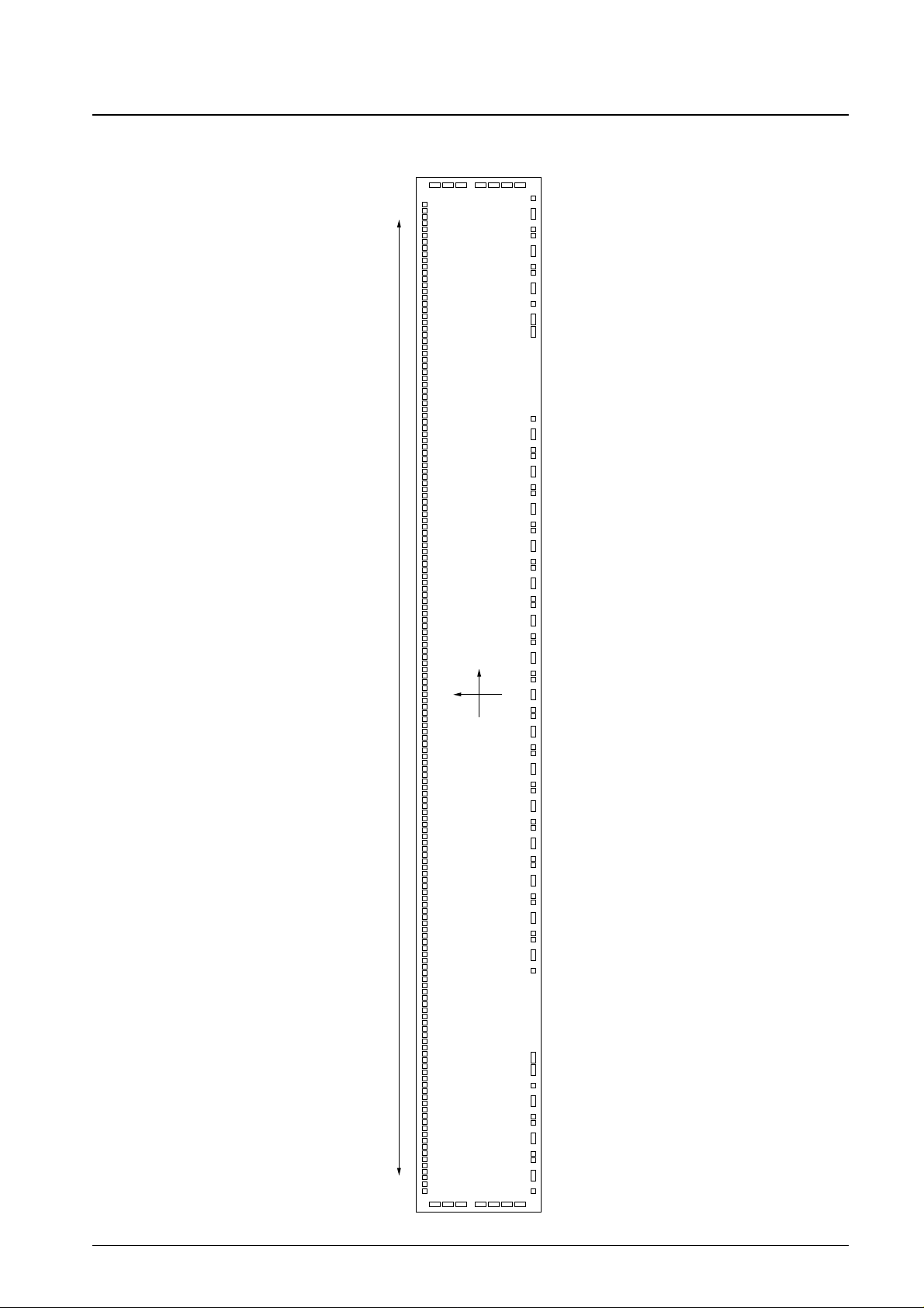
Pad Assignment
No. 5789-5/8
LC4102C
V4
V4
V4
V1
V1
V1
V0
V0
V0
NC
NC
VEE
VEE
VEE
VSSH
VSSH
VSSH
NC
DIO160
NC
NC
DMIN
NC
NC
DIO1
NC
VSS
VSS
VSS
NC
LOAD
NC
VSS
VSS
VSS
NC
DF
NC
NC
DISP
NC
VDD
VDD
VDD
NC
RSLS
NC
NC
MODE
NC
VSSH
VSSH
VSSH
VEE
VEE
VEE
NC
NC
V0
V0
V0
V1
V1
V1
V4
V4
V4
V5
V5
V5
V5
VSSH
VSSH
VSSH
OUT1
OUT2
OUT159
OUT160
V5
V5
V5
V5
VSSH
VSSH
VSSH
Chip size: 15.75 mm × 1.95 mm
X (+)
Y (+)
(0, 0)

LC4102C Pad Coordinates
No. 5789-6/8
LC4102C
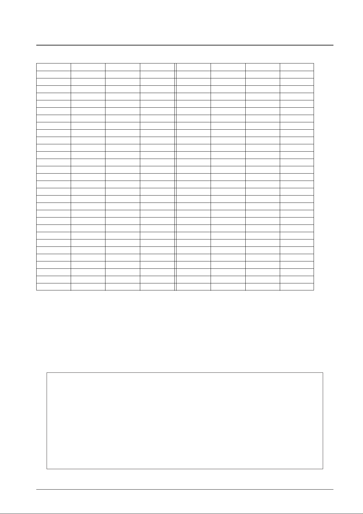
Pin X coordinate Y coordinate Pad type Pin X coordinate Y coordinate Pad type
V
SSH
–7708.4 349.5 A V
SS
250.0 –799.5 B
V
SSH
–7708.4 209.5 A NC 350.0 –799.5 B
V
SSH
–7708.4 69.5 A LOAD 600.0 –799.5 C
V5 –7708.4 –200.5 A NC 850.0 –784.5 B
V5 –7708.4 –340.5 A V
SS
950.0 –784.5 B
V5 –7708.4 –480.5 A V
SS
1200.0 –784.5 C
V5 –7708.4 –620.5 A V
SS
1450.0 –784.5 B
V4 –7570.0 –777.0 B NC 1550.0 –784.5 B
V4 –7320.0 –777.0 C DIO1 1800.0 –799.5 C
V4 –7070.0 –777.0 B NC 2050.0 –799.5 B
V1 –6850.0 –777.0 B NC 2150.0 –799.5 B
V1 –6600.0 –777.0 C DMIN 2400.0 –799.5 C
V1 –6350.0 –777.0 B NC 2650.0 –799.5 B
V0 –6250.0 –777.0 B NC 2750.0 –799.5 B
V0 –6000.0 –777.0 C DIO160 3000.0 –799.5 C
V0 –5750.0 –777.0 B NC 3250.0 –799.5 B
NC –5600.0 –764.5 A V
SSH
3350.0 –799.5 B
NC –5460.0 –764.5 A V
SSH
3600.0 –799.5 C
V
EE
–4450.0 –799.5 B V
SSH
3850.0 –799.5 B
V
EE
–4200.0 –799.5 C V
EE
3950.0 –799.5 B
V
EE
–3950.0 –799.5 B V
EE
4200.0 –799.5 C
V
SSH
–3850.0 –799.5 B V
EE
4450.0 –799.5 B
V
SSH
–3600.0 –799.5 C NC 5460.0 –779.5 A
V
SSH
–3350.0 –799.5 B NC 5600.0 –779.5 A
NC –3250.0 –799.5 B V0 5750.0 –779.5 B
MODE –3000.0 –799.5 C V0 6000.0 –779.5 C
NC –2750.0 –799.5 B V0 6250.0 –779.5 B
NC –2650.0 –799.5 B V1 6350.0 –779.5 B
RSLS –2400.0 –799.5 C V1 6600.0 –779.5 C
NC –2150.0 –799.5 B V1 6850.0 –779.5 B
V
DD
–2050.0 –799.5 B V4 7000.0 –779.5 B
V
DD
–1800.0 –799.5 C V4 7250.0 –779.5 C
V
DD
–1550.0 –799.5 B V4 7500.0 –779.5 B
NC –1450.0 –799.5 B V5 7708.4 –620.5 A
DISP –1200.0 –799.5 C V5 7708.4 –480.5 A
NC –950.0 –799.5 B V5 7708.4 –340.5 A
NC –850.0 –799.5 B V5 7708.4 –200.5 A
DF –600.0 –799.5 C V
SSH
7708.4 69.5 A
NC –350.0 –799.5 B V
SSH
7708.4 209.5 A
V
SS
–250.0 –799.5 B V
SSH
7708.4 349.5 A
V
SS
0.0 –799.5 C
Continued on next page.
Pad type Size
A 100 µm × 60 µm
B 60 µm × 60 µm
C 120 µm × 60 µm
D 75 µm × 60 µm
Continued from preceding page.
No. 5789-7/8
LC4102C
Pin X coordinate Y coordinate Pad type Pin X coordinate Y coordinate Pad type
OUT1 –7551.5 707.5 D OUT51 –2801.5 707.5 D
OUT2 –7456.5 707.5 D OUT52 –2706.5 707.5 D
OUT3 –7361.5 707.5 D OUT53 –2611.5 707.5 D
OUT4 –7266.5 707.5 D OUT54 –2516.5 707.5 D
OUT5 –7171.5 707.5 D OUT55 –2421.5 707.5 D
OUT6 –7076.5 707.5 D OUT56 –2326.5 707.5 D
OUT7 –6981.5 707.5 D OUT57 –2231.5 707.5 D
OUT8 –6886.5 707.5 D OUT58 –2136.5 707.5 D
OUT9 –6791.5 707.5 D OUT59 –2041.5 707.5 D
OUT10 –6696.5 707.5 D OUT60 –1946.5 707.5 D
OUT11 –6601.5 707.5 D OUT61 –1851.5 707.5 D
OUT12 –6506.5 707.5 D OUT62 –1756.5 707.5 D
OUT13 –6411.5 707.5 D OUT63 –1661.5 707.5 D
OUT14 –6316.5 707.5 D OUT64 –1566.5 707.5 D
OUT15 –6221.5 707.5 D OUT65 –1471.5 707.5 D
OUT16 –6126.5 707.5 D OUT66 –1376.5 707.5 D
OUT17 –6031.5 707.5 D OUT67 –1281.5 707.5 D
OUT18 –5936.5 707.5 D OUT68 –1186.5 707.5 D
OUT19 –5841.5 707.5 D OUT69 –1091.5 707.5 D
OUT20 –5746.5 707.5 D OUT70 –996.5 707.5 D
OUT21 –5651.5 707.5 D OUT71 –901.5 707.5 D
OUT22 –5556.5 707.5 D OUT72 –806.5 707.5 D
OUT23 –5461.5 707.5 D OUT73 –711.5 707.5 D
OUT24 –5366.5 707.5 D OUT74 –616.5 707.5 D
OUT25 –5271.5 707.5 D OUT75 –521.5 707.5 D
OUT26 –5176.5 707.5 D OUT76 –426.5 707.5 D
OUT27 –5081.5 707.5 D OUT77 –331.5 707.5 D
OUT28 –4986.5 707.5 D OUT78 –236.5 707.5 D
OUT29 –4891.5 707.5 D OUT79 –141.5 707.5 D
OUT30 –4796.5 707.5 D OUT80 –46.5 707.5 D
OUT31 –4701.5 707.5 D OUT81 48.5 707.5 D
OUT32 –4606.5 707.5 D OUT82 143.5 707.5 D
OUT33 –4511.5 707.5 D OUT83 238.5 707.5 D
OUT34 –4416.5 707.5 D OUT84 333.5 707.5 D
OUT35 –4321.5 707.5 D OUT85 428.5 707.5 D
OUT36 –4226.5 707.5 D OUT86 523.5 707.5 D
OUT37 –4131.5 707.5 D OUT87 618.5 707.5 D
OUT38 –4036.5 707.5 D OUT88 713.5 707.5 D
OUT39 –3941.5 707.5 D OUT89 808.5 707.5 D
OUT40 –3846.5 707.5 D OUT90 903.5 707.5 D
OUT41 –3751.5 707.5 D OUT91 998.5 707.5 D
OUT42 –3656.5 707.5 D OUT92 1093.5 707.5 D
OUT43 –3561.5 707.5 D OUT93 1188.5 707.5 D
OUT44 –3466.5 707.5 D OUT94 1283.5 707.5 D
OUT45 –3371.5 707.5 D OUT95 1378.5 707.5 D
OUT46 –3276.5 707.5 D OUT96 1473.5 707.5 D
OUT47 –3181.5 707.5 D OUT97 1568.5 707.5 D
OUT48 –3086.5 707.5 D OUT98 1663.5 707.5 D
OUT49 –2991.5 707.5 D OUT99 1758.5 707.5 D
OUT50 –2896.5 707.5 D OUT100 1853.5 707.5 D
Continued on next page.
PS. No. 5789-8/8
LC4102C
Continued from preceding page.
Pin X coordinate Y coordinate Pad type Pin X coordinate Y coordinate Pad type
OUT101 1948.5 707.5 D OUT131 4798.5 707.5 D
OUT102 2043.5 707.5 D OUT132 4893.5 707.5 D
OUT103 2138.5 707.5 D OUT133 4988.5 707.5 D
OUT104 2233.5 707.5 D OUT134 5083.5 707.5 D
OUT105 2328.5 707.5 D OUT135 5178.5 707.5 D
OUT106 2423.5 707.5 D OUT136 5273.5 707.5 D
OUT107 2518.5 707.5 D OUT137 5368.5 707.5 D
OUT108 2613.5 707.5 D OUT138 5463.5 707.5 D
OUT109 2708.5 707.5 D OUT139 5558.5 707.5 D
OUT110 2803.5 707.5 D OUT140 5653.5 707.5 D
OUT111 2898.5 707.5 D OUT141 5748.5 707.5 D
OUT112 2993.5 707.5 D OUT142 5843.5 707.5 D
OUT113 3088.5 707.5 D OUT143 5938.5 707.5 D
OUT114 3183.5 707.5 D OUT144 6033.5 707.5 D
OUT115 3278.5 707.5 D OUT145 6128.5 707.5 D
OUT116 3373.5 707.5 D OUT146 6223.5 707.5 D
OUT117 3468.5 707.5 D OUT147 6318.5 707.5 D
OUT118 3563.5 707.5 D OUT148 6413.5 707.5 D
OUT119 3658.5 707.5 D OUT149 6508.5 707.5 D
OUT120 3753.5 707.5 D OUT150 6603.5 707.5 D
OUT121 3848.5 707.5 D OUT151 6698.5 707.5 D
OUT122 3943.5 707.5 D OUT152 6793.5 707.5 D
OUT123 4038.5 707.5 D OUT153 6888.5 707.5 D
OUT124 4133.5 707.5 D OUT154 6983.5 707.5 D
OUT125 4228.5 707.5 D OUT155 7078.5 707.5 D
OUT126 4323.5 707.5 D OUT156 7173.5 707.5 D
OUT127 4418.5 707.5 D OUT157 7268.5 707.5 D
OUT128 4513.5 707.5 D OUT158 7363.5 707.5 D
OUT129 4608.5 707.5 D OUT159 7458.5 707.5 D
OUT130 4703.5 707.5 D OUT160 7553.5 707.5 D
This catalog provides information as of April, 1998. Specifications and information herein are subject to change
without notice.
■ No products described or contained herein are intended for use in surgical implants, life-support systems, aerospace
equipment, nuclear power control systems, vehicles, disaster/crime-prevention equipment and the like, the failure of
which may directly or indirectly cause injury, death or property loss.
■ Anyone purchasing any products described or contained herein for an above-mentioned use shall:
➀ Accept full responsibility and indemnify and defend SANYO ELECTRIC CO., LTD., its affiliates, subsidiaries and
distributors and all their officers and employees, jointly and severally, against any and all claims and litigation and all
damages, cost and expenses associated with such use:
➁ Not impose any responsibility for any fault or negligence which may be cited in any such claim or litigation on
SANYO ELECTRIC CO., LTD., its affiliates, subsidiaries and distributors or any of their officers and employees
jointly or severally.
■ Information (including circuit diagrams and circuit parameters) herein is for example only; it is not guaranteed for
volume production. SANYO believes information herein is accurate and reliable, but no guarantees are made or implied
regarding its use or any infringements of intellectual property rights or other rights of third parties.
 Loading...