

Page 1
Overview
The LC3564B, LC3564BS, LC3564BM, and LC3564BT
are 8192-word × 8-bit asynchronous silicon gate CMOS
SRAMs. These are full CMOS type SRAMs that adopt a
six-transistor memory cell and feature fast access times,
low operating power dissipation, and an ultralow standby
current. These SRAMs provide three control signal inputs:
an OE input for high-speed memory access, and two chip
enable lines, CE1 and CE2, for low power mode and
device selection. These means that these SRAMs area
ideal for systems that require low power and battery
backup, and that they support easy memory expansion.
The ultralow standby current that is a feature of these
SRAMs allows them to be used with capacitor backup as
well. Since these SRAMs support 3-V operation, they are
also appropriate for use in portable battery operated
systems.
Features
• Supply voltage range: 2.7 to 5.5 V
— In 5-V operation mode: 5.0 V ±10%
— In 3-V operation mode: 3.0 V ±10%
• Address access time (tAA)
— In 5-V operation mode:
LC3564B, BS, BM, and BT-70: 70 ns (max)
LC3564B, BS, BM, and BT-10: 100 ns (max)
— In 3-V operation mode:
LC3564B, BS, BM, and BT-70: 200 ns (max)
LC3564B, BS, BM, and BT-10: 500 ns (max)
• Ultralow standby current
— In 5-V operation mode: 1.0 µA (Ta ≤ 70°C),
3.0 µA (Ta ≤ 85°C)
— In 3-V operation mode: 0.8 µA (Ta ≤ 70°C),
2.5 µA (Ta ≤ 85°C)
• Operating temperature range
— In 5-V operation mode: –40 to 85°C
— In 3-V operation mode: –40 to 85°C
• Data retention supply voltage: 2.0 to 5.5 V
• All input and output levels:
— In 5-V operation mode: TTL compatible levels
— In 3-V operation mode: V
CC
–0.2 V/0.2 V
• Three control inputs: OE, CE1, and CE2
• Shared input and output pins, three-state outputs
• No clock required
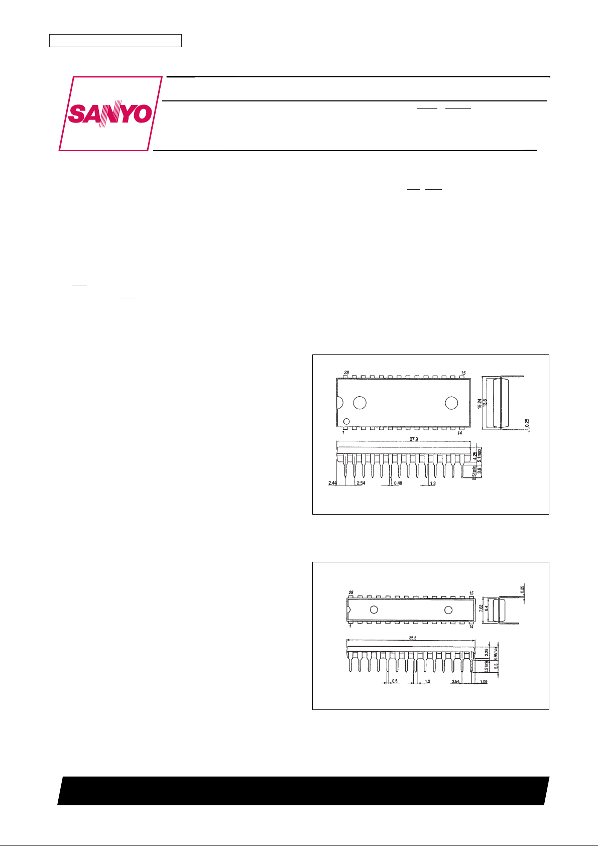
• Packages
28-pin DIP (600 mil) plastic package: LC3564B
28-pin DIP (300 mil) plastic package: LC3564BS
28-pin SOP (450 mil) plastic package: LC3564BM
28-pin TSOP (8 × 13.4 mm) plastic package: LC3564BT
Package Dimensions
unit: mm
3012A-DIP28 (600 mil)
unit: mm
3133-DIP28 (300 mil)
CMOS IC
53098HA (OT) No. 5804-1/9
SANYO: DIP28 (600 mil)
[LC3564B]
SANYO: DIP28 (300 mil)
[LC3564BS]
SANYO Electric Co.,Ltd. Semiconductor Bussiness Headquarters
TOKYO OFFICE Tokyo Bldg., 1-10, 1 Chome, Ueno, Taito-ku, TOKYO, 110-8534 JAPAN
64K (8192-word × 8-bit) SRAM with OE, CE1, and CE2
Control Pins
LC3564B, BS, BM, BT-70/10
Ordering number : EN5804A
Page 2
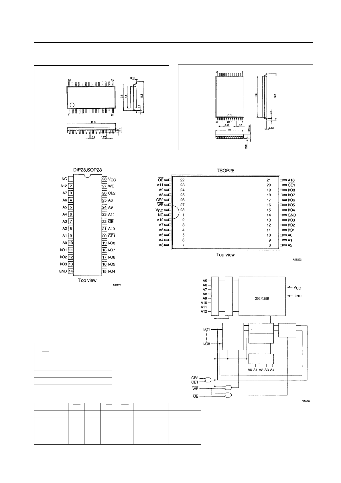
No. 5804-2/9
LC3564B, BS, BM, BT-70/10
SANYO: SOP28
[LC3564BM]
unit: mm
3187-SOP28
Pin Assignments
SANYO: TSOP28 (type I)
[LC3564BT]
unit: mm
3221-TSOP28 (type I)
Block Diagram
Pin Functions
A0 to A12 Address inputs
WE Read/write control input
OE Output enable input
CE1, CE2 Chip enable inputs
I/O1 to I/O8 Data I/O
V
CC
, GND Power supply and ground
Function Table
X : H or L
Mode CE1 CE2 OE WE I/O Supply current
Read cycle L H L H Data output I
CCA
Write cycle L H X L Data input I
CCA
Output disable L H H H High impedance I
CCA
Not selected
H X X X High impedance I
CCS
X L X X High impedance I
CCS
Address buffer
Input data
buffer
Input data
control circuit
Row decoder
Memory cell array
Column
I/O circuit
Column
decoder
Address
buffer
Output
data
Page 3
No. 5804-3/9
LC3564B, BS, BM, BT-70/10
Parameter Symbol Conditions Ratings Unit
Maximum supply voltage V
CC
max 7.0 V
Input voltage V
IN
–0.3* to VCC+ 0.3 V
I/O voltage V
I/O
–0.3 to VCC+ 0.3 V
Operating temperature Topr –40 to +85 °C
Storage temperature Tstg –55 to +125 °C
Specifications
Absolute Maximum Ratings at Ta = 25°C
Note: For pulse widths less than 30 ns: –3.0 V
Note: These parameters are sampled, and are not measured for every unit.
Note: For pulse widths less than 30 ns: –3.0 V
Note *: Reference values at V
CC
= 5 V, Ta = 25°C
[5-V Operation]
Parameter Symbol Conditions
Ratings
Unit
min typ max
I/O pin capacitance C
I/OVI/O
= 0 V 6 10 pF
Input pin capacitance C
IN
VIN= 0 V 6 10 pF
Input and Output Capacitances at Ta = 25°C, f = 1 MHz
Parameter Symbol Conditions
Ratings
Unit
min typ max
Supply voltage V
CC
4.5 5.0 5.5 V
Input voltage
V
IH
2.2 VCC+ 0.3 V
V
IL
–0.3* +0.8 V
DC Allowable Operating Ranges at Ta = –40 to +85°C, VCC= 4.5 to 5.5 V
Parameter Symbol Conditions
Ratings
Unit
min typ * max
Input leakage current I
LI
VIN= 0 to V
CC
–1.0 +1.0 µA
I/O leakage current I
LO
V
CE1
= VIHor V
CE2
= VILor VOE= VIHor
–1.0 +1.0 µA
V
WE
= VIL, V
I/O
= 0 to V
CC
Output high-level voltage V
OHIOH
= –1.0 mA 2.4 V
Output low-level voltage V
OLIOL
= 2.0 mA 0.4 V
V
CE1
≤ 0.2 V, V
CE2
≥ VCC– 0.2 V,
Ta ≤ 70°C
0.01 1.0 µA
I
CCA1II/O
= 0 mA, VIN≤ 0.2 V or
VCC– 0.2 V/0.2 V
V
IN
≥ VCC– 0.2 V
Ta ≤ 85°C
3.0
inputs
min
LC3564B,BS, BM, BT-70
35
mA
I
CCA4
cycle
LC3564B,BS,BM,BT-10
30
1 µs cycle 4 mA
Operating supply current
I
CCA2
V
CE1
= VIL, V
CE2
= VIH, I
I/O
= 0 mA,
7 mA
V
IN
= VIHor V
IL
TTL inputs min
LC3564B,BS, BM, BT-70
40
mA
I
CCA3
cycle
LC3564B,BS,BM,BT-10
35
1 µs cycle 7 mA
Standby mode supply
V
CC
– 0.2 V/0.2 V
V
CE2
≤ 0.2 V or
Ta ≤ 70°C
0.01 1.0
µA
current
inputs
I
CCS1VCE1
≥ VCC– 0.2 V
V
CE2
≥ VCC– 0.2 V
Ta ≤ 85°C
3.0
TTL inputs I
CC2VCE2
= VILor V
CE1
= VIH, VIN= 0 to V
CC
2.0 mA
DC Electrical Characteristics at Ta = –40 to +85°C, VCC= 4.5 to 5.5 V
V
CE1
≤ 0.2 V,
V
CE2
≥ VCC– 0.2 V,
I
I/O
= 0 mA,
DUTY = 100%
V
CE1
= VIL,
V
CE2
= VIH,
I
I/O
= 0 mA,
DUTY = 100%
Page 4

AC Electrical Characteristics at Ta = –40 to +85°C, VCC= 4.5 to 5.5 V
No. 5804-4/9
LC3564B, BS, BM, BT-70/10
LC3564B, BS, BM, BT
Parameter Symbol -70 -10 Unit
min max min max
Read cycle time t
RC
70 100 ns
Address access time t
AA
70 100 ns
CE1 access time t
CA1
70 100 ns
CE2 access time t
CA2
70 100 ns
OE access time t
OA
35 50 ns
Output hold time t
OH
10 10 ns
CE1 output enable time t
COE1
10 10 ns
CE2 output enable time t
COE2
10 10 ns
OE output enable time t
OOE
5 5 ns
CE1 output disable time t
COD1
30 35 ns
CE2 output disable time t
COD2
30 35 ns
OE output disable time t
OOD
25 25 ns
Read Cycle
LC3564B, BS, BM, BT
Parameter Symbol -70 -10 Unit
min max min max
Write cycle time t
WC
70 100 ns
Address setup time t
AS
0 0 ns
Write pulse width t
WP
50 55 ns
CE1 setup time t
CW1
60 65 ns
CE2 setup time t
CW2
60 65 ns
Write recovery time t
WR
0 0 ns
CE1 write recovery time t
WR1
0 0 ns
CE2 write recovery time t
WR2
0 0 ns
Data setup time t
DS
35 40 ns
Data hold time t
DH
0 0 ns
CE1 data hold time t
DH1
0 0 ns
CE2 data hold time t
DH2
0 0 ns
WE output enable time t
WOE
5 5 ns
WE output disable time t
WOD
30 35 ns
Write Cycle
Parameter Conditions
[AC Test Conditions]
Input pulse voltage V
IH
= 2.4 V, VIL= 0.6 V
Input rise and fall times 5 ns
Input and output timing level 1.5 V
Output load
LC3564B, BS, BM, and BT-70: 30 pF + 1 TTL gate (Including the jig capacitance.)
LC3564B, BS, BM, and BT-10: 100 pF + 1 TTL gate (Including the jig capacitance.)
Page 5

[3-V Operation]
No. 5804-5/9
LC3564B, BS, BM, BT-70/10
Note *: Reference values at VCC= 3 V, Ta = 25°C
Parameter Symbol Conditions
Ratings
Unit
min typ max
Supply voltage V
CC
2.7 3.0 3.3 V
Input voltage
V
IH
VCC– 0.2 V
CC
V
V
IL
0 0.2 V
DC Allowable Operating Ranges at Ta = –40 to +85°C, VCC= 2.7 to 3.3 V
Parameter Symbol Conditions
Ratings
Unit
min typ * max
Input leakage current I
LI
VIN= 0 to V
CC
–1.0 +1.0 µA
I/O leakage current I
LO
V
CE1
= VIHor V
CE2
= VILor VOE= VIHor
–1.0 +1.0 µA
V
WE
= VIL, V
I/O
= 0 to V
CC
Output high-level voltage V
OHIOH
= –0.5 mA VCC– 0.2 V
Output low-level voltage V
OLIOL
= 1.0 mA 0.2 V
V
CE1
≤ VIL, V
CE2
≥ VIH,
Ta ≤ 70°C
0.01 0.8
µAI
CCA1II/O
= 0 mA, VIN≤ VILor
V
IN
≥ V
IH
Ta ≤ 85°C
2.5
Operation supply current
V
CC
– 0.2 V/0.2 V
min
LC3564B,BS, BM, BT-70
20
mA
inputs
I
CCA4
cycle
LC3564B,BS,BM,BT-10
10
1 µs cycle 3 mA
Standby mode supply V
CC
– 0.2 V/0.2 V
V
CE2
≤ 0.2 V or
Ta ≤ 70°C
0.01 0.8
µA
current inputs
I
CCS1VCE1
≥ V
IH
V
CE2
≥ V
IH
Ta ≤ 85°C
2.5
DC Electrical Characteristics at Ta = –40 to +85°C, VCC= 2.7 to 3.3 V
V
CE1
≤ VIL,
V
CE2
≥ VIH,
I
I/O
= 0 mA,
DUTY = 100%
Page 6

No. 5804-6/9
LC3564B, BS, BM, BT-70/10
AC Electrical Characteristics at Ta = –40 to +85°C, VCC= 2.7 to 3.3 V
LC3564B, BS, BM, BT
Parameter Symbol -70 -10 Unit
min max min max
Read cycle time t
RC
200 500 ns
Address access time t
AA
200 500 ns
CE1 access time t
CA1
200 500 ns
CE2 access time t
CA2
200 500 ns
OE access time t
OA
100 250 ns
Output hold time t
OH
20 20 ns
CE1 output enable time t
COE1
20 20 ns
CE2 output enable time t
COE2
20 20 ns
OE output enable time t
OOE
10 10 ns
CE1 output disable time t
COD1
60 120 ns
CE2 output disable time t
COD2
60 120 ns
OE output disable time t
OOD
50 100 ns
Read Cycle
LC3564B, BS, BM, BT
Parameter Symbol -70 -10 Unit
min max min max
Write cycle time t
WC
200 500 ns
Address setup time t
AS
0 0 ns
Write pulse width t
WP
140 200 ns
CE1 setup time t
CW1
150 250 ns
CE2 setup time t
CW2
0 250 ns
Write recovery time t
WR
0 0 ns
CE1 write recovery time t
WR1
0 0 ns
CE2 write recovery time t
WR2
130 0 ns
Data setup time t
DS
0 180 ns
Data hold time t
DH
0 0 ns
CE1 data hold time t
DH1
0 0 ns
CE2 data hold time t
DH2
10 0 ns
WE output enable time t
WOE
10 ns
WE output disable time t
WOD
60 120 ns
Write Cycle
Parameter Conditions
[AC Test Conditions]
Input pulse voltage V
IH
= VCC– 0.2 V, VIL= 0.2 V
Input rise and fall times 10 ns
Input and output timing level 1.5 V
Output load
LC3564B, BS, BM, BT-70 : 30pF (Including the jig capacitance.)
LC3564B, BS, BM, BT-10 : 100pF (Including the jig capacitance.)
Page 7

Timing Charts
Read Cycle *1
Write Cycle (1): WE Write *6
No. 5804-7/9
LC3564B, BS, BM, BT-70/10
Page 8

No. 5804-8/9
LC3564B, BS, BM, BT-70/10
Write Cycle (2): CE1 Write *6
Write Cycle (3): CE2 Write *6
Notes: 1. Hold WE high during the read cycle.
2. Applications must not apply reverse phase signals to the D
OUT
pins when those pins are in the output state.
3. The time tWP is the period when CE1 and WE are low and CE2 is high, and is defined as the time from the fall of WE until either CE1 or WE rises,
or CE2 falls, whichever occurs first.
4. The times t
CW1
and t
CW2
are periods when CE1 and WE are low and CE2 is high. They are defined as the times from the fall of CE1 or the rise of
CE2 to the rise of CE1 and WE, or the fall of CE2, whichever occurs first.
5. The D
OUT
pins will be in the high-impedance state if either OE is high, CE1 is high, CE2 is low, or WE is low.
6. OE must be held either at V
IH
or VILduring the write cycle.
7. The D
OUT
pins have the same phase as the write cycle write data.
Page 9

PS No. 5804-9/9
LC3564B, BS, BM, BT-70/10
This catalog provides information as of May, 1998. Specifications and information herein are subject to change
without notice.
■ No products described or contained herein are intended for use in surgical implants, life-support systems, aerospace
equipment, nuclear power control systems, vehicles, disaster/crime-prevention equipment and the like, the failure of
which may directly or indirectly cause injury, death or property loss.
■ Anyone purchasing any products described or contained herein for an above-mentioned use shall:
➀ Accept full responsibility and indemnify and defend SANYO ELECTRIC CO., LTD., its affiliates, subsidiaries and
distributors and all their officers and employees, jointly and severally, against any and all claims and litigation and all
damages, cost and expenses associated with such use:
➁ Not impose any responsibility for any fault or negligence which may be cited in any such claim or litigation on
SANYO ELECTRIC CO., LTD., its affiliates, subsidiaries and distributors or any of their officers and employees
jointly or severally.
■ Information (including circuit diagrams and circuit parameters) herein is for example only; it is not guaranteed for
volume production. SANYO believes information herein is accurate and reliable, but no guarantees are made or implied
regarding its use or any infringements of intellectual property rights or other rights of third parties.
Parameter Symbol Conditions
Ratings
Unit
min typ max
Data retention supply voltage
V
DR
V
CE2
≤ 0.2 V or
2.0 5.5 µA
V
CE1
≥ VCC– 0.2 V, V
CE2
≥ VCC– 0.2 V
V
CC
= 3V, V
CE2
≤ 0.2 V,
Ta ≤ 70°C
0.8
µA
Data retention supply current I
CCDR
or V
CE1
≥ VCC– 0.2 V,
V
CE2
≥ VCC– 0.2 V
Ta ≤ 85°C
2.5
Chip enable setup time t
CDR
0 ns
Chip enable hold time t
R
tRC* ns
Data Retention Characteristics at Ta = –40 to +85°C
Note *: tRCis the read cycle time.
Note *:In 5-V operation: 4.5 V
In 3-V operation: 2.7 V
Data retention mode
Data Retention Waveforms (1): CE1 Control
Notes on Circuit Design
When actually design a circuit using these devices, take the following points into consideration and design the circuit so
that none of the maximum rating items are ever exceeded.
• Variations in the supply voltage
• Variations in the electrical characteristics of components such as semiconductor devices, resistors, and capacitors.
• Ambient temperature
• Variations in input and clock signals
• Possible application of abnormal pulses
Also, these devices must be operated within the ranges stipulated in the allowable operating ranges.
If CMOS IC input pins are left open, intermediate potential input voltages may occur leading to incorrect operation due
to through currents or other phenomenon. Applications must handle unused input pins appropriately.
Data Retention Waveforms (2): CE2 Control
Data retention mode
 Loading...