

Ordering number : EN4430C
22897HA (OT)/52595TH (OT)/N1993JN/40893JN A8-9957, 58, 59, No. 4430-1/9
Overview
The LC33832 series is composed of pseudo static RAM
that operates on a single 5 V power supply and is
organized as 32768 words × 8 bits. By using memory
cells each composed of a single transistor and capacitor,
together with peripheral CMOS circuitry, this series
achieves ease of use with high density, high speed, and
low power dissipation. The LC33832 series can easily
accomplish auto-refresh and self-refresh by means of
OE/RFSH input. As with asynchronous static RAM, WE
input uses a system for incorporating input data at the WE
rise, thereby facilitating interfacing with a microcomputer.
The LC33832 series features pin compatibility with 256 K
static RAM (the LC36256A series), and available
packages are the standard 28-pin DIP with widths of 600
mil or 300 mil, and the SOP with a width of 450 mil.
CE-only refresh can be accomplished by selecting address
256 (A0 to A7) within 4 ms.
Features
• 32768 words × 8 bits configuration
• Single 5 V ±10% power supply
• All input and output (I/O) TTL compatible
• Fast access times and low power dissipation
• 4 ms refresh using 256 refresh cycle
• CE-only refresh, auto-refresh, and self-refresh
• Low-power version: 100 µA self-refresh current
• Package
DIP28-pin (600 mil) plastic package: LC33832P, PL
DIP28-pin (300 mil) plastic package: LC33832S, SL
SOP28-pin (450 mil) plastic package: LC33832M, ML
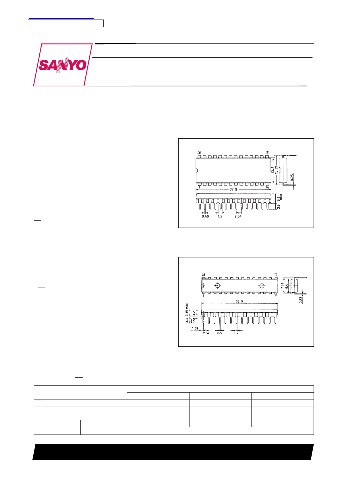
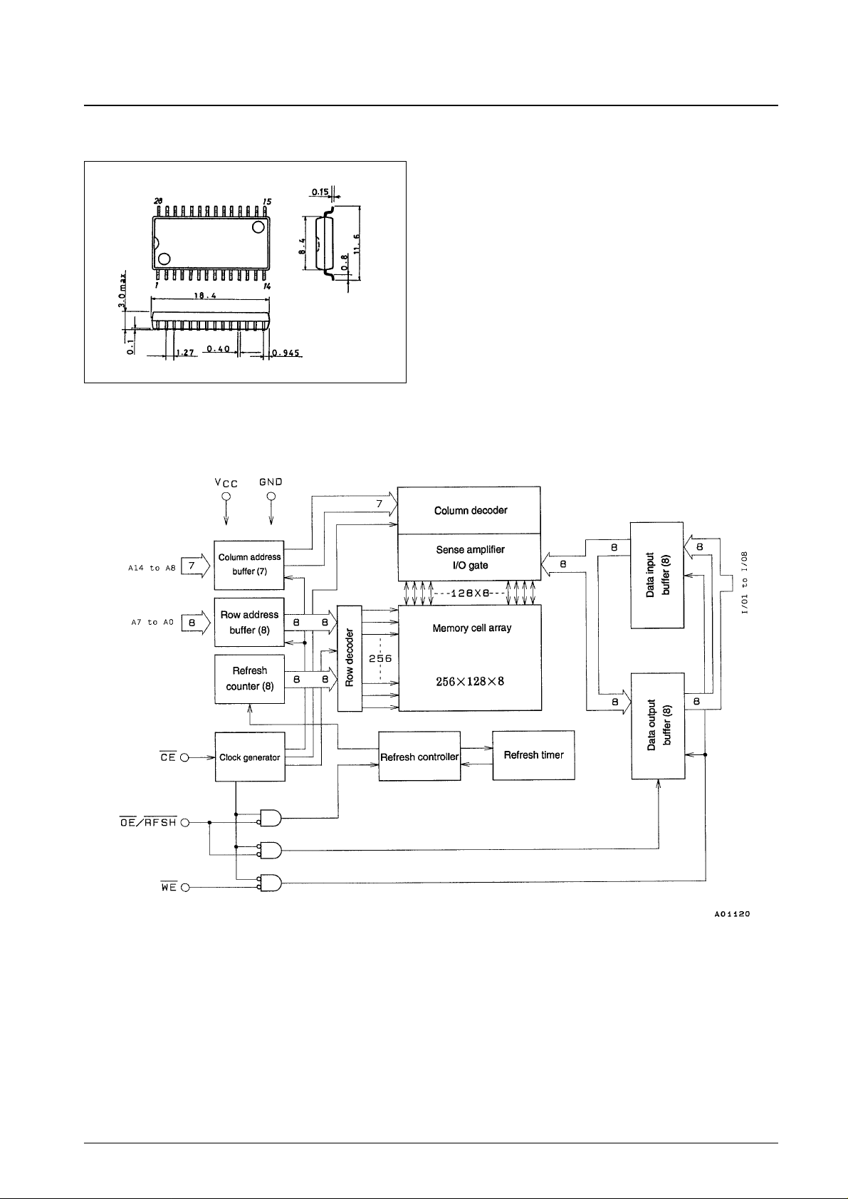
Package Dimensions
unit: mm
3012A-DIP28
unit: mm
3133-DIP28
SANYO: DIP28
[LC33832P, PL]
SANYO: DIP28
[LC33832S, SL]
LC33832P, S, M, PL, SL, ML-70/80/10
SANYO Electric Co.,Ltd. Semiconductor Bussiness Headquarters
TOKYO OFFICE Tokyo Bldg., 1-10, 1 Chome, Ueno, Taito-ku, TOKYO, 110-8534 JAPAN
256 K (32768 words × 8 bits) Pseudo-SRAM
CMOS LSI
Parameter
LC33832P, S, M, PL, SL, ML
-70 -80 -10
CE access time 70 ns 80 ns 100 ns
OE access time 30 ns 35 ns 40 ns
Cycle time 115 ns 130 ns 160 ns
Current drain
Operating 65 mA 60 mA 50 mA
Standby 1 mA/100 µA (L version)
• CE access time/OE access time/Cycle time/Current drain
查询LC33832M供应商
LC33832P, S, M, PL, SL, ML-70/80/10
No. 4430-2/9
Block Diagram
unit : mm
3158-SOP28
[LC33832M, ML]
SANYO: SOP28
LC33832P, S, M, PL, SL, ML-70/80/10
No. 4430-3/9
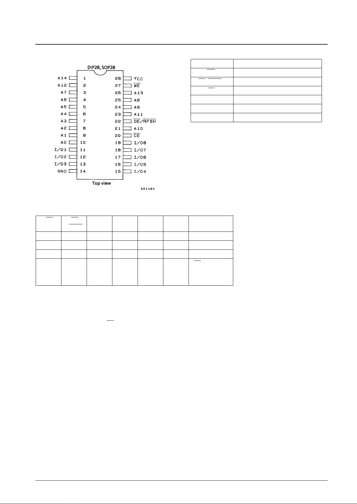
Pin Assignment Pin Functions
A0 to A14 Address input
WE Read/Write input
OE/RFSH Output-enable input/ refresh input
CE Chip-enable input
I/O1 to I/O8 Data input/output
V
CC
Power supply
GND Ground
Functional Logic
CE OE WE A0 to A7 A8 to I/O1 State
/RFSH A14 to I/O8
H H X X X HZ Standby
L L H VX VX OUT Read
L H L VX VX IN Write
L H H VX X HZ CE-only refresh
H L X X X HZ Self-refresh
H NP X X X HZ Auto-refresh
H...................High-level input of VIN= 6.5 V to VIH(min)
L....................Low-level input of VIN= VIL(max) to –1.0 V
X....................High- or low-level input
NP.................Negative-polarity pulse input
VX.................“IN” when CE = L is confirmed, then “X”
HZ.................High impedance
IN..................Input state
OUT..............Output state

LC33832P, S, M, PL, SL, ML-70/80/10
No. 4430-4/9
Specifications
Absolute Maximum Ratings
Parameter Symbol Ratings Unit Note
Maximum supply voltage V
CC
max –1.0 to +7.0 V 1
Input voltage V
IN
–1.0 to +7.0 V 1
Output voltage V
OUT
–1.0 to +7.0 V 1
Allowable power dissipation Pd max 600 mW 1
Output short-circuit current I
OUT
50 mA 1
Operating temperature Topr 0 to +70 °C 1
Storage temperature Tstg –55 to +150 °C 1
Note: 1) Stresses greater than the above listed maximum values may result in damage to the device.
DC Recommended Operating Ranges at Ta = 0 to +70°C
Parameter Symbol min typ max Unit Note
Supply voltage V
CC
4.5 5.0 5.5 V 2
Input high level voltage V
IH
2.4 6.5 V 2
Input low level voltage V
IL
–1.0 +0.8 V 2
Note: 2) All voltages are referenced to GND.
DC Electrical Characteristics at Ta = 0 to +70°C, VCC= 5V±10%
Parameter Symbol Conditions min max Unit Note
Operating current I
CCA
Average current during operation
70ns 65
Access 80ns 60 mA 3,4
time
100ns 50
Standby current 1 I
CCS1
CE = OE/RFSH = V
IH
1 mA
Standby current 2 I
CCS2
CE = OE/RFSH = VCC–0.2V
LC33832P, S, M 1 mA
LC33832PL, SL, ML 100 µA
Self-refresh current I
CCSR
CE = VCC–0.2V, OE/RFSH = 0.2V
LC33832P, S, M 1 mA
LC33832PL, SL, ML 100 µA
Input leakage current I
IL
0V≤VIN≤VCC, pins other than test pin = 0V –10 +10 µA
Output leakage current I
OL
D
OUT
disable, 0V≤V
OUT≤VCC
–10 +10 µA
Output high level voltage V
OHIOUT
= –5mA 2.4 V
Output low level voltage V
OLIOUT
= 4.2mA 0.4 V
Note: 3) All current values are measured at minimal cycle rate. Since current flows immoderately, cycle times may become longer
and shorter than shown here.
4) Dependent on output load. Maximum value is value during free state.
Input/Output Capacitance Characteristics at Ta = 25°C, f = 1MHz, VCC= 5V±10%
Parameter Symbol min max Unit Test conditions
Input capacitance (A0 to A14) C
IN1
5 pF V
IN1
= 0 V
Input capacitance (CE, OE/RFSH, WE) C
IN2
7 pF V
IN2
= 0 V
Input/output capacitance C
I/O
10 pF V
I/O
= 0 V
Sampling inspections, and not full-lot inspections, are carried out for these parameters.

LC33832P, S, M, PL, SL, ML-70/80/10
No. 4430-5/9
AC Electrical Characteristics at Ta = 0 to +70°C, VCC5V±10% (Notes 5, 6, 7, 8, 9)
LC33832P, S, M, PL, SL, ML
Parameter Symbol -70 -80 -10 Unit Note
min max min max min max
Random read, t
RC
115 130 160 ns
write cycle time
Read-write cycle time t
RMW
165 195 240 ns
CE pulse width t
CE
70 10000 80 10000 100 10000 ns
CE precharge time t
P
35 40 50 ns
CE access time t
CEA
70 80 100 ns
OE access time t
OEA
30 35 40 ns
CE output enable time t
CLZ
10 10 10 ns
OE output enable time t
OLZ
0 0 0 ns
WE output enable time t
WLZ
0 0 0 ns
CE output disable time t
CHZ
0 20 0 25 0 30 ns 10
OE output disable time t
OHZ
0 20 0 25 0 30 ns 10
WE output disable time t
WHZ
0 20 0 25 0 30 ns 10
OE hold time for CE t
OHC
0 0 0 ns
OE setup time for CE t
OSC
10 10 10 ns
Read command setup time t
RCS
0 0 0 ns
Read command hold time t
RCH
0 0 0 ns
Write pulse width t
WP
55 60 70 ns
Write command hold time t
WCH
55 60 70 ns
Write command lead time t
CWL
55 60 70 ns
Input data setup time for WE t
DSW
30 35 40 ns 11
Input data setup time for CE t
DSC
30 35 40 ns 11
Input data hold time for WE t
DHW
0 0 0 ns 11
Input data hold time for CE t
DHC
0 0 0 ns 11
Address setup time for CE t
ASC
0 0 0 ns 12
Address hold time for CE t
AHC
15 20 25 ns 12
Auto-refresh cycle time t
FC
115 130 160 ns
RFSH delay time for CE t
RFD
35 40 50 ns
RFSH pulse width (auto-refresh)
t
FAP
75 8000 80 8000 80 8000 ns 13
RFSH precharge time t
FP
30 30 30 ns 13
(auto-refresh)
RFSH active CE delay time t
FCE
135 160 190 ns 13
(auto-refresh)
RFSH pulse width (self-refresh) t
FAS
8000 8000 8000 ns 13
RFSH precharge CE delay time t
FRS
135 160 190 ns 13
(self-refresh)
Refresh time t
REF
4 4 4 ms
Rise and fall time t
T
3 50 3 50 3 50 ns
Continued on next page.

LC33832P, S, M, PL, SL, ML-70/80/10
No. 4430-6/9
Continued from preceding page.
Note : 5) To accomplish internal initialization, CE and OE/RFSH are fixed at VIHfor an interval of 1 ms when VCCreaches the
specified voltage after power is switched on.
6) Measured at t
T
= 5 ns.
7) When measuring input signal timing, VIH(min) and VIL(max) are reference levels.
8) Measured using an equivalent of 100 pF and two standard TTL loads.
9) OE/RFSH input functions as output-enable input (OE) when CE = VIL, and as refresh input (RFSH) when CE = VIH.
10) t
CHZ
, t
OHZ
, and t
WHZ
are defined as the time until output enters the open circuit state and the output voltage level
becomes immeasurable.
11) As with ordinary static RAM, write data is incorporated at the rise of WE input or CE input, whichever is earlier, and
write data is therefore held during t
DSW
, t
DSC
, t
DHW
, or t
DHC
.
12) Because address input is incorporated at the fall of CE, the address is maintained during t
ASC
or t
AHC
.
13) Auto-refresh and self-refresh are determined by OE/RFSH pulse width when CE = V
IH
, and are defined as auto-refresh
when below t
FAP
(max), or as self-refresh when above t
FAS
(min). In order to activate CE after the completion of each
refresh, t
FCE
must be assured for auto-refresh, or t
FRS
must be assured for self-refresh.

LC33832P, S, M, PL, SL, ML-70/80/10
No. 4430-7/9
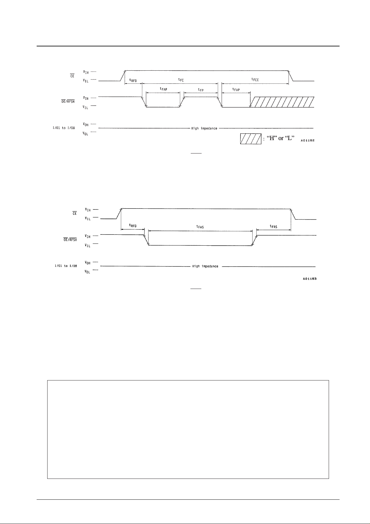
Timing Chart
Read Cycle
Write Cycle

Read-Write Cycle
CE-Only Refresh Cycle
LC33832P, S, M, PL, SL, ML-70/80/10
No. 4430-8/9
No. 4430-9/9
LC33832P, S, M, PL, SL, ML-70/80/10
Auto-Refresh Cycle
Note: A0 to A14, WE: “H” or “L”
Self-Refresh Cycle
Note: A0 to A14, WE: “H” or “L”
This catalog provides information as of February, 1997. Specifications and information herein are subject to
change without notice.
■ No products described or contained herein are intended for use in surgical implants, life-support systems, aerospace
equipment, nuclear power control systems, vehicles, disaster/crime-prevention equipment and the like, the failure of
which may directly or indirectly cause injury, death or property loss.
■ Anyone purchasing any products described or contained herein for an above-mentioned use shall:
➀ Accept full responsibility and indemnify and defend SANYO ELECTRIC CO., LTD., its affiliates, subsidiaries and
distributors and all their officers and employees, jointly and severally, against any and all claims and litigation and all
damages, cost and expenses associated with such use:
➁ Not impose any responsibility for any fault or negligence which may be cited in any such claim or litigation on
SANYO ELECTRIC CO., LTD., its affiliates, subsidiaries and distributors or any of their officers and employees
jointly or severally.
■ Information (including circuit diagrams and circuit parameters) herein is for example only; it is not guaranteed for
volume production. SANYO believes information herein is accurate and reliable, but no guarantees are made or implied
regarding its use or any infringements of intellectual property rights or other rights of third parties.
 Loading...