

Page 1
Any and all SANYO products described or contained herein do not have specifications that can handle
applications that require extremely high levels of reliability, such as life-support systems, aircraft’s
control systems, or other applications whose failure can be reasonably expected to result in serious
physical and/or material damage. Consult with your SANYO representative nearest you before using
any SANYO products described or contained herein in such applications.
SANYO assumes no responsibility for equipment failures that result from using products at values that
exceed, even momentarily, rated values (such as maximum ratings, operating condition ranges,or other
parameters) listed in products specifications of any and all SANYO products described or contained
herein.
Monolithic Digital IC
3-Channel Clock Driver
Ordering number:ENN3029B
LB8902M
SANYO Electric Co.,Ltd. Semiconductor Company
TOKYO OFFICE Tokyo Bldg., 1-10, 1 Chome, Ueno, Taito-ku, TOKYO, 110-8534 JAPAN
Overview
• The LB8902M is designed to drive a capacitive load at a
high speed.
• Suited for horizontal clock drive of CCD image sensor.
Functions and Features
• 3-channel inverter buffer amplifier.
• Fast propagation time (10ns typ. for 100pF load).
• Low-voltage operation available (5V min).
• Low quiescent current (10µA max).
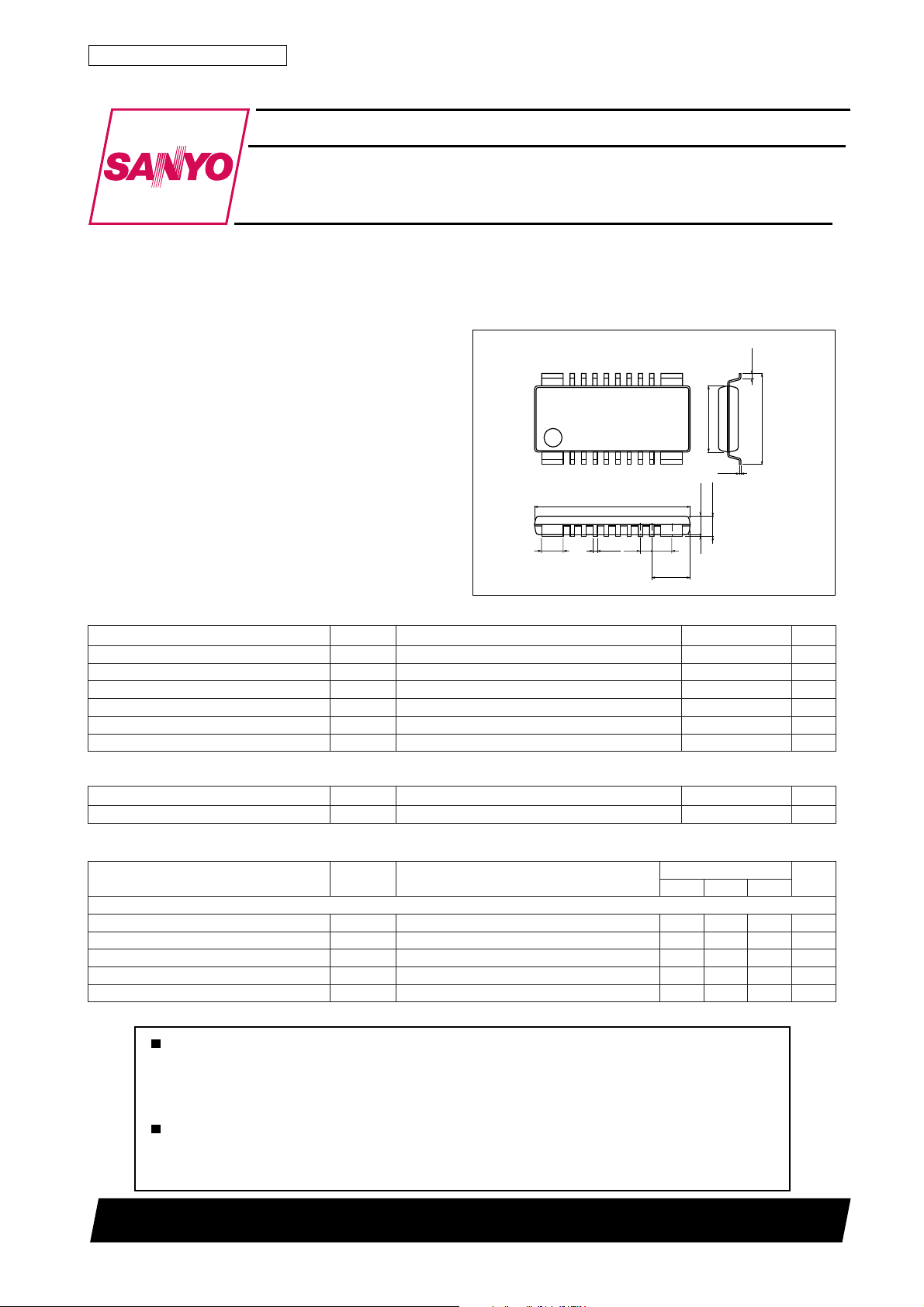
Package Dimensions
unit:mm
3097A-MFP16FS
[LB8902M]
16
1
9
5.4
8
0.15
0.63
7.6
12.4
1.35
0.35
1.0
Specifications
Absolute Maximum Ratings at Ta = 25˚C
retemaraPlobmySsnoitidnoCsgnitaRtinU
egatlovylppusmumixaMV
egatlovylppustupnIV
tnerructuptuomumixaMI
noitapissidrewopelbawollAxamdP 009Wm
erutarepmetgnitarepOrpoT 07+ot01–
erutarepmetegarotSgtsT 521+ot04–
Allowable Operating Ranges at Ta = 25˚C
retemaraPlobmySsnoitidnoCsgnitaRtinU
egatlovgnitarepO 11ot5V
Electrical Characteristics (DC Characteristics) at Ta = 25˚C, VCC1=VCC2=11V
retemaraPlobmySsnoitidnoC
]tnerruCegakaeL[
VssorcA
CC
DNGdna1kaeLI 01Aµ
VdnaNIssorcA
CC
DNGdnaNIssorcA3kaeLIVNIV6= 01Aµ
VdnaTUOssorcA
CC
DNGdnaTUOssorcA5kaeLIV
xam 0.21+ot3.0–V
CC
NI
TUO
2kaeLIVNIV0= 01Aµ
4kaeLIV
V0=01Aµ
TUO
V11=01Aµ
TUO
(1.5)
1.5
0.1
(2.7)
nimpytxam
1.7max
SANYO : MFP16FS
0.6+ot3.0–V
051Am
sgnitaR
˚C
˚C
tinU
22801TN (KT)/N2195YK/4050YT/N148TA, TS No.3029–1/4
Page 2
LB8902M
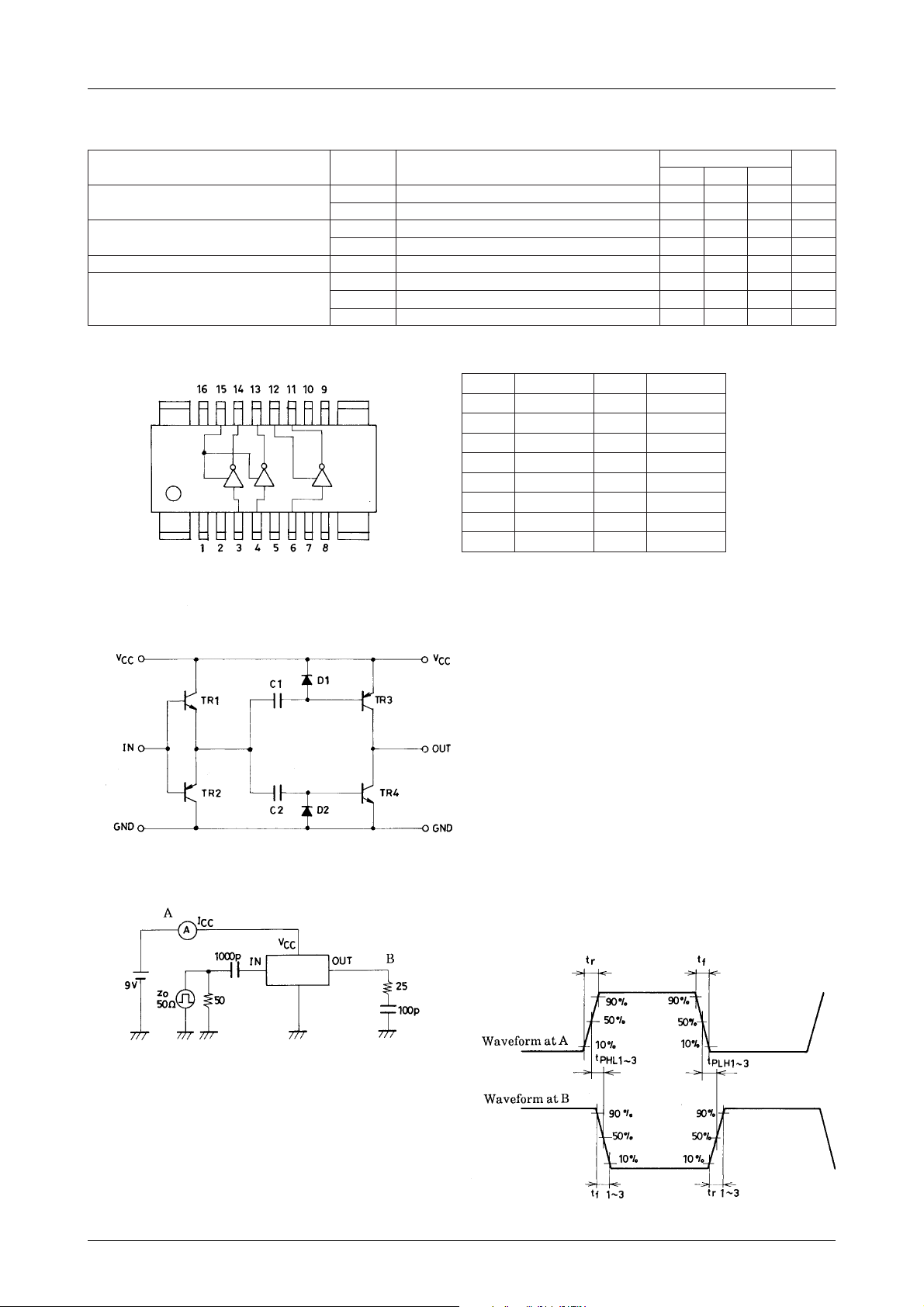
Switching Characteristics at Ta = 25˚C, VCC1=VCC2=9V, Vin=5Vp-p (f=14.3MHz), tr, tf≤6ns, load conditions :
RL=25Ω, CL=100pF
sgnitaR
V
CC
2
1
emitnoitagaporP
emittneisnarT
edutilpmatuptuOV
niardtnerruC
Pin Assignment
retemaraPlobmySsnoitidnoC
t
3-1.A.giFeeS0151sn
HLP
t
3-1.A.giFeeS851sn
LHP
tr3-1.A.giFeeS851sn
tf3-1.A.giFeeS851sn
P-PO
ICC1.A.giFeeS23Am
ICC2.A.giFeeS23Am
ICC3.A.giFeeS23Am
.A.giFeeS
1DNGemarF9DNGemarF
2DNG01.C.N
31NI113TUO
42NI21V
5DNG312TUO
63NI411TUO
7.C.N51V
8DNGemarF61DNGemarF
Note) Do not use the N.C. pin.
nimpytxam
VCC8.0–
.oNniPnoitcnuF.oNniPnoitcnuF
CC
CC
tinU
p-pV
Equivalent Circuit Block Diagram
Test Circuit
Unit (resistance : Ω, capacitance : F)
Fig. A Propagation Time, Transient Time
No.3029–2/4
Page 3

LB8902M
Proper Cares to be Taken in Designing a Printed Circuit Board
The LB8902M is designed to drive a load at a very high speed. When designing a printed circuit board, keep in mind the
following points.
1) Make the pattern of the power supply, GND lines as large as possible.
2) Place the bypass capacitor as close to the IC as possible (less than 1cm).
3) Make the wiring of the input signal line as short as possible to minimize the effect of stray capacitance.
4) Make the wiring of the output signal line also as short as possible, because the inductance of a long signal line may affect
the output waveforms adversely.
Take such necessary measures that a small resistance is inserted in series with a load.
Sample Application Circuit : Camera Block Diagram
No.3029–3/4
Page 4

LB8902M
Specifications of any and all SANYO products described or contained herein stipulate the performance,
characteristics, and functions of the described products in the independent state, and are not guarantees
of the performance, characteristics, and functions of the described products as mounted in the customer's
products or equipment. To verify symptoms and states that cannot be evaluated in an independent device,
the customer should always evaluate and test devices mounted in the customer's products or equipment.
SANYO Electric Co., Ltd. strives to supply high-quality high-reliability products. However, any and all
semiconductor products fail with some probability. It is possible that these probabilistic failures could
give rise to accidents or events that could endanger human lives, that could give rise to smoke or fire,
or that could cause damage to other property. When designing equipment, adopt safety measures so
that these kinds of accidents or events cannot occur. Such measures include but are not limited to protective
circuits and error prevention circuits for safe design, redundant design, and structural design.
In the event that any or all SANYO products(including technical data,services) described or
contained herein are controlled under any of applicable local export control laws and regulations,
such products must not be exported without obtaining the export license from the authorities
concerned in accordance with the above law.
No part of this publication may be reproduced or transmitted in any form or by any means, electronic or
mechanical, including photocopying and recording, or any information storage or retrieval system,
or otherwise, without the prior written permission of SANYO Electric Co. , Ltd.
Any and all information described or contained herein are subject to change without notice due to
product/technology improvement, etc. When designing equipment, refer to the "Delivery Specification"
for the SANYO product that you intend to use.
Information (including circuit diagrams and circuit parameters) herein is for example only ; it is not
guaranteed for volume production. SANYO believes information herein is accurate and reliable, but
no guarantees are made or implied regarding its use or any infringements of intellectual property rights
or other rights of third parties.
This catalog provides information as of February, 2001. Specifications and information herein are subject
to change without notice.
PS No.3029–4/4
 Loading...