

Page 1
Any and all SANYO products described or contained herein do not have specifications that can handle
applications that require extremely high levels of reliability, such as life-support systems, aircraft’s
control systems, or other applications whose failure can be reasonably expected to result in serious
physical and/or material damage. Consult with your SANYO representative nearest you before using
any SANYO products described or contained herein in such applications.
SANYO assumes no responsibility for equipment failures that result from using products at values that
exceed, even momentarily, rated values (such as maximum ratings, operating condition ranges,or other
parameters) listed in products specifications of any and all SANYO products described or contained
herein.
Monolithic Digital IC
CCD Clock Driver
Ordering number:ENN3030A
LB8901M
SANYO Electric Co.,Ltd. Semiconductor Company
TOKYO OFFICE Tokyo Bldg., 1-10, 1 Chome, Ueno, Taito-ku, TOKYO, 110-8534 JAPAN
Overview
The LB8901M is a monolithic IC designed to drive largecapacity clock gates of a CCD image sensor (LC9900 se-
ries) at a high speed.
Features
• Capable of driving large-capacity gates of a CCD, etc.
• On-chip eight-block driver, two of which are capable of
providing drive on the three-value level (LC9900 series).
No more than one chip is required to drive vertical gates.
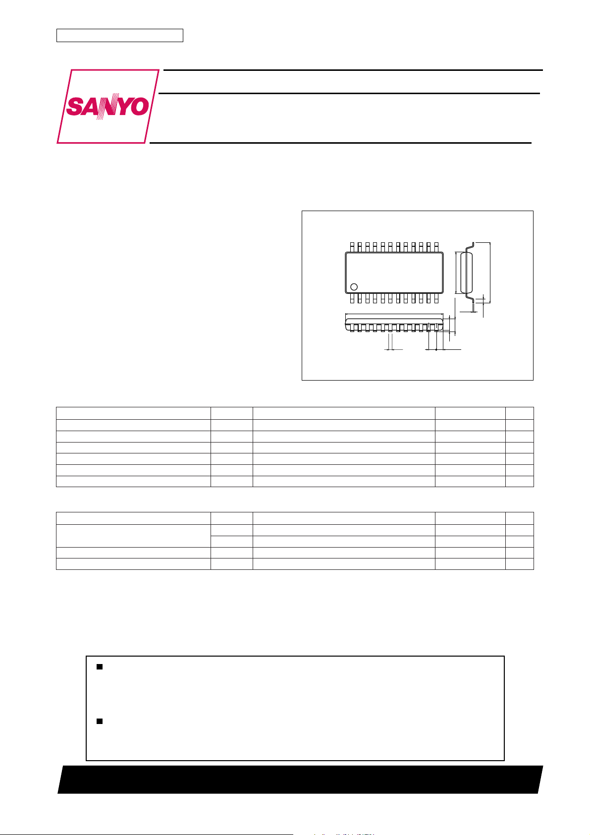
• Placed in a 24-pin miniflat package (MFP24S), facilitating miniaturization of equipment.
• Capable of being driven direct with TTL, CMOS, etc.
• A po wer sav e circuit can be connected to permit less power
dissipation.
Specifications
Absolute Maximum Ratings at Ta = 25˚C
retemaraPlobmySsnoitidnoCsgnitaRtinU
egatlovylppusmumixaMV
egatlovylppustupnIV
tnerructuptuomumixaMI
noitapissidrewopelbawollAxamdP 026Wm
erutarepmetgnitarepOrpoT 07+ot01–
erutarepmetegarotSgtsT 521+ot04–
xamVhcaE
CC
NI
TUO
Package Dimensions
unit:mm
3112A-MFP24S
[LB8901M]
24
112
nip0.81+ot3.0–V
CC
niptupnihcaE 0.6+ot3.0–V
niptuptuohcaE 052Am
12.5
0.35
13
5.4
1.7max
1.5
0.1
1.0
(0.75)
7.6
0.15
0.63
SANYO : MFP24S
˚C
˚C
Allowable Operating Ranges at Ta = 25˚C
retemaraPlobmySsnoitidnoCsgnitaRtinU
V
egatlovylppuS
egatlovlevel-hgihtupnIV
egatlovlevel-woltupnIV
CC
∆VCC2-1 VCCV–1CC2 ecnereffidegatlov
HI
LI
VhcaE
nip81ot5V
CC
niptupnihcaE 0.6ot5.2V
niptupnihcaE 3.0+ot3.0–V
22801TN (KT)/62194HK/N148TA, TS No.3030–1/5
0.6ot0V
Page 2
LB8901M
Electrical Characteristics at Ta = 25˚C, VCC1=9.0V, VCC2 to 5=13.0V
retemaraPlobmySsnoitidnoC
IHI1VIV,1
tnerruclevel-hgihtupnI
tnerruclevel-woltupnI
tnerrucylppuS
egatlovtuptuO
IHI2VFIV,
IHI3VIV,2
IHI4V
ILI1VIV,4ot1
ILI2VFIV,
I
1V;tupnihcaE
HCC
I
2V;tupnihcaE
HCC
I
3V;tupnihcaE
HCC
I
4V;tupnihcaE
HCC
I
5V;tupnihcaE
HCC
I
1V;tupnihcaE
LCC
I
2V;tupnihcaE
LCC
I
3V;tupnihcaE
LCC
I
4V;tupnihcaE
LCC
I
5V;tupnihcaE
LCC
VHO1VIV,V0=1
VHO2VIV,V0=1
VHO3VIV,V0=3
VHO4VIV,V5=3
VHO5VIV,2
VHO6VSV,3
VHO7VSV,1
V
LO
I
SI
I
S
S
SI
NI
NI
NI
NI
NI
V0=003Aµ
NI
V0=001Aµ
NI
V0=001Aµ
NI
V0=001Aµ
NI
V0=001Aµ
NI
V5=V
FI
V0=V
FI
V5=V
SI
V0=V
SI
V0=4V
I
V0=4V
S
V0=2V
S
VtupnihcaE
V5=0.1V
NI
V,2,1skcolbfostupni3
NI
V,2,1skcolbfostupni
NI
V,4,3skcolbfostupni4
NI
V,8ot5skcolbfostupni4ot1
V,2,1skcolbfostupni
V0.5=5.01Am
V0.5=0.48Am
V0.5=0.48Am
V0.5=0.48Am
V0.5=0.48Am
NI
sgnitaR
nimpytxam
V0.5=0.12Am
V0.5=0.12Am
V0.5=0.12Am
V0.5=0.12Am
NI
V,8ot1skcolbfostupni4ot1
V0=03–Aµ
NI
V0=001–02–Aµ
0.2–2V
CC
0.1–1V
CC
0.2–2V
CC
0.1–1V
CC
0.2–3V
CC
0.2–4V
CC
0.2–5V
CC
tinU
Switching Characteristics at Ta = 25˚C, VCC1=9.0V, VCC2 to 5=13.0V, VIN=5.0V, tr, tf≤10ns
retemaraPlobmySsnoitidnoC
t
1V;stuptuo3,1ø
level-wolemitnoitagaporP → level-hgih
level-hgihemitnoitagaporP → level-wol
emitesirtneisnarT
emitllaftneisnarT
HLP
t
2V;stuptuo3,1ø
HLP
t
3stuptuo4ot1Sø,4,2ø03sn
HLP
t
1V;stuptuo3,1ø
LHP
t
2V;stuptuo3,1ø
LHP
t
3stuptuo4ot1Sø,4,2ø03sn
LHP
tr1V;stuptuo3,1ø
tr2V;stuptuo3,1ø
tr3stuptuo4ot1Sø,4,2ø03sn
tf1V;stuptuo3,1ø
tf2V;stuptuo3,1ø
tf3stuptuo4ot1Sø,4,2ø03sn
Note : Load conditions
· Positive three-value driver (ø1, 3) ..................................... RS=16Ω, CL=1200pF
· Positive two-value driver (ø2, 4, øS1 to 4) ........................ RS=20Ω, CL=1300pF
FIV,SI
I
FIV,SI
I
FIV,SI
I
FIV,SI
I
dexifV0.5=03sn
V,1
I
V,1
I
V,1
I
V,1
I
dexifV0.5=32sµ
dexifV0.5=03sn
dexifV0.5=31sµ
dexifV0.5=03sn
dexifV0.5=36sµ
dexifV0.5=03sn
dexifV0.5=3003sn
nimpytxam
sgnitaR
tinU
No.3030–2/5
Page 3

LB8901M
Equivalent Circuit Block Diagram
Pin Function
.oNniPemaNniPnoitpircseDniP
1
2
3
4
5
6
7
8
9
01
11
21
31
41DNGnipdnuorG
51
61
71
81
91
02
12
22
32
42
VCC2
VCC1
1ø
2ø
3ø
4ø
VCC3
VCC4
VCC5
VS3
VS2
VS1
VS4
VI4
VI2
VI3
VI1
V
SI
V
3,1øtaesluptfihsemarfrofylppusrewoP
3,1øtaeslupeulav-eerhtrofylppusrewoP
DCCfo1ørof,tuptuoevirdeulav-eerhtevitisoP
DCCfo3ørof,tuptuoevirdeulav-eerhtevitisoP
DCCfo2ørof,tuptuoevirdeulav-owtevitisoP
DCCfo4ørof,tuptuoevirdeulav-owtevitisoP
4Sø
1Sø
2Sø
3Sø
4,2ørofylppusrewoP
4S,3SørofylppusrewoP
2S,1SørofylppusrewoP
revird3SøroftupnikcolC
revird2SøroftupnikcolC
revird1SøroftupnikcolC
revird4SøroftupnikcolC
revird4øroftupnikcolC
revird2øroftupnikcolC
revird3øroftupnikcolC
revird1øroftupnikcolC
revird3øroftupnieslupeulav-eerhT
FI
revird1øroftupnieslupeulav-eerhT
DCCfo4Sørof,tuptuoevirdeulav-owtevitisoP
DCCfo1Sørof,tuptuoevirdeulav-owtevitisoP
DCCfo2Sørof,tuptuoevirdeulav-owtevitisoP
DCCfo3Sørof,tuptuoevirdeulav-owtevitisoP
Sample Application Circuit : Camera Block Diagram
Proper Cares to be Taken in Designing a Printed Circuit Board
The LB8901M draws a large instantaneous current when it driv es a load. The LB8901M is also designed to drive a load at
a very high speed. When designing a printed circuit board, keep in mind the following points to prevent the output waveforms from being adversely affected.
1) Make the pattern of the power supply, GND lines as large as possible.
2) Place the bypass capacitor as close to the IC as possible (less than 1cm).
3) Make the wiring of the input signal line as short as possible to minimize the effect of stray capacitance.
4) Make the wiring of the output signal line also as short as possible, because the inductance of a long signal line may affect
the output waveforms adversely.
Take such necessary measures that a small resistance is inserted in series with a load.
5) When using a power save circuit, place it also as close to the IC as possible.
No.3030–3/5
Page 4

Switching Waveforms
tuptuO
tupnI
HGIHV
LO
WOLVHO7ot5
1) Blocks 1, 2
LB8901M
2) Blocks 3 to 8
Truth Table
VIV,1I3
tupnI
Truth Table
VFIV,
SI
HGIHWOL
HGIHVLOVHO4,2
WOLVHO3,1tibihnI
stupni
No.3030–4/5
Page 5

LB8901M
Specifications of any and all SANYO products described or contained herein stipulate the performance,
characteristics, and functions of the described products in the independent state, and are not guarantees
of the performance, characteristics, and functions of the described products as mounted in the customer's
products or equipment. To verify symptoms and states that cannot be evaluated in an independent device,
the customer should always evaluate and test devices mounted in the customer's products or equipment.
SANYO Electric Co., Ltd. strives to supply high-quality high-reliability products. However, any and all
semiconductor products fail with some probability. It is possible that these probabilistic failures could
give rise to accidents or events that could endanger human lives, that could give rise to smoke or fire,
or that could cause damage to other property. When designing equipment, adopt safety measures so
that these kinds of accidents or events cannot occur. Such measures include but are not limited to protective
circuits and error prevention circuits for safe design, redundant design, and structural design.
In the event that any or all SANYO products(including technical data,services) described or
contained herein are controlled under any of applicable local export control laws and regulations,
such products must not be exported without obtaining the export license from the authorities
concerned in accordance with the above law.
No part of this publication may be reproduced or transmitted in any form or by any means, electronic or
mechanical, including photocopying and recording, or any information storage or retrieval system,
or otherwise, without the prior written permission of SANYO Electric Co. , Ltd.
Any and all information described or contained herein are subject to change without notice due to
product/technology improvement, etc. When designing equipment, refer to the "Delivery Specification"
for the SANYO product that you intend to use.
Information (including circuit diagrams and circuit parameters) herein is for example only ; it is not
guaranteed for volume production. SANYO believes information herein is accurate and reliable, but
no guarantees are made or implied regarding its use or any infringements of intellectual property rights
or other rights of third parties.
This catalog provides information as of February, 2001. Specifications and information herein are subject
to change without notice.
PS No.3030–5/5
 Loading...