

Page 1
Ordering number : EN4946A
73196RM/51795TH (OT) No. 4946-1/12
Applications
The LB8108M is an actuator driver for use in portable CD
players that operate at a power supply voltage of 2.4 (two
nicad batteries) or 3.0 V (two dry-cell batteries).
Functions and Features
• Includes four H bridge driver channels to drive the four
CD player actuators (focus coil, tracking coil, spindle
motor and sled motor).
(output dynamic range: maximum of about 2 V)
• Includes a 3.9 V (typical) step-up circuit to supply the
DSP, ASP and microprocessor used in the CD player.
Also includes another voltage step-up circuit whose
voltage can be set with external resistors.
(However, note that the transistors, inductors, capacitors
and diodes required for drive operation are all external
components.)
• Built-in oscillator circuit for these converters
(external resistor and capacitor required)
• Detects the maximum value of the four driver outputs
and supplies a voltage slightly higher than that voltage
to the H bridge block in each of the four channels using
PWM voltage converter. This allows a drive scheme
with extremely low loss to be implemented.
(However, note that the pnp transistor, inductor,
capacitor, and diodes for the PWM circuit are all
external components.)
• Built-in laser diode drive and APC circuits
(IOmax ≈ 100 mA. This function can be turned off by a
control voltage input. It is composed of step-up
converter and series regulator.
However, note that the transistors, inductors, capacitors
and diodes required for drive operation are all external
components.)
• The sled motor drive circuit operates in 2 modes, that
are normal V-type drive mode and step drive mode
which is highly effective in reducing power dissipation.
• A step-down converter that convert external input
voltage that exceed 5 V into 3.5 V VCCoperates when
an external voltage input is applied. This simplifies
power supply design and thermal design for applying
VCC.
(This circuit turns on at the same time an external
voltage is applied and generates a 3.5 V VCC, which is
utilize for nicad battery charging.)
• Built-in microprocessor reset circuit (external capacitor
required)
(This circuit detects the VCDpin voltage and operates a
reset voltage with an H-side of 2.2 V (typical) and an Lside of 2.1 V (typical).)
• Two built-in battery check comparator channels
• System start and stop under microprocessor control
• Actuator muting function included.
(all four channels at the same time)
• Built-in thermal shutdown circuit
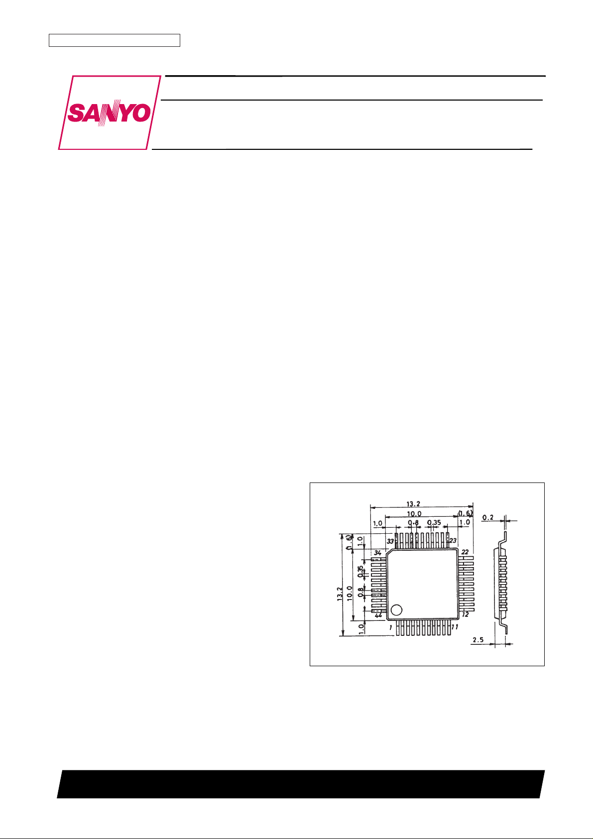
Package Dimension
unit: mm
3148-QFP44MA
SANYO: QIP44MA
[LB8108M]
LB8108M
SANYO Electric Co.,Ltd. Semiconductor Bussiness Headquarters
TOKYO OFFICE Tokyo Bldg., 1-10, 1 Chome, Ueno, Taito-ku, TOKYO, 110-8534 JAPAN
Actuator Driver for Portable CD Players
Monolithic Digital IC
Page 2
Specifications
Absolute Maximum Ratings at Ta = 25°C
Allowable Operating Ranges at Ta = 25°C
Electrical Characteristics at Ta = 25°C, VCC= 3 V
No. 4946-2/12
LB8108M
Parameter Symbol Conditions Ratings Unit
Maximum supply voltage V
CC
max 7 V
External input voltage V
EXT
max 9 V
H bridge output current I
OUT
max Taking 400 mA per channel as the maximum. 800 mA
Step-up circuit output current I
CD
max 150 mA
Allowable power dissipation Pd max Independent IC 900 mW
Operating temperature Topg –20 to +75 °C
Storage temperature Tstg –55 to +150 °C
Parameter Symbol Conditions Ratings Unit
Supply voltage V
CC
1.6 to 3.5 V
External input voltage V
EXT
5.0 to 8.0 V
Parameter Symbol Conditions min typ max Unit
[Power Supply Block]
Standby current drain I
CCO
S/S = high 100 µA
Quiescent current I
CC
S/S = low, with no drive input 16 25 mA
[Step-up Circuit (3.9 V)]
Step-up output voltage V
CD
3.7 3.9 4.1 V
NPN drive current I
D CD
3.0 mA
Load regulation R
LD CD
1000 mV/A
Line regulation R
LN CD
100 mV/V
Minimum off duty D
MIN CD
50 %
[Externally Set Step-Up Circuit]
NPN drive current I
D UP
3.0 mA
Input bias current I
B UP
200 nA
Minimum off duty D
MIN UP
50 %
[H Bridge Output Block, PWM Block]
Output saturation voltage V
H satIO
= 200 mA, TOP + BOTTOM 0.30 0.45 V
Maximum output voltage V
PWM
max 2.25 V
PNP drive current I
D PWM
V
OUT
/600 mA
Load regulation R
LD PWM
1000 mV/A
Line regulation R
LN PWM
100 mV/V
[Drive Control Block]
Input bias current I
B IN
2.0 µA
ASP reference input voltage range V
ASPR
1.2 VCD– 1.3 V
Transfer gain G
IN
For RL= 10 Ω 7.95 dB
Transfer gain difference (+/-) ∆G
IN
For RL= 10 Ω –1.0 0 +1.0 dB
Input dead zone voltage V
DZ
–30 0 +30 mV
[Sled Drive Circuit]
SLREF input voltage range V
SLREF
VCD– 0.5 V
Input bias current I
B SLED
200 nA
SLM on voltage V
SLM
2.0 V
[Oscillator Block]
Oscillator power output voltage V
OSCP
VCC– 0.15 V
Oscillator maximum frequency F
MAX
100 kHz
OSC pin input bias current I
B OSC
–2.0 µA
Continued on next page.
Page 3
Continued from preceding page.
Note: 1. V
HSENSE
and V
LSENSE
will never be inverted in any individual IC.
2. Items specified to be a design target value in the conditions column are not measured.
No. 4946-3/12
LB8108M
Parameter Symbol Conditions min typ max Unit
[Battery Check Block]
BI1 and BI2 input bias current I
B BI1, 2
200 nA
BO1 and BO2 output
V
BO1, 2
For IO= 500 µA 0.3 V
saturation voltage
[S/S Pin Function]
S/S start voltage V
SS ON
VCC– 1.0 V
S/S off voltage V
SS OFF
VCC– 0.5 V
[External Voltage Input Block]
Minimum operating input voltage V
I EXT
5.0 V
PNP drive current I
D EXT
3.0 mA
Step-down circuit output voltage V
O EXT
3.3 3.5 3.7 V
[Muting Block]
Muting on voltage V
MUTE
2.0 V
[APC Circuit Block]
Maximum output current I
O APC
100 mA
LDCTL pin input bias current I
B LDC
–5.0 µA
LDCTL off voltage V
LDOFF
0.4 V
MDin pin input bias current I
B MDIN
–1.0 µA
VLD step-up voltage V
LDOUT
Taking V
LDO
as the reference 0.3 V
NPN drive current I
D LDO
1.0 mA
[Reset Circuit Block]
Reset charge current I
CHG
–1.25 µA
Output saturation voltage V
RST
For IO= 100 µA 0.3 V
H side detection voltage V
HSENSE
For the VCDpin voltage
*1
2.1 2.2 2.3 V
L side detection voltage V
LSENSE
For the VCDpin voltage
*1
2.0 2.1 2.2 V
[TSD Block]
TSD operating temperature T
TSD
Design target value
*2
180 °C
TSD temperature hysteresis ∆T
TSD
Design target value
*2
20 °C
Page 4
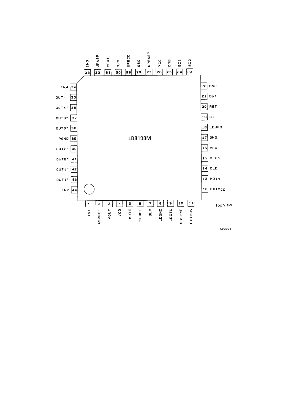
Pin Assignment
No. 4946-4/12
LB8108M
Page 5

Pin Functions
No. 4946-5/12
LB8108M
Pin No. Symbol Equivalent circuit Function
1, 44
33, 34
2
43, 42
41, 40
38, 37
36, 35
3, 31
4
5
6
7
8
IN1, IN2
IN3, IN4
ASPREF
OUT1+, 1–
OUT2+, 2–
OUT3+, 3–
OUT4+, 4–
V
OUT
V
CD
MUTE
SLREF
SLM
LD GND
The actuator control signals corresponding to
IN1: focus, IN2: tracking, IN3: spindle, IN4:
sled. Input from the ASP (DSP).
Focus coil actuator drive output
Tracking coil actuator drive output
Spindle motor drive output
Sled motor drive output
(Each channel includes built-in spark killer
diodes.)
Power supply for the four H bridge driver
channels. An external PWM step-up circuit
can be used to generate a voltage slightly
higher than the maximum voltage output by
any of the four output channels.
Input for the 3.9 V step-up circuit. The drive
control system operates on this voltage. This
voltage can also be supplied to other ICs in
the system, such as the DSP and the
microprocessor.
Input for muting of the four actuator channels
at the same time.
High: mute applied.
Threshold input used when operating the
sled motor in step drive mode.
Input that selects sled motor step drive
mode.
High: V-type selected
Low: Step mode
Dedicated ground connection for the internal
reference voltage for laser diode APC
control.
Connect to a ground near the laser diode.
Continued on next page.
Page 6

Continued from preceding page.
No. 4946-6/12
LB8108M
Pin No. Symbol Equivalent circuit Function
9
10
28
11
12
13
14
LDCTL
OSCPWR
OSC
EXTDRV
EXTV
CC
MD in
C
LD
Laser diode APC (auto power control) control
signal input. When this voltage falls under
about 0.4 V the APC output is turned off.
RC power supply for invalid current
prevention for the OSC oscillator circuit.
Input for the free-running oscillator circuit
used for PWM step-down and step-up
circuits. The oscillator frequency is
determined by an external RC circuit.
Base drive output for external step-down pnp
transistor used when external power is
applied.
External power supply input. This voltage is
converted into 3.5 V with a PWM step-down
circuit and supplied to V
CC
.
Input for the output from the laser diode APC
monitor diode.
Terminal for the capacitor that eliminates
high frequency from laser drive signal. This
capacitor is also useful for soft starting in the
LD output.
Continued on next page.
Page 7

Continued from preceding page.
No. 4946-7/12
LB8108M
Pin No. Symbol Equivalent circuit Function
15
16
17
18
25
27
29
19
20
21, 22
24, 23
V
LDO
V
LD
GND
LDUPB
DNB
UPBASP
UPBCD
CT
RST
BO1, BO2
BI1, BI2
Output that directly drives the laser diode.
I
O
max is about 100 mA.
Input in the laser APC circuit for the external
step-up circuit used to assure V
LDO
(i.e., to
assure V
CE
for the internal output transistor)
when V
CC
falls. VLDis controlled to 0.3 V
(typical) more than V
LDO
.
LB8108M small signal system ground (ground
for circuits without the output transistor)
Base drive circuit for external step-up npn
transistor in the laser APC circuit for the
external step-up circuit used to assure V
LDO
when VCCfalls.
Base drive output for the step-down PWM
pnp transistor that generates the power
supplied to the actuator H bridge drivers.
Base drive output for the external npn
transistor for the step-up circuit whose stepup voltage is set externally.
Base drive output for the 3.9 V step-up
external npn transistor.
Terminal for the reset circuit capacitor
(The reset time will be about 50 ms for a
0.1 µF capacitor.)
Reset circuit open collector output
Battery check comparator open collector
output
Battery check comparator input. This voltage
is compared to 1.2 V internally.
Continued on next page.
Page 8

Continued from preceding page.
No. 4946-8/12
LB8108M
Pin No. Symbol Equivalent circuit Function
26
30
32
39
V
CC
S/S
UPASP
PGND
Power supply connection
LB8108M start input (starts on a low level
input). No power on lock function is included.
Voltage feedback input for the externally set
step-up circuit. The step-up voltage is determined by comparing this voltage to 1.2 V.
Ground for the four H bridge driver channel
output transistors. This ground is not
connected to the small signal system ground
internally.
Page 9

Block Diagram
No. 4946-9/12
LB8108M
Page 10

Operating Description
Reset Function
The LB8108M includes a built-in circuit that outputs a reset signal to the control microprocessor. This circuit operates
when VCCis applied. (It does not depend on the S/S circuit.)
The reset time is determined by the capacitor connected to the CT pin, and will be about 50 ms for a 0.1 µF capacitor.
The level detection circuit detects the VCDvoltage as shown in the figure.
That is, the reset state is cleared by RST going from low to high after the passage of the time determined by CT starting
at the point the VCDvoltage exceeds 2.2 V (typical) after VCCis applied. At this time RST will remain cleared even if
S/S is turned on and VCDrises to 3.9 V (typical). Then, if S/S is turned off and the VCDvoltage returns to the voltage
determined by VCCand the Schottky diode voltage drop, and additionally, the VCDvoltage falls under 2.1 V (typical)
due to a drop in the battery voltage, reset is applied (turned on) again.
(In other words, there is hysteresis in the detection level.)
(Note that since the RST output has a limited drive current, it should be used with a pull-up resistor of about 100 kΩ.)
APC Function
In systems that used earlier drivers, the laser diode APC (auto power control) circuit that adopted an ASP (analog signal
processor) were generally used. However, this ASP was originally driven by the power supply stepped up from VCCby
the driver IC and the laser diode was then driven by a series type regulator supplied by that voltage. This had the
problem that the power dissipation was large.
This power dissipation takes a large part of the total power dissipation in the whole system, especially in portable
equipment. To reduce this power dissipation, the LB8108M takes the power for the laser diode directly from VCC.
(In practice, this circuit consists of an up converter and a series regulator. When the VCCvoltage is high enough, the
circuit operates as a series type circuit, but since these circuits are expected to be used in portable applications, that will
be relatively rare.)
Laser Diode Drive Technique in General Overview of the LB8108M Laser Diode Drive System
No. 4946-10/12
LB8108M
Page 11

No. 4946-11/12
LB8108M
First, when VCCis adequately high (about 2.5 V or over) the laser diode is driven by the system consisting of VCC, an
inductor and a Schottky diode without driving LDUPB. Then, when VCCfalls and VLD– V
LDO
become under about 0.3
V, LDUPB is driven, VLDis stepped up, and the circuit is controlled so that VLD– V
LDO
is held at 0.3 V (typical).
The following describes the laser diode intensity adjustment function supported by the LB8108M.
First, set up the pickup so that the monitor diode output is about 0.2 V in the normal usage range.
When LDCTL is in the range 0.0 to 0.5 V the LD drive function will be in the cutoff state and the laser diode will not be
driven. As the LDCTL voltage rises, the LD drive reference voltage shown in the figure varies between 0.1 and 0.3 V.
Then, the V
LDO
pin voltage is controlled so that the monitor diode output and that reference voltage become identical.
However, since the output current peak is 100 mA (typical), the output voltage will not increase when an output current
in excess of that value is required.
(Since the intensity adjustment will go to its maximum setting when the LDCTL pin is open, an appropriate voltage must
be applied to the LDCTL pin.)
Sled Control
The figure below shows the operation of the LB8108M’s sled actuator step control.
When the SLM pin is set high, the LB8108M operates in the normal V-type control mode. However, the LB8108M can
be set to operate in a sled drive mode that is highly efficient at
reducing power dissipation by setting the SLM pin low.
The step drive start level is input from the SLREF pin. (Only a
voltage higher than V
ASPREF
will be accepted.)
The circuit operates once in step drive mode following the locus
of line ➀in the figure. Then, on returning, it operates in V-type
control following the locus of line ➁.
Next, the circuit can be operated in step mode by putting the
input (VIN4) into the reverse region.
(If the input does not enter the reverse region, the circuit will
continue to operate in V-type mode.)
Page 12

PS No. 4946-12/12
LB8108M
This catalog provide information as of July, 1996. Specifications and information herein are subject to change
without notice.
■ No products described or contained herein are intended for use in surgical implants, life-support systems, aerospace
equipment, nuclear power control systems, vehicles, disaster/crime-prevention equipment and the like, the failure of
which may directly or indirectly cause injury, death or property loss.
■ Anyone purchasing any products described or contained herein for an above-mentioned use shall:
➀ Accept full responsibility and indemnify and defend SANYO ELECTRIC CO., LTD., its affiliates, subsidiaries and
distributors and all their officers and employees, jointly and severally, against any and all claims and litigation and all
damages, cost and expenses associated with such use:
➁ Not impose any responsibility for any fault or negligence which may be cited in any such claim or litigation on
SANYO ELECTRIC CO., LTD., its affiliates, subsidiaries and distributors or any of their officers and employees
jointly or severally.
■ Information (including circuit diagrams and circuit parameters) herein is for example only; it is not guaranteed for
volume production. SANYO believes information herein is accurate and reliable, but no guarantees are made or implied
regarding its use or any infringements of intellectual property rights or other rights of third parties.
 Loading...