

Page 1
Ordering number :EN5452A
41399TH (OT) / 73097HA (OT) No. 5452-1/9
Functions
• The LB1955 is a 3-phase brushless motor driver IC that
is optimal for applications such as driving the drum
motor in VCRs.
Features
• Current linear drive
• FG and PG free
• Single-voltage power supply
• Built-in AGC circuit
• Built-in thermal shutdown circuit
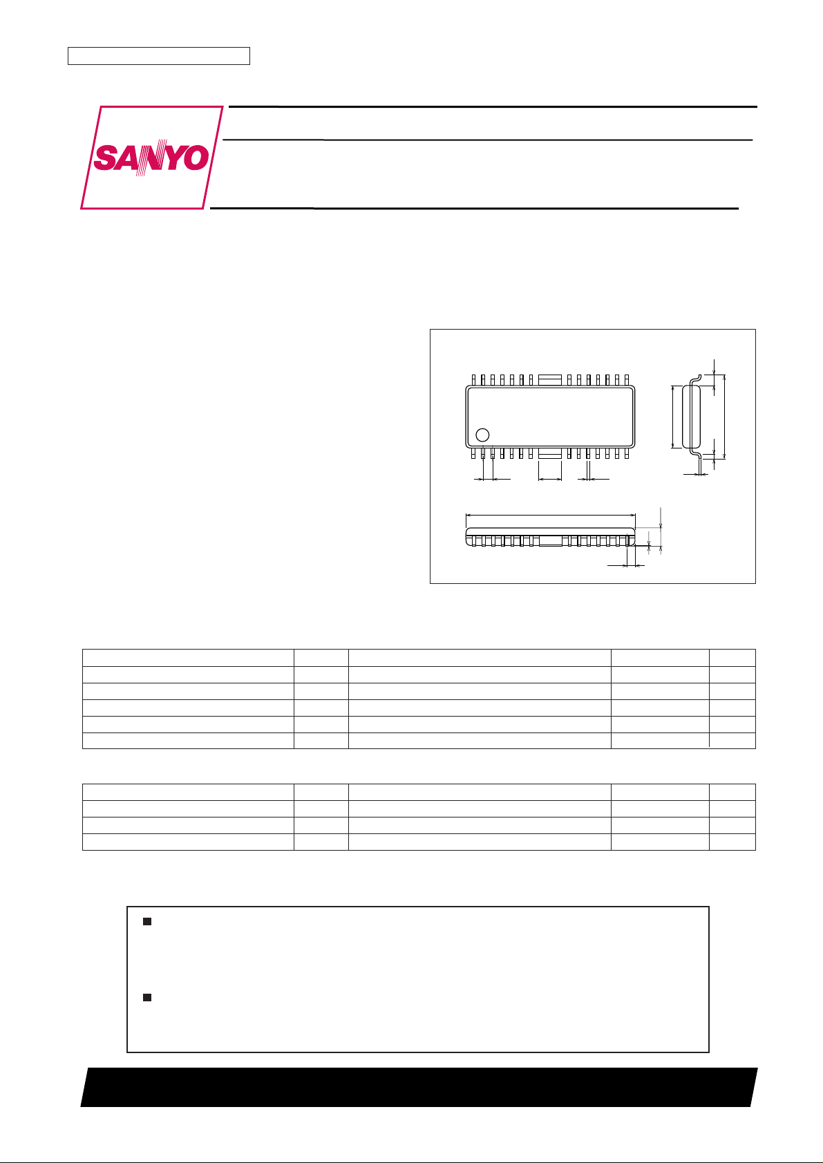
Package Dimensions
unit: mm
3222-HSOP28
0.1
1.8max
7.6
1.0
114
0.3
0.8
1528
2.7
15.2
0.8
5.6
0.5
0.2
SANYO: HSOP28
[LB1955]
SANYO Electric Co.,Ltd. Semiconductor Company
TOKYO OFFICE Tokyo Bldg., 1-10, 1 Chome, Ueno, Taito-ku, TOKYO, 110-8534 JAPAN
Monolithic Digital IC
LB1955
Three-Phase Brushless Motor Driver
Any and all SANYO products described or contained herein do not have specifications that can handle
applications that require extremely high levels of reliability, such as life-support systems, aircraft’s
control systems, or other applications whose failure can be reasonably expected to result in serious
physical and/or material damage. Consult with your SANYO representative nearest you before using
any SANYO products described or contained herein in such applications.
SANYO assumes no responsibility for equipment failures that result from using products at values that
exceed, even momentarily, rated values (such as maximum ratings, operating condition ranges, or other
parameters) listed in products specifications of any and all SANYO products described or contained
herein.
Parameter Symbol Conditions Ratings Unit
Maximum supply voltage V
CC
max 14.5 V
Maximum output current I
OUT
1.0 A
Allowable power dissipation Pdmax Independent device 0.60 W
Operating temperature Topr –20 to +75 °C
Storage temperature Tstg –55 to +150 °C
Specifications
Absolute Maximum Ratings at Ta = 25°C
Parameter Symbol Conditions Ratings Unit
Supply voltage V
CC
10.2 to 13.8 V
Hall input amplitude Vhall At the input 70 to 500 mVp-p
VC input voltage V
C
0 to 5 V
Allowable Operating Ranges at Ta = 25°C
Page 2
No. 5452-2/9
LB1955
Electrical Characteristics at Ta = 25°C, VCC= 12 V
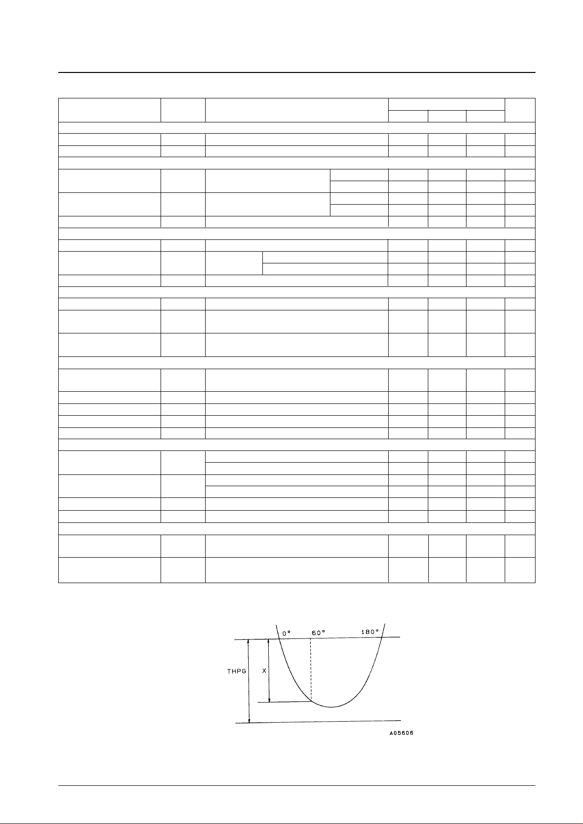
Note: * is provided for when X is the peak value at the 60° position of the lower side of the UIN1 Hall amplifier input: THPG = 1.17X.
However, note that the THPG level may be reduced if the value of the capacitor (SH) used for the sample-and-hold circuit is too small since
a discharge current of a few nA will result.
Parameter Symbol Conditions
Ratings
Unit
min typ max
[Power Supply]
Current drain I
CC
VC= 0 V, LCTR = 6 V 7.0 10.0 13.0 mA
IC internal power supply V
REF
4.75 5.0 5.25 V
[Output]
Output saturation voltage V
O(sat)
1
I
O
= 400 mA Sink side 0.4 V
V
C
= 5 V, Rf= 0 Ω Source side 1.5 V
Output saturation voltage 2 V
O(sat)
2
I
O
= 800 mA Sink side 0.7 V
V
C
= 5 V, Rf= 0 Ω Source side 2.0 V
3-phase output current ripple Ior I
O
= 100 mA, Rf = 0.47 Ω –5 +5 %
[Hall Amplifier]
Input offset voltage VHoff –20 +20 mV
Input bias current IHb
V
AGC
= 1.4 V
U
IN
10 µA
V
IN
, W
IN
5 µA
Common-mode input voltage range
V
HCM
2.2 5.0 V
[Control]
VC pin input bias current I
VCb
VC= 0 V –10 –1.3 µA
Control start voltage V
THVC
Rf= 0.47 Ω, IO≥ 10 mA
2.25 2.5 2.75 V
With the Hall input logic fixed
Open-loop control gain G
MVC
Rf= 0.47 Ω, ∆IO= 200 mA
0.72 0.9 1.08 A/V
With the Hall input logic fixed and VG shorted to RF
[PG]
PG Hall amplifier
V
PGoff
Design target –10 +10 mV
input offset voltage
Peak hold charge current I
SHCHG
(U, V, W) = (L, L, H) 30 µA
PG comparator threshold THPG SH = 1000pF, Design target* 113 117 121 %
PG output high-level voltage V
PGH
4.5 5.2 V
PG leakage current I
LEAKPG
–10 0 +10 µA
[FG]
Back emf Schmitt input
V
SCHG
In the back emf Schmitt input increasing direction, Design target 100 mV
hysteresis width
In the back emf Schmitt input decreasing direction, Design target 0 mV
Ringing canceller Schmitt
V
SCHR
In the Schmitt input increasing direction, Design target 180 mV
input hysteresis width
In the Schmitt input decreasing direction, Design target –20 0 +20 mV
FG output high-level voltage V
FGH
FGR = 0 V 4.5 5.2 V
FG leakage current I
LEAKFG
–10 0 +10 µA
[TSD]
Thermal shutdown
TTSD Design target 180 °C
operating temperature
Thermal shutdown
∆TSD Design target 15 °C
temperature hysteresis width
Page 3
No. 5452-3/9
LB1955
Allowable power dissipation, Pd max – W
Ambient temperature, Ta – °C
Pin Assignment
W
IN
2
W
IN
1
V
IN
2
V
IN
1
U
IN
2
U
IN
1
Pin Functions
Pin No. Pin Function
23, 24 U
IN
1, UIN2 U phase Hall element input
25, 26 V
IN
1, VIN2 V phase Hall element input
27, 28 W
IN
1, WIN2 W phase Hall element input
16 UOUT U phase output
15 VOUT V phase output
13 WOUT W phase output
11 LCTR Pin connected to the center points of the coils that are Y-connected to the U, V, and W outputs.
9 V
CC
Power supply
10 V
REF
Reference voltage output
8 GND GND
14 Rf Output current detection
1 VG Closed loop control gain switching
2 FC Speed control loop frequency characteristics correction
3 LIM Output current limit setting
4 VC Speed control
5 PG PG waveform output
6 FG FG waveform output (FGR shorted to GND)
7 FGR PG/FG synthesized output (FGR shorted to PG)
18 SH PG waveform sample-and-hold circuit capacitor connection
22 AGC Connection for the capacitor used by the AGC circuit, which holds the input gain at a fixed level.
12, 17, 19
NC No connection
20, 21
Page 4

No. 5452-4/9
LB1955
Source → sink
Hall input logic
U V W
1 W phase → V phase H H L
2 W phase → U phase H L L
3 V phase → U phase H L H
4 V phase → W phase L L H
5 U phase → W phase L H H
6 U phase → V phase L H L
Truth Table
Note: The Hall input "H" and "L" values are defined as follows: "H" means that for that phase the (+) input is higher than the (-) input, and "L" means that for
that phase the (+) input is lower than the (-) input. However, note that an input potential difference corresponding to the Hall to output gain is required.
Timing Charts
Note: The Hall inputs are defined as follows: U = UIN1 – UIN2, V = VIN1 – VIN2, and W = WIN1 – WIN2.
Inputs to the Hall input pins must be applied in the phase order shown in the timing chart.
Hall inputs
Synthesized
waveform
Page 5

No. 5452-5/9
LB1955
Recommended Special Magnetization Waveforms
Note: Note that the intersections between the special magnetization and general waveforms and the intersections between pairs of general waveforms must
be set up to be 30° apart.
Hall Input Order
Note: The Hall input order must be set up to be W → V → U.
B ≤ A < 7/6 × B
8/6 × D ≤ C ≤ 10/6 × D
Hall input
Page 6

VG and LIM Pin Usage
No. 5452-6/9
LB1955
LIM pin: Open
VG – Rf: Shorted
Gm = 0.423/Rf (A/V)
(Closed loop control gain)
Ilim = (V
REF
× 27/200 – 0.2) × 4.23/3/Rf
(Current limit)
VG pin: Open
Gm = 1/Rf (A/V)
(Closed loop control gain)
Ilim = (V
REF
×27/200 – 0.2) ×10/3/Rf
(Current limit)
LIM – V
REF
: Shorted
No current limit.
Note: This current limiting function is for protection against unusual and abnormal currents. If a current limit level below the rated current is set, this will,
inversely, result in heat generation within the IC.
When the LIM pin is open, VG is shorted to Rf, and Rf = 0.47 Ω, this will result in a current limit level of about 1.3 to 1.4 A. If this limit falls under the
rated value due to mode changes or changes in the value of the Rf resistor, set the current limit to an appropriate value by applying to the LIM pin a
voltage that is divided from the V
REF
to ground potential by resistors of a few kΩ. Alternatively, short the LIM pin to V
REF
to defeat the current limit
function.
Output
stage
PG and FG Pin Output Circuits FG (FGR shorted to ground)
PG (FGR shorted to PG)
Page 7

Block Diagram
No. 5452-7/9
LB1955
Hall input synthesis block
(linear matrix)
3-phase differential
distribution circuit
Power transistors
FG waveform
synthesis
PG waveform
synthesis
Internal power supply
UIN1
UIN2
VIN1
VIN2
WIN1
WIN2
Page 8

No. 5452-8/9
LB1955
Sample Application Circuit
LB1955
U
IN
1
U
IN
2
V
IN
2
V
IN
1
W
IN
1
W
IN
2
0 to 5 V
Page 9

PS No. 5452-9/9
LB1955
This catalog provides information as of April, 1999. Specifications and information herein are subject to
change without notice.
Specifications of any and all SANYO products described or contained herein stipulate the performance,
characteristics, and functions of the described products in the independent state, and are not guarantees
of the performance, characteristics, and functions of the described products as mounted in the customer’s
products or equipment. To verify symptoms and states that cannot be evaluated in an independent device,
the customer should always evaluate and test devices mounted in the customer’s products or equipment.
SANYO Electric Co., Ltd. strives to supply high-quality high-reliability products. However, any and all
semiconductor products fail with some probability. It is possible that these probabilistic failures could
give rise to accidents or events that could endanger human lives, that could give rise to smoke or fire,
or that could cause damage to other property. When designing equipment, adopt safety measures so
that these kinds of accidents or events cannot occur. Such measures include but are not limited to protective
circuits and error prevention circuits for safe design, redundant design, and structural design.
In the event that any or all SANYO products (including technical data, services) described or contained
herein are controlled under any of applicable local export control laws and regulations, such products must
not be exported without obtaining the export license from the authorities concerned in accordance with the
above law.
No part of this publication may be reproduced or transmitted in any form or by any means, electronic or
mechanical, including photocopying and recording, or any information storage or retrieval system,
or otherwise, without the prior written permission of SANYO Electric Co., Ltd.
Any and all information described or contained herein are subject to change without notice due to
product/technology improvement, etc. When designing equipment, refer to the “Delivery Specification”
for the SANYO product that you intend to use.
Information (including circuit diagrams and circuit parameters) herein is for example only; it is not
guaranteed for volume production. SANYO believes information herein is accurate and reliable, but
no guarantees are made or implied regarding its use or any infringements of intellectual property rights
or other rights of third parties.
 Loading...