Ordering number :EN5452
73097HA (OT) No. 5452-1/7
Functions
• The LB1955 is a 3-phase brushless motor driver IC that
is optimal for applications such as driving the drum
motor in VCRs.
Features
• Current linear drive
• FG and PG free
• Single-voltage power supply
• Built-in AGC circuit
• Built-in thermal shutdown circuit
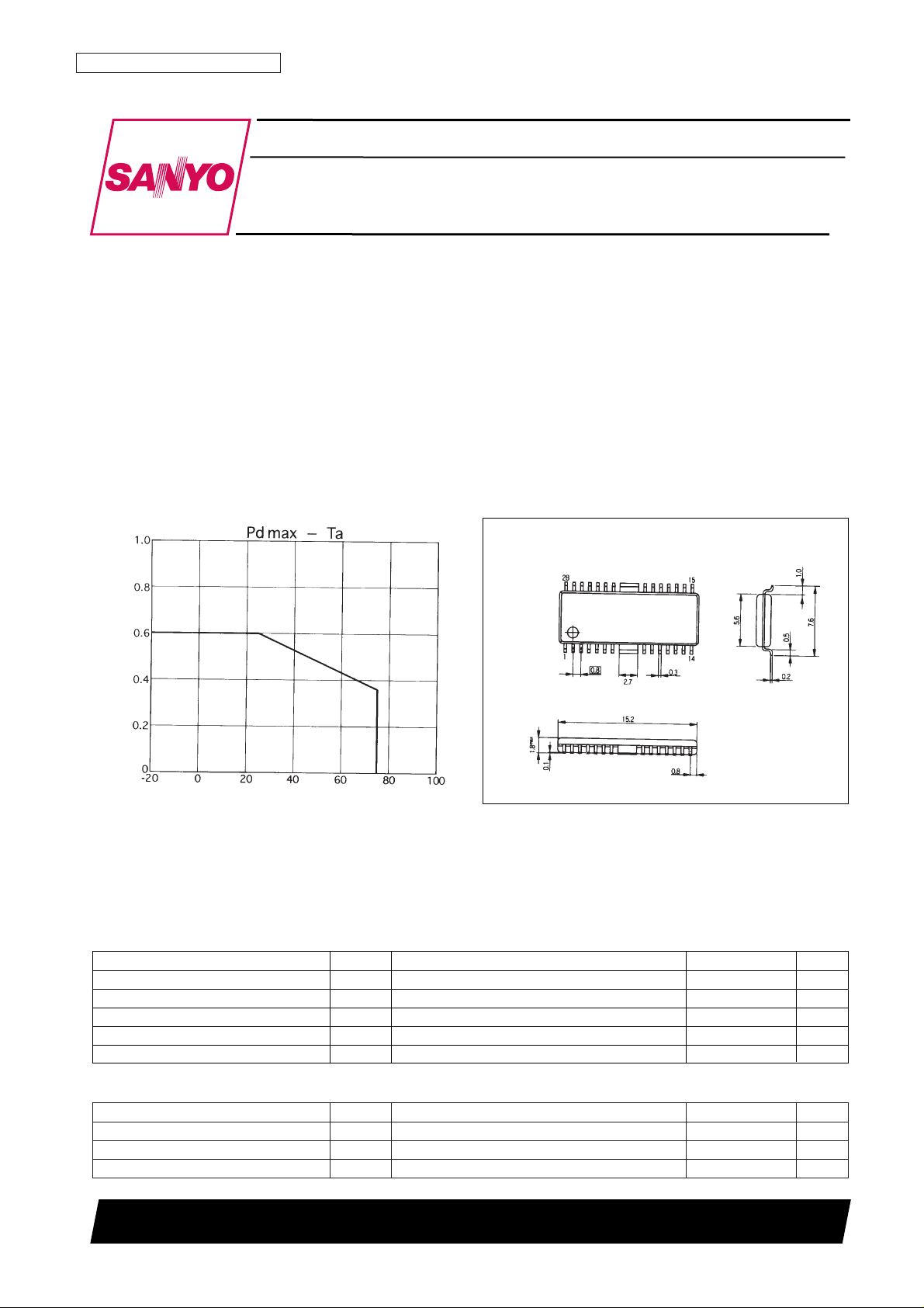
Package Dimensions
unit: mm
3222-HSOP28
SANYO: HSOP28
[LB1955]
SANYO Electric Co.,Ltd. Semiconductor Bussiness Headquarters
TOKYO OFFICE Tokyo Bldg., 1-10, 1 Chome, Ueno, Taito-ku, TOKYO, 110 JAPAN
Monolithic Digital IC
LB1955
Three-Phase Brushless Motor Driver
Parameter Symbol Conditions Ratings Unit
Maximum supply voltage V
CC
max 14.5 V
Maximum output current I
OUT
1.0 A
Allowable power dissipation Pdmax Independent device 0.60 W
Operating temperature Topr –20 to +75 °C
Storage temperature Tstg –55 to +150 °C
Specifications
Absolute Maximum Ratings at Ta = 25°C
Parameter Symbol Conditions Ratings Unit
Supply voltage V
CC
10.2 to 13.8 V
Hall input amplitude Vhall At the input 70 to 500 mVp-p
VC input voltage V
C
0 to 5 V
Allowable Operating Ranges at Ta = 25°C
Ambient temperature, Ta – °C
Allowable power dissipation, Pd max – W

No. 5452-2/7
LB1955
Electrical Characteristics at Ta = 25°C, VCC= 12 V
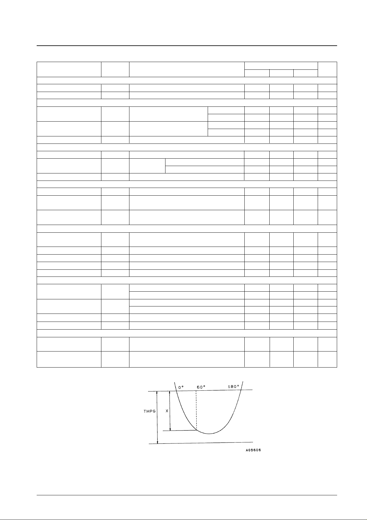
Note: * is provided for when X is the peak value at the 60° position of the lower side of the UIN1 Hall amplifier input: THPG = 1.17X.
Parameter Symbol Conditions
Ratings
Unit
min typ max
[Power Supply]
Current drain I
CC
VC= 0 V, LCTR = 6 V 7.0 10.0 13.0 mA
IC internal power supply V
REF
4.75 5.0 5.25 V
[Output]
Output saturation voltage V
O(sat)
1
I
O
= 400 mA Sink side 0.4 V
V
C
= 5 V, Rf= 0 Ω Source side 1.5 V
Output saturation voltage 2 V
O(sat)
2
I
O
= 800 mA Sink side 0.7 V
V
C
= 5 V, Rf= 0 Ω Source side 2.0 V
3-phase output current ripple Ior I
O
= 100 mA, Rf = 0.47 Ω –5 +5 %
[Hall Amplifier]
Input offset voltage VHoff –20 +20 mV
Input bias current IHb
V
AGC
= 1.4 V
U
IN
10 µA
V
IN
, W
IN
5 µA
Common-mode input voltage range
V
HCM
2.2 5.0 V
[Control]
VC pin input bias current I
VCb
VC= 0 V –10 –1.3 µA
Control start voltage V
THVC
Rf= 0.47 Ω, IO≥ 10 mA
2.25 2.5 2.75 V
With the Hall input logic fixed
Open-loop control gain G
MVC
Rf= 0.47 Ω, ∆IO= 200 mA
0.72 0.9 1.08 A/V
With the Hall input logic fixed and VG shorted to RF
[PG]
PG Hall amplifier
V
PGoff
Design target –10 +10 mV
input offset voltage
Peak hold charge current I
SHCHG
(U, V, W) = (L, L, H) 30 µA
PG comparator threshold THPG Design target* 117 %
PG output high-level voltage V
PGH
4.5 5.2 V
PG leakage current I
LEAKPG
–10 0 +10 µA
[FG]
Back emf Schmitt input
V
SCHG
In the back emf Schmitt input increasing direction, Design target 100 mV
hysteresis width
In the back emf Schmitt input decreasing direction, Design target 0 mV
Ringing canceller Schmitt
V
SCHR
In the Schmitt input increasing direction, Design target 180 mV
input hysteresis width
In the Schmitt input decreasing direction, Design target –20 0 +20 mV
FG output high-level voltage V
FGH
FGR = 0 V 4.5 5.2 V
FG leakage current I
LEAKFG
–10 0 +10 µA
[TSD]
Thermal shutdown
TTSD Design target 180 °C
operating temperature
Thermal shutdown
∆TSD Design target 15 °C
temperature hysteresis width

No. 5452-3/7
LB1955
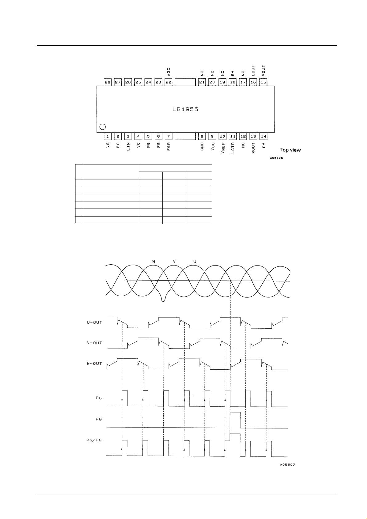
Pin Assignment
Source → sink
Hall input logic
U V W
1 W phase → V phase H H L
2 W phase → U phase H L L
3 V phase → U phase H L H
4 V phase → W phase L L H
5 U phase → W phase L H H
6 U phase → V phase L H L
Truth table
Note: The Hall input "H" and "L" values are defined as follows: "H" means that for that phase the (+) input is higher than the (-) input, and "L" means that for
that phase the (+) input is lower than the (-) input. However, note that an input potential difference corresponding to the Hall to output gain is required.
Timing Charts
Note: The Hall inputs are defined as follows: U = UIN1 – UIN2, V = VIN1 – VIN2, and W = WIN1 – WIN2.
Inputs to the Hall input pins must be applied in the phase order shown in the timing chart.
Hall inputs
Synthesized
waveform
W
IN
2
W
IN
1
V
IN
2
V
IN
1
U
IN
2
U
IN
1
 Loading...