

Page 1
Ordering number: EN 5132
Monolithic Digital IC
LB1952, 1952M
3-phase Brushless Motor Driver
for VCR Capstans
Functions
.
3-phase full-wave current linear drive system
.
Torque ripple correction circuit built in (variable correction
factor)
.
Current limiting circuit built in
.
Output stage upper/lower oversaturation prevention circuit
built in (no external capacitor required)
.
FG amplifier built in
.
Thermal shutdown circuit built in
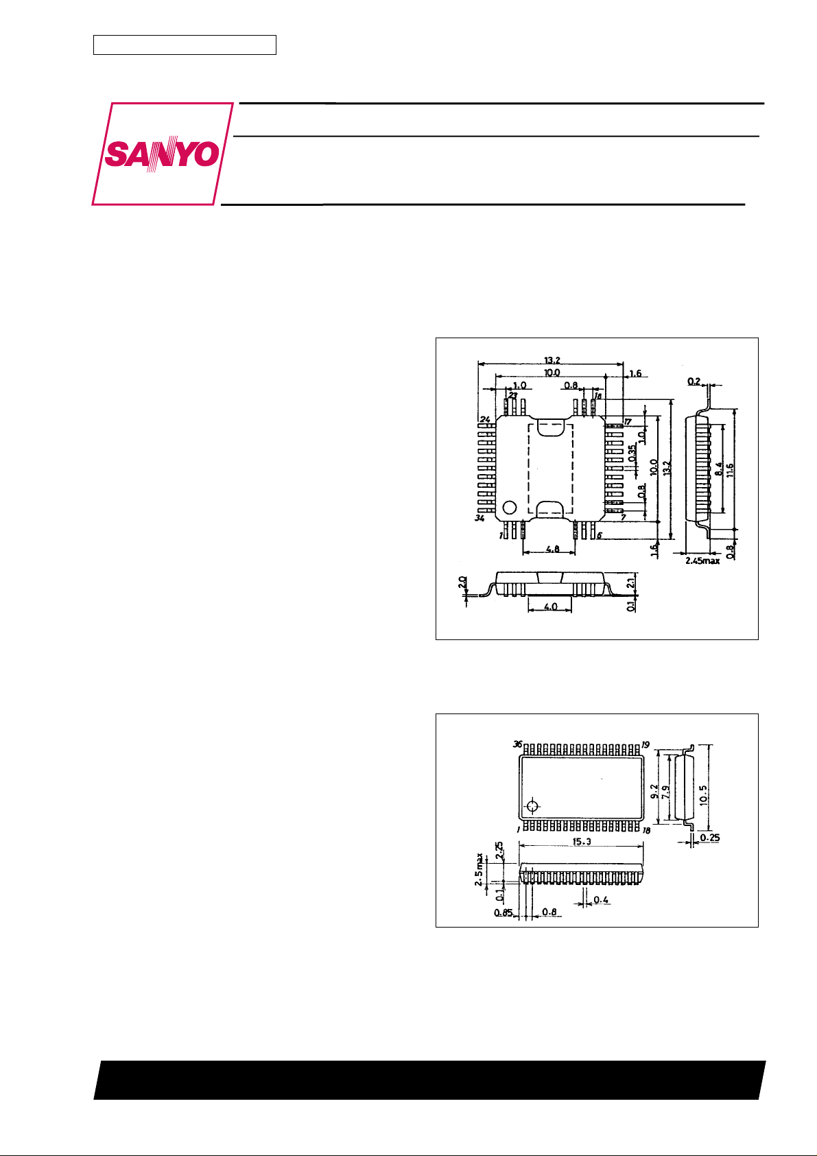
Package Dimensions
unit : mm
3206-QFP34H
[LB1952]
SANYO : QFP34H
3129-MFP36S
[LB1952M]
SANYO : MFP36S
SANYO Electric Co.,Ltd. Semiconductor Bussiness Headquarters
TOKYO OFFICE Tokyo Bldg., 1-10, 1 Chome, Ueno, Taito-ku, TOKYO, 110-8534 JAPAN
92595HA (II) No.5132-1/11
Page 2
LB1952, 1952M
Specifications
Absolute Maximum Ratings atTa=25°C
Parameter Symbol Conditions Ratings Unit
Maximum supply voltage V
Maximum output current I
Allowable power dissipation Pd max
Operating temperature Topr –20 to +75
Storage temperature Tstg –55 to +150
Allowable Operating Ranges atTa=25°C
Parameter Symbol Conditions Ratings Unit
Supply voltage
Hall input amplitude V
GSENSE input range V
max 7V
CC
V
max 24 V
S
max 1.3 A
O
Arbitrarily large heat sink LB1952 12.5 W
Independent IC LB1952 0.77 W
Independent IC LB1952M 0.95 W
V
S
V
CC
HALL
GSENSE
Between Hall inputs ±30 to ±80 mV
Relative to control system GND –0.20 to +0.20 V
5to22 V
4.5 to 5.5 V
C
°
C
°
0-P
Electrical Characteristics atTa=25°C, VCC=5V,VS=15V
Parameter Symbol Conditions min typ max Unit
V
supply current I
CC
CC
[Output]
V
Osat
Output saturation voltage
V
Osat
Output leakage current Ioleak 1.0 mA
[FR]
FR pin input threshold voltage V
FSR
FR pin input bias current Ib (FSR) –5.0 µA
[Control]
CTLREF pin voltage V
CTLREF pin input range V
CREF
CREF
CTL pin input bias current Ib (CTL) With V
CTL pin control start voltage V
CTL
CTL pin control Gm Gm (CTL)
[Current Limit]
LIM current limit offset voltage Voff (LIM)
LIM pin input bias current Ib (LIM)
LIM pin current limit level I lim
[Hall Amplifier]
Hall amplifier input offset
voltage
Voff (HALL) –6 +6 mV
Hall amplifier input bias current Ib (HALL) 1.0 3.0 µA
Hall amplifier common-mode
input voltage
Vcm (HALL) 1.3 3.3 V
[TRC]
Torque ripple correction factor T
RC
ADJ pin voltage Vadj 2.37 2.50 2.63 V
RL= ∞ (when stopped), V
= 500 mA, Rf = 0.5 Ω, Sink + Source
I
O
1
V
CTL=VLIM
= 1.0 A, Rf = 0.5 Ω, Sink + Source
I
O
2
V
CTL=VLIM
= 5 V (with saturation prevention)
= 5 V (with saturation prevention)
CTL
=0V,V
= 0 V 12 18 mA
LIM
2.1 2.6 V
2.6 3.5 V
2.25 2.50 2.75 V
2.05 2.15 2.25 V
IN 1.50 3.50 V
= 5 V, CTLREF : Open 4.0 µA
CTL
With Rf = 0.5 Ω,V
(ST)
Hall input logic fixed, (u, v,w=H,H,L)
With Rf = 0.5 Ω, ∆I
Hall input logic fixed, (u, v,w=H,H,L)
With Rf = 0.5 Ω,V
Hall input logic fixed, (u, v,w=H,H,L)
With V
V
LIM
= 5 V, CTLREF : Open,
CTL
=0V
With Rf = 0.5 Ω,V
Hall input logic fixed, (u, v,w=H,H,L)
At bottom and peak in Rf waveform at IO= 200 mA
(RF=0.5 Ω, ADJ-OPEN) Note 2
=5V,IO^10 mA,
LIM
= 200 mA,
O
=5V,IO^10 mA,
CTL
=5V,V
CTL
LIM
= 2.06 V,
2.00 2.15 2.30 V
0.46 0.58 0.70 A/V
140 200 260 mV
–2.5 µA
830 900 970 mA
9%
Continued on next page.
No.5132 - 2/11
Page 3

LB1952, 1952M
Continued from preceding page.
Parameter Symbol Conditions min typ max Unit
[FG Amplifier]
FG amplifier input offset voltage Voff (FG) –8 +8 mV
FG amplifier input bias current Ib (FG) –100 nA
FG amplifier output saturation
voltage
FG amplifier common-mode
input voltage
[Saturation]
Saturation prevention circuit
lower set voltage
[TSD]
TSD operation temperature T-TSD (Design target) Note 1 180
TSD temperature hysteresis
width
Note 1: No measurements are performed for any values listed in the condition column as design targets.
Note 2: The torque ripple correction factor is calculated using the Rf voltage waveform as follows.
V
(FG) At internal pull-up resistor load on sink side 0.5 V
Osat
V
(FG) 0.5 4.0 V
CM
V
Osat
∆TSD (Design target) Note 1 20
Voltage between each Out and Rf at I
(DET)
Rf = 0.5 Ω,V
CTL=VLIM
=5V
=10mA,
O
0.175 0.25 0.325 V
C
°
C
°
Correction factor =
2 × (Vp − Vb)
Vp + Vb
Truth Table & Control Function
Source → Sink
1
2
3
4
5
6
V→W
W→VL
U→W
W→UL
U→V
V→UL
W→V
V→WL
W→U
U→WL
V→U
U→VL
Hall input
UVW
HHL
HLL
HLH
LLH
LHH
LHL
Hall input logic settings
× 100 (%)
FR
H
H
H
H
H
H
GND level
Note: ‘‘H’’ in the FR column represents a voltage of 2.75V or
more; ‘‘L’’ represents a voltage of 2.25V or less.
(At V
CC
=5V)
Note: ‘‘H’’ in the hall input columns represents a state in which
‘‘+’’ has a potential which is higher by 0.01 V or more
than that of the ‘‘−’’ phase inputs.
Conversely, ‘‘L’’ represents a state in which ‘‘+’’ has a
potential which is lower by 0.01V or more than that of
the ‘‘−’’ phase input.
Note: Since 180° conduction is used as the drive system, other phases than the sink and source phases are turned off.
No.5132 - 3/11
Page 4

LB1952, 1952M
Control Function & Current Limit Function
Control characteristics
Current limit characteristics
Slope = 0.5 A/V typ
Pin Functions
The pin numbers in ( ) are for MFP.
Pin name Pin No. Function
FR 1 (33) Forward/reverse select pin. The pin voltage selects forward/reverse.
GND 2 (34) GND for other than output transistor. Minimum potential of output transistor is at Rf pin.
FGin (–) 5 (3) Input pin when FG amplifier is used with inverted input. Feedback resistor is connected between
FGin (+) 6 (4) Noninverting input pin when FG amplifier is used with differential input. Internal bias is not applied.
FG-OUT 8 (5) FG amplifier output pin. Resistive load provided internally.
CTL 9 (6) Speed controlpin.Controlis exercised by constant-current drive with current feedback appliedfrom
CTLREF 10 (7) Control reference voltage pin. The voltage is set internally to approx. 0.43 x V
LIM 11 (8) Current limiting function control pin. The output current is varied linearly by this pin voltage; slope
FC 12 (9) Speed control loop frequency characteristic correction pin
+
CC
S
, Uin
–
–
–
13, 14 (10, 11)
15, 16 (12, 13)
17, 18 (14, 15)
19 (16) Power supply pin for supplying power to all circuits except output section in IC; this voltage must
22 (21) Output section power supply pin
Uin
Vin+,Vin
Win+, Win
V
V
ADJ 23 (22) Pin for external adjustment of torque ripple correction factor. When this factor is to be adjusted, a
Rf (PWR)
Rf (SNS)
Uout
Vout
Wout
24 (23)
33 (31)
27 (26)
29 (27)
31 (28)
GSENSE 34 (32) GND sensing pin. Byconnecting this pin tothe neighboring GND onthe Rf resistor sideof the motor
(Vth = 2.5 V typ at V
CC
=5V)
this pin and FG-OUT.
Rf. Gm = 0.58 A/V typ at Rf=0.5 Ω
but this can be
varied by applying voltage through a low impedance (input impedance = approx. 4.3 kΩ).
CC
= 0.5 A/V typ at Rf = 0.5 Ω.
U-phase Hall device input pin; logic ‘‘H’’ represent IN+ > IN−.
V-phase Hall device input pin; logic ‘‘H’’ represent IN+ > IN−.
W-phase Hall device input pin; logic ‘‘H’’ represent IN+ > IN−.
be stabilized so as to eliminate ripple and noise.
voltage is externally applied to the ADJ pin through a low impedance. If the voltage applied is
increased, the factor drops; conversely, if it is reduced, the factor rises. The factor varies between
0 and 2 times that of the open state. (The voltage is set to approx. V
impedance is approx. 5 kΩ.)
/2 internally, and the input
CC
Output current detection pin. Current feedback is applied to the control section by connecting Rf
between this pin and GND. The lower oversaturation prevention circuit and torque ripple correction
circuit are activated in accordance with this pin voltage. Since the oversaturation prevention level
is set with this voltage, the lower oversaturation prevention effect may deteriorate in the high
current range if the Rf value is reduced to an extremely low level. The PWR and SENSE pins must
always be connected.
U-phase output pin
V-phase output pin
(Built-in spark killer diode)
W-phase output pin
GND wire which contains Rf, the effect that GND common impedance exerts on Rf can be
eliminated. (This pin must not be left open.)
No.5132 - 4/11
Page 5

Block Diagram
Pin number inside ( ): for MFP
Hall amplifier
LB1952, 1952M
Output stage
Logarithmic
inverse
transformation
& differential
distribution
Hall input combination unit
Control amplifier
Approx. 0.43 × V
Forward/
reverse
selection
(linear matrix)
CC
Combined output
logarithmic compression unit
Differential
distribution &
torque ripple
correction
unit
Upper
saturation
prevention
control
Drive distribution circuit & lower
saturation prevention control
Feedback
amplifier
FG amplifier
Reference
voltage
No.5132 - 5/11
Page 6

Pin Assignment [LB1952]
LB1952, 1952M
(PACKAGE: QFP-34H-A)
Note: FRAME must be connected to GND for GND
potential stabilization.
Pd—Ta
Allowable power dissipation, Pd — W
Ambient temperature, Ta —°C
Top view
No.5132 - 6/11
Page 7

Pin Assignment [LB1952M]
LB1952, 1952M
(PACKAGE: MFP-36S-LF)
Note: Although there is no internal connections between the FRAME pin
and GND, FRAME must be connected to GND externally for GND
potential stabilization.
Pd—Ta
Allowable power dissipation, Pd — W
Ambient temperature, Ta —°C
Top view
No.5132 - 7/11
Page 8

Sample Application Circuit [LB1952]
Forward/reverse instructing voltage
supply pin
Power GND
ADJ voltage supply pin
LB1952, 1952M
Vs
Vcc
Current limit setting voltage
supply pin
CTL REF voltage supply pin
Torque instructing voltage supply pin
Hall output
Hall input
FG output pin
Hall output
Note: The constants provided in this sample application circuit are provided by way of example and are not intended to guarantee the characteristics.
GaAs is
recommended as the
Hall device.
Hall output
Hall bias resistor R is
selected to match the
sensor output.
No.5132 - 8/11
Page 9

Sample Application Circuit [LB1952M]
ADJ voltage supply pin
Forward/reverse instructing
voltage supply pin
Power GND
Vs
LB1952, 1952M
Vcc
Current limit setting voltage supply pin
CTL REF voltage supply pin
Torque instructing voltage supply pin
Hall output
Hall input
FG output pin
Note: The constants provided in this sample application circuit are provided by way of example and are not intended to guarantee the characteristics.
Hall bias resistor R is
selected to match the sensor
output.
GaAs is
recommended as the
Hall device.
Hall output Hall output
No.5132 - 9/11
Page 10

LB1952, 1952M
Pin Input/Output Equivalent Circuit
Pin name Input/Output Equivalent Circuit
Uin (+)
Uin (–)
Vin (+)
Vin (–)
Win (+)
Win (–)
U-OUT
V-OUT
W-OUT
V
S
Rf (POWER)
Rf (SENSE)
Each (+) input
Each output
Each (−) input
Lower oversaturation
prevention circuit input block
CTL
LIM
CTLREF
FR
ADJ
Continued on next page.
No.5132 - 10/11
Page 11

LB1952, 1952M
Continued from preceding page.
Pin name Input/Output Equivalent Circuit
FGin (–)
FGin (+)
FGOUT
FC
No products described or contained herein are intended for use in surgical implants, life-support systems, aerospace equipment,
nuclear power control systems, vehicles, disaster/crime-prevention equipment and the like, the failure of which may directly or
indirectly cause injury, death or property loss.
Anyone purchasing any products described or contained herein for an above-mentioned use shall:
1 Accept full responsibility and indemnify and defend SANYO ELECTRIC CO., LTD., its affiliates, subsidiaries and distributors
and all their officers and employees, jointly and severally, against any and all claims and litigation and all damages, cost and
expenses associated with such use:
2 Not impose any responsibility for any fault or negligence which may be cited in any such claim or litigation on SANYO
ELECTRIC CO., LTD., its affiliates, subsidiaries and distributors or any of their officers and employees jointly or severally.
Information (including circuit diagrams and circuit parameters) herein is for example only; it is not guaranteed for volume
production. SANYO believes information herein is accurate and reliable, but no guarantees are made or implied regarding its use
or any infringements of intellectual property rights or other rights of third parties.
This catalog provides information as of September, 1995. Specifications and information herein are subject to change without notice.
No.5132 - 11/11
 Loading...