

Page 1
Monolithic Digital IC
Ordering number : ENN5340A
N3099TH (OT)/93096HA (OT) No. 5340-1/10
SANYO Electric Co.,Ltd. Semiconductor Company
TOKYO OFFICE Tokyo Bldg., 1-10, 1 Chome, Ueno, Taito-ku, TOKYO, 110-8534 JAPAN
Three-Phase Brushless Sensorless Motor Driver
LB1950V
Overview
The LB1950V is a 3-phase brushless sensorless motor
driver IC that is particularly well-suited to driving
camcorder drum motors.
Features
• Drives 3-phase full-wave brushless sensorless motors
• Soft switching drive
• Speed control using motor power-supply voltage control
for reduced power
• Allows operation from a 3-V power supply.
• The residual output voltage can be set to one of four
values.
• Supports bidirectional rotation.
• Standby function (only the FG and PG amplifiers
operate)
• Brake circuit
• Thermal shutdown circuit
• FG and PG amplifiers
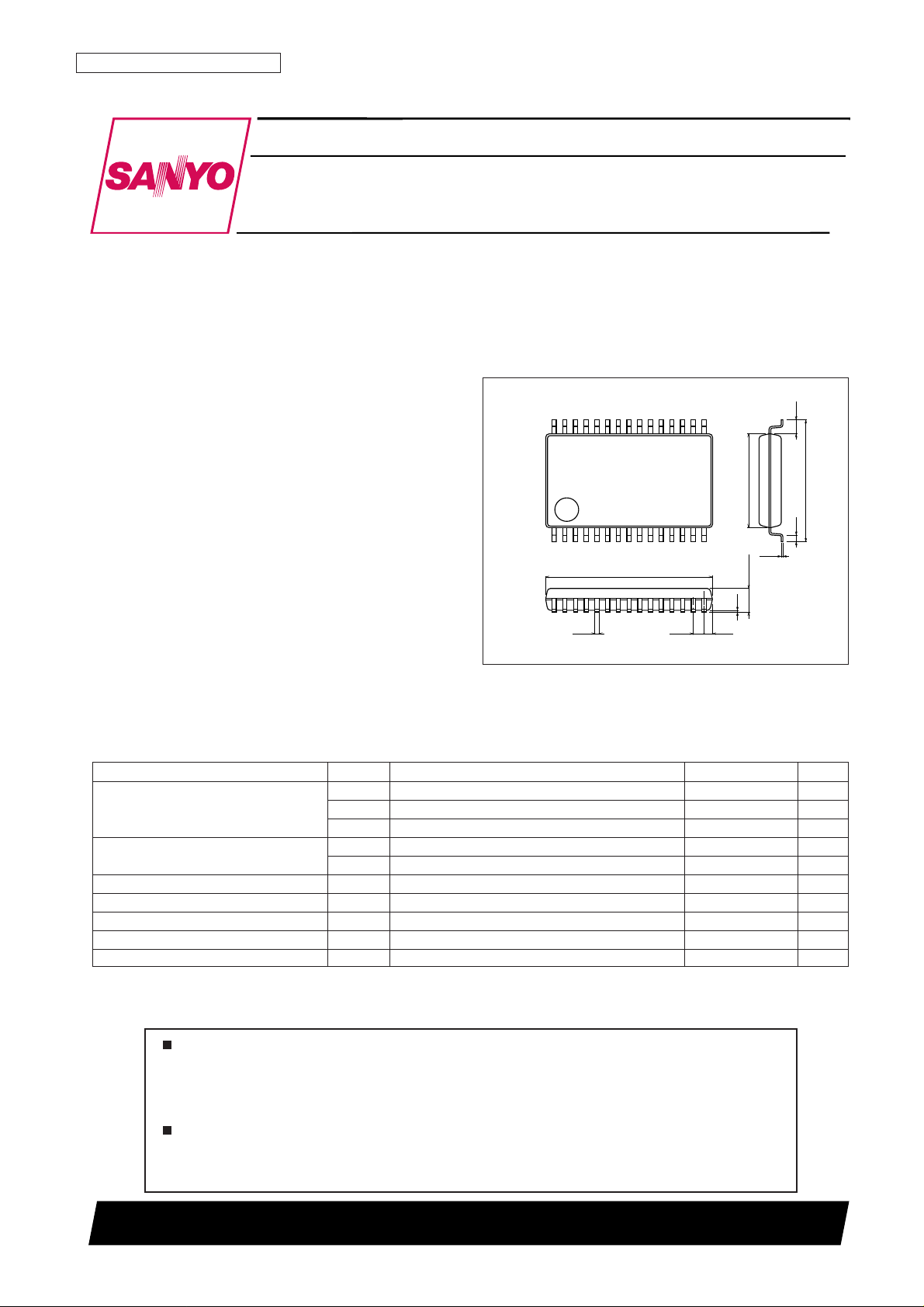
Package Dimensions
unit: mm
3191-SSOP30
115
16
7.6
0.65
9.95
0.5
5.6
0.1
1.6max
1.0
30
0.22
0.43
0.15
[LB1950V]
SANYO: SSOP30
Any and all SANYO products described or contained herein do not have specifications that can handle
applications that require extremely high levels of reliability, such as life-support systems, aircraft’s
control systems, or other applications whose failure can be reasonably expected to result in serious
physical and/or material damage. Consult with your SANYO representative nearest you before using
any SANYO products described or contained herein in such applications.
SANYO assumes no responsibility for equipment failures that result from using products at values that
exceed, even momentarily, rated values (such as maximum ratings, operating condition ranges, or other
parameters) listed in products specifications of any and all SANYO products described or contained
herein.
Specifications
Absolute Maximum Ratings at Ta = 25°C
Parameter Symbol Conditions Ratings Unit
V
CC
1 max 7V
Maximum supply voltage V
CC
2 max 12 V
V
S
max VCC2V
Output voltage
V
O
max VS+ 2 V
V
I
1 max Control system –0.3 to VCC1 + 0.3 V
Input voltage V
I
2 max U, V, W, COM VS+ 2 V
Output current I
O
max 1.0 A
Allowable power dissipation Pd max 0.5 W
Operating temperature Topr –20 to +75 °C
Storage temperature Tstg –55 to +150 °C
Page 2
Allowable Operating Ranges at Ta = 25°C
Electrical Characteristics at Ta = 25°C, VCC1 = 3 V, VCC2 = 4.75 V, VS= 1 V
No. 5340-2/10
LB1950V
Parameter Symbol Conditions Ratings Unit
V
CC
1 2.7 to 6.0 V
Supply voltage V
CC
2 2.7 to 10.0 V
V
S
0 to VCC2V
Parameter Symbol Conditions min typ max Unit
Current drain
I
CC
1IO= 100 mA, RSAT1 = RSAT2 = GND 4.5 7 mA
I
CC
2IO= 100 mA, RSAT1 = RSAT2 = GND 1.2 2.5 mA
I
CC10QVSTBY
= 0 V 1 1.5 mA
Output quiescent current I
CC20QVSTBY
= 0 V 10 µA
I
S30Q
V
STBY
= 0 V 10 µA
Lower side output saturation
V
OU
1IO= 0.1 A, RSAT1 = RSAT2 = open 0.11 V
voltage
V
OU
2IO= 0.4 A, VS= 3 V, RSAT1 = RSAT2 = open 0.33 V
Upper side output saturation
V
OD
1IO= 0.1 A, RSAT1 = RSAT2 = open 0.11 V
voltage
V
OD
2IO= 0.4 A, VS= 3 V, RSAT1 = RSAT2 = open 0.33 V
COM pin common-mode input
V
IC
0.3 VCC2 – 0.9 V
voltage range
Standby pin high-level voltage V
STBYH
2V
CC
1V
Standby pin low-level voltage V
STBYL
–0.2 +0.7 V
Standby pin input current I
STBYIVSTBY
= 3 V 50 µA
Standby pin leakage current I
STBYLVSTBY
= 0 V –10 µA
Brake pin high-level voltage V
BRH
2V
CC
1V
Brake pin low-level voltage V
BRL
–0.2 +0.7 V
Brake pin input current I
BRI
VBR= 3 V 50 µA
Brake pin leakage current I
BRL
VBR= 0 V –10 µA
FRC pin high-level voltage V
FRCH
2V
CC
1V
FRC pin low-level voltage V
FRCL
–0.2 +0.7 V
FRC pin input current I
FRCI
V
FRC
= 3 V 50 µA
FRC pin leakage current I
FRCL
V
FRC
= 0 V –10 µA
Slope pin source current ratio R
SOURCE
ICSLP1SOURCE/ICSLP2SOURCE –12 +12 %
Slope pin sink current ratio R
SINK
ICSLP1SINK/ICSLP2SINK –12 +12 %
CSLP1 source and sink current
R
CSLP1
ICSLP1SOURCE/ICSLP1SINK –35 +15 %
ratios
CSLP2 source and sink current
R
CSLP2
ICSLP2SOURCE/ICSLP2SINK –35 +15 %
ratios
Startup frequency Freq C
OSC
= 0.1 µF, OSC frequency: * 11.5 Hz
Phase delay width Dwidth * 30 deg
Thermal shutdown temperature T
TSD
* 150 180 210 °C
Thermal shutdown hysteresis ∆T
TSD
* 15 °C
[FG Amplifier]
Input offset voltage V
IO
* ±1 ±5 mV
Input bias current I
B
* 250 nA
Common-mode input voltage
V
ICOM
* 12V
range
Output on voltage V
OL
When IO= 10 µA 0.4 V
Output off voltage V
OH
When IO= 10 µA VCC1 – 0.5 V
Schmitt amplifier hysteresis V
SHIS
* 50 mV
Output duty Duty
When the input signal level = 20 mVp-p and the input
30 70 %
frequency = 720 Hz.
Reference voltage V
REF
1.15 1.30 1.45 V
[PG Amplifier]
Input offset voltage V
IO
* ±1 ±5 mV
Input bias current I
B
* 500 nA
Common-mode input voltage
V
ICOM
* 12V
range
Output on voltage V
OL
When IO= 10 µA 0.4 V
Output off voltage V
OH
When IO= 10 µA VCC1 – 0.5 V
Schmitt amplifier hysteresis V
SHIS
* 20 mV
Note: * Items marked with an asterisk are design target values and are not tested.
Page 3
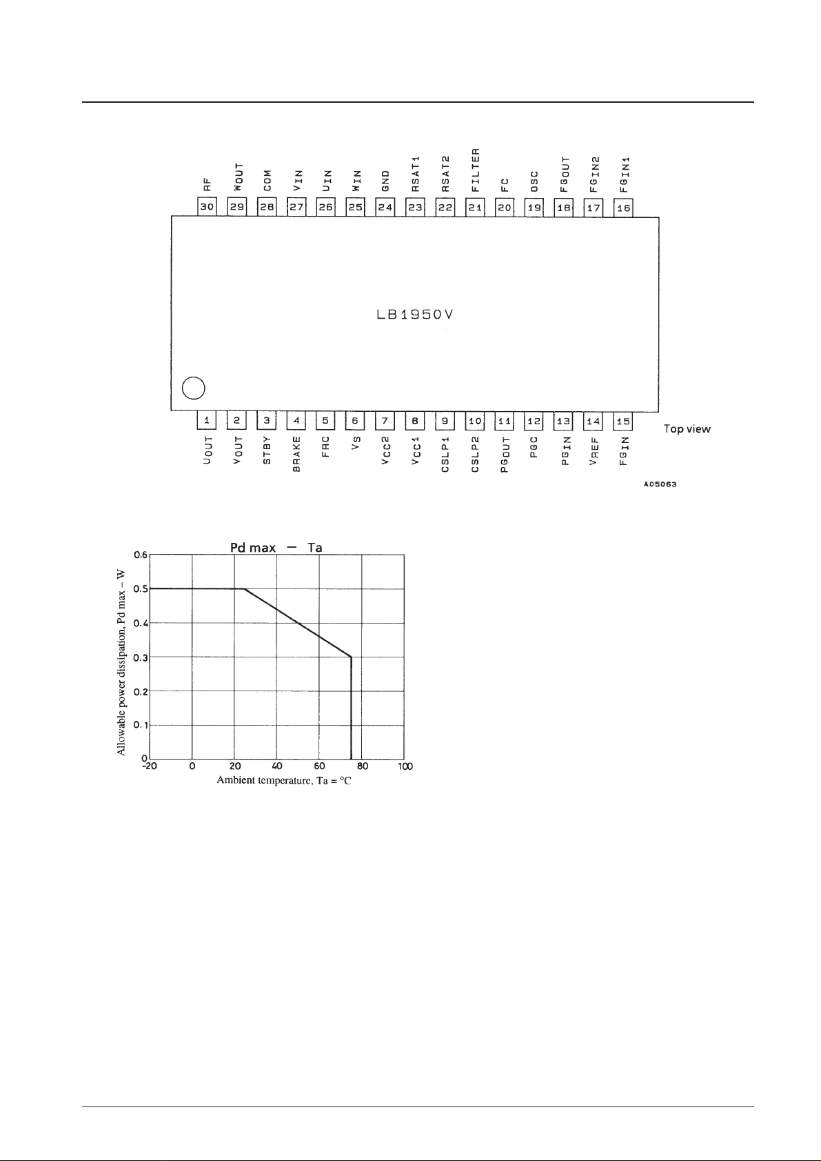
Pin Assignment
No. 5340-3/10
LB1950V
Page 4

Pin Functions
No. 5340-4/10
LB1950V
Pin No. Symbol Pin voltage Equivalent circuit Function
Connection for the triangular wave generator. The coil
output waveform is made to operate in a soft switching
manner by this triangular wave.
CSLP1
CSLP2
9
10
Power supply that provides the voltages other than the
motor voltage, the source side predrive voltage, and the
coil waveform detection comparator voltage.
2.7 to 6 V
V
CC
1
8
Power supply that provides the source side pre-drive
voltage and the coil waveform detection comparator
voltage.
2.7 to 10 V
V
CC
2
7
• Power supply that provides the motor voltage and
determines the output amplitude.
• This voltage must be lower than V
CC
2.
0 V to V
CC
2V
S
6
• Motor forward/reverse switching input
• Low level: forward
(–0.2 to 0.7 V or open)
• High level: reverse
(2 V to V
CC
1)
V
CC
1 max –
0.2 V min
FRC5
• Braking is applied to the motor if a voltage 2.0 V or
higher is applied to this pin.
• This pin must be open or set to a voltage 0.7 V or
lower to set the LB1950V to the motor drive state.
V
CC
1 max –
0.2 V min
BR4
• The LB1950V is set to a mode in which only the FG
and PG amplifiers operate when this pin is open or set
to a voltage 0.7 V or lower.
• This pin must be set to a voltage 2.0 V or higher in the
motor drive state.
V
CC
1 max –
0.2 V min
STBY3
Continued on next page.
Page 5

Continued from preceding page.
No. 5340-5/10
LB1950V
Pin No. Symbol Pin voltage Equivalent circuit Function
Connection for an FG amplifier input signal noise filter
capacitor
FG
IN
2
17
Connection for an FG amplifier input signal noise filter
capacitor
2.0 V max
1.0 V min
(when V
CC
1 =
3 V)
FGIN1
16
FG amplifier input
Connect the FG coil between this pin and V
REF
.
FG
IN
15
• Internal 1.3-V reference voltage
• This voltage is used as the FG and PG amplifier
reference voltage.
V
REF
14
• PG amplifier input
• Connect the PG coil between this pin and V
REF
.
2.0 V max
1.0 V min
(when V
CC
1 =
3 V)
PG
IN
13
Connection for the PG amplifier peak-hold capacitorPGC12
PG amplifier output
PG
OUT
11
Continued on next page.
Page 6

Continued from preceding page.
No. 5340-6/10
LB1950V
Pin No. Symbol Pin voltage Equivalent circuit Function
Ground for all systems other than the output system.GND
24
The residual output voltage setting can be increased by
connecting one, the other, or both of these pins to
ground.
RSAT1
RSAT2
22
23
Connecting a capacitor between this pin and ground
causes the coil output saturation prevention function to
operate. In this state, the motor voltage is controlled by
controlling the VS pin. Also, the torque ripple correction
can be adjusted by changing the value of the external
capacitor.
FILTER21
• Frequency characteristics determination
• Current control system closed loop oscillation can be
stopped by connecting a capacitor between this pin
and ground.
FC20
Connection for the triangular wave oscillator capacitor
that is used to forcibly generate the motor startup
waveform at startup.
OSC19
FG amplifier output
FG
OUT
18
Continued on next page.
Page 7

Continued from preceding page.
No. 5340-7/10
LB1950V
Pin No. Symbol Pin voltage Equivalent circuit Function
• Output transistor ground
• The LB1950V implements fixed-current drive by
detecting the voltage on this pin.
RF30
• W-phase coil output
• U-phase coil output
• V-phase coil output
W
OUT
U
OUT
V
OUT
29
1
2
• Motor coil center tap input
• The LB1950V detects the coil voltage waveform taking
this voltage as the reference.
COM28
Coil waveform detector comparator input
W
IN
U
IN
V
IN
25
26
27
Page 8

Block Diagram
Note: (The values of external components vary depending on the motor used.)
The FG
IN
and PGINpins must be connected to the V
REF
pin if the FG and PG amplifiers are not used.
No. 5340-8/10
LB1950V
Page 9

No. 5340-9/10
LB1950V
Control System Operation
The LB1950V is a current-linear drive motor driver. It implements motor power-supply voltage based speed control by
continually preventing coil output saturation and maintaining the output saturation voltage at the value set by the circuit.
1. The LB1950V detects the sum of the coil output voltage lower side envelope and the diode threshold voltage.
2. The low-pass filter formed by the internal 30-kΩ resistance and the capacitor connected between the FILTER and
GND pins cuts the high-frequency components of the envelope waveform. (The cutoff frequency is 1/2πCR.)
3. The FILTER pin voltage is input to the control amplifier + pin. The reference voltage is input to the control amplifier
– pin, and the control amplifier operates to force the FILTER pin voltage to the same potential as the reference
voltage. The coil output operates in the unsaturated region if this reference voltage is higher than the output transistor
saturation voltage.
4. Also, since the second control amplifier stage controls the RF voltage to a fixed level, the output current (i.e., the RF
current) becomes a fixed current drive.
Supplement: The low-frequency components that are not filtered out by the RC filter on the FILTER pin function to
correct motor torque ripple.
Control System Signals
Page 10

PS No. 5340-10/10
LB1950V
This catalog provides information as of November, 1999. Specifications and information herein are
subject to change without notice.
Specifications of any and all SANYO products described or contained herein stipulate the performance,
characteristics, and functions of the described products in the independent state, and are not guarantees
of the performance, characteristics, and functions of the described products as mounted in the customer’s
products or equipment. To verify symptoms and states that cannot be evaluated in an independent device,
the customer should always evaluate and test devices mounted in the customer’s products or equipment.
SANYO Electric Co., Ltd. strives to supply high-quality high-reliability products. However, any and all
semiconductor products fail with some probability. It is possible that these probabilistic failures could
give rise to accidents or events that could endanger human lives, that could give rise to smoke or fire,
or that could cause damage to other property. When designing equipment, adopt safety measures so
that these kinds of accidents or events cannot occur. Such measures include but are not limited to protective
circuits and error prevention circuits for safe design, redundant design, and structural design.
In the event that any or all SANYO products (including technical data, services) described or contained
herein are controlled under any of applicable local export control laws and regulations, such products must
not be exported without obtaining the export license from the authorities concerned in accordance with the
above law.
No part of this publication may be reproduced or transmitted in any form or by any means, electronic or
mechanical, including photocopying and recording, or any information storage or retrieval system,
or otherwise, without the prior written permission of SANYO Electric Co., Ltd.
Any and all information described or contained herein are subject to change without notice due to
product/technology improvement, etc. When designing equipment, refer to the “Delivery Specification”
for the SANYO product that you intend to use.
Information (including circuit diagrams and circuit parameters) herein is for example only; it is not
guaranteed for volume production. SANYO believes information herein is accurate and reliable, but
no guarantees are made or implied regarding its use or any infringements of intellectual property rights
or other rights of third parties.
 Loading...