

SANYO LB1945H Datasheet
Ordering number : ENN*6193
LB1945H
PWM Current Control Type Stepping Motor Driver
Preliminary
Features
• PWM current control (external excitation)
• Load current digital selection (1–2, W1–2, and 2 phase
excitation drives possible)
• Built-in upper/lower diode
• Simultaneous ON prevention function (feedthrough
current prevention)
• Built-in thermal shutdown circuit
• Built-in noise canceler
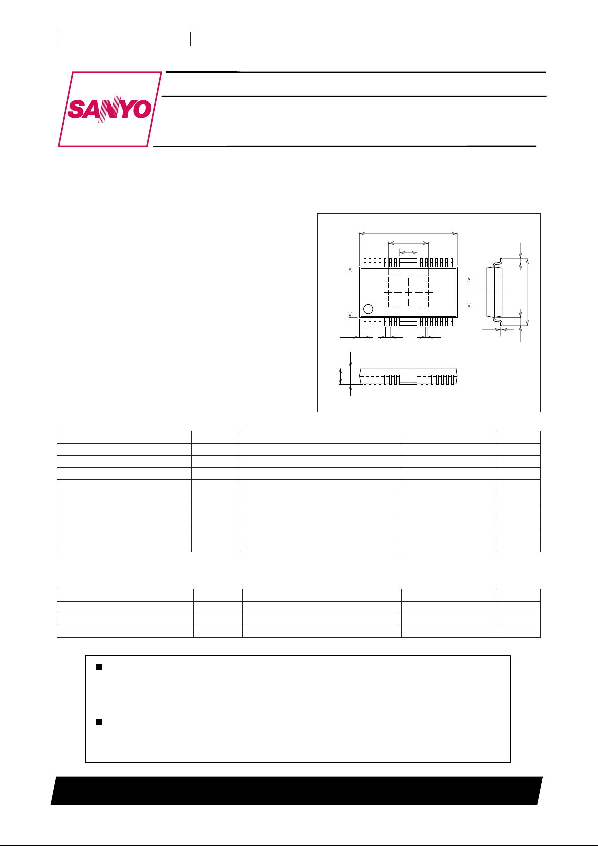
Package Dimensions
unit: mm
3233-HSOP28H
[LB1945H]
15.3
6.2
28 15
7.9
2.7
Monolithic Digital IC
LB1945H
0.65
4.9
10.5
114
0.85
2.25
2.5max
0.1
0.8
0.3
0.25
SANYO : HSOP28H
Specifications
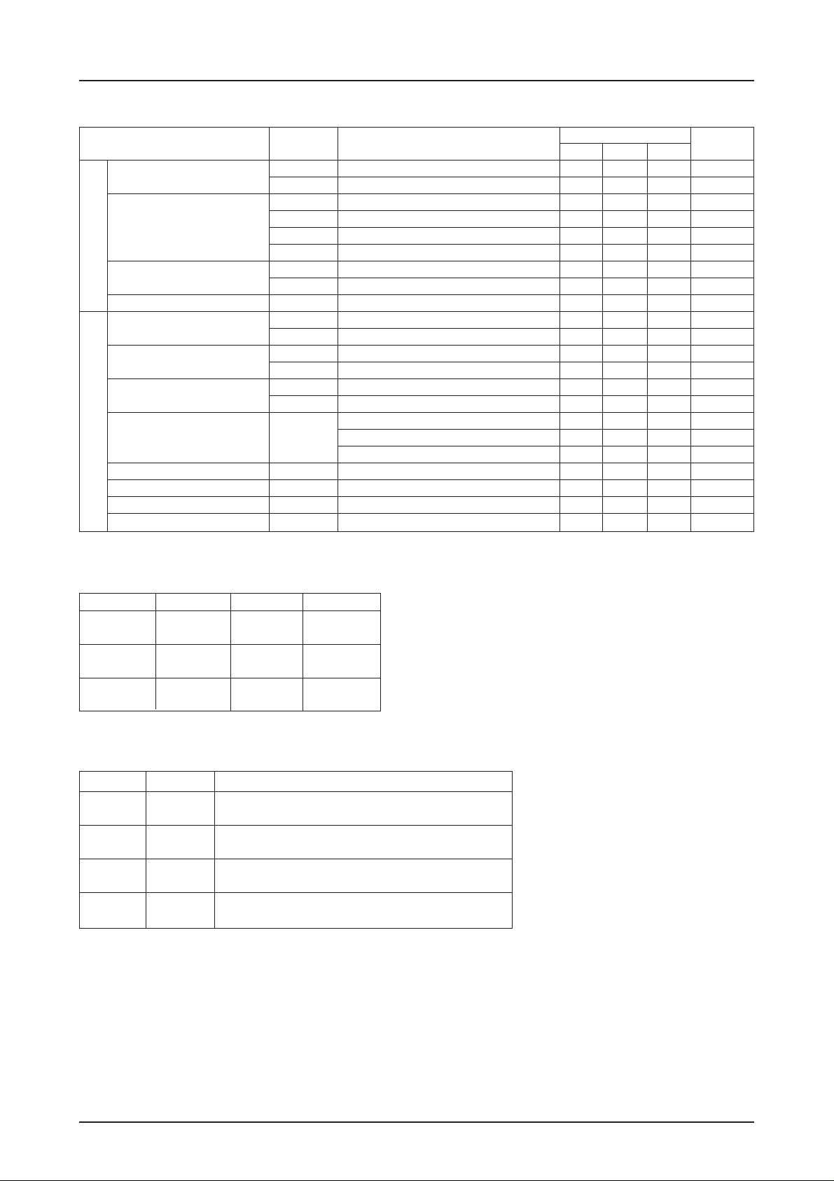
Absolute Maximum Ratings at Ta = 25°C
Parameter Symbol Conditions Ratings Unit
Maximum motor supply voltage VBB max 30 V
Output peak current I OPEAK tw ≤ 20 µs 1.0 A
Output continuous current I O max 0.8 A
Logic supply voltage VCC max 6.0 V
Logic input voltage range VIN max –0.3 to VCC V
Emitter output voltage VE max 1.0 V
Allowable power dissipation Pd max Ta = 25˚C, with specified substrate* 1.9 W
Operating temperature Topr –20 to +90 °C
Storage temperature Tstg –55 to +150 °C
* Specified substrate: 114.3 × 76.1 × 1.6 mm
Allowable Operating Ranges at Ta = 25°C
Parameter Symbol Conditions Ratings Unit
Motor supply voltage VBB 10 to 28 V
Logic supply voltage VCC 4.75 to 5.25 V
Reference voltage VREF 1.5 to 5.0 V
3
, glass epoxy
1.3
Any and all SANYO products described or contained herein do not have specifications that can handle
applications that require extremely high levels of reliability, such as life-support systems, aircraft's
control systems, or other applications whose failure can be reasonably expected to result in serious
physical and/or material damage. Consult with your SANYO representative nearest you before using
any SANYO products described or contained herein in such applications.
SANYO assumes no responsibility for equipment failures that result from using products at values that
exceed, even momentarily, rated values (such as maximum ratings, operating condition ranges, or other
parameters) listed in products specifications of any and all SANYO products described or contained
herein.
SANYO Electric Co.,Ltd. Semiconductor Company
TOKYO OFFICE Tokyo Bldg., 1-10, 1 Chome, Ueno, Taito-ku, TOKYO, 110-8534 JAPAN
82799RM(KI)
No. 6193-1/7
LB1945H
Electrical Characteristics at Ta = 25°C, VBB = 24V, VCC = 5V, VREF = 5.0V
Parameter Symbol Conditions
Output stage supply current I BB ON I1 = 0.8V, I2 = 0.8V, ENABLE = 0.8V 0.5 1.0 2.0 mA
I BB OFF ENABLE = 3.2V 0.2 mA
Output saturation voltage 1 V osat 1 Io = +0.5A sink 0.3 0.5 V
2 V osat 2 Io = +0.8A sink 0.5 0.7 V
3 V osat 3 Io = –0.5A source 1.6 1.8 V
Output Block
Output leakage current I o1(leak) VO = V sink 50 µA
Output sustain voltage V SUS L = 3.9 mH Io = 1.0A *1 30 V
Logic supply current I CC ON I1 = 0.8V, I2 = 0.8V, ENABLE = 0.8V 50.0 70.0 92.0 mA
Input voltage V IH 3.2 V
Input current I IH V IH = 3.2V 35 50 65 µA
Set current control threshold Vref/Vsen I1 = 0.8V, I2 = 0.8V 9.5 10 10.5
value I1 = 3.2V, I2 = 0.8V 13.5 15 16.5
Logic Block
Reference current I ref Vref = 5.0V, I1 = 0.8V, I2 = 0.8V 17.5 25 32.5 µA
CR pin current I CR CR = 1.0V –1.0 mA
Thermal shutdown temperature T TSD 170 °C
Temperature hysteresis width ∆T
*1: Assured design target value, not measured
4 V osat 4 Io = –0.8A source 1.8 2.0 V
I o2(leak) VO = 0V source –50 µA
I CC OFF ENABLE = 3.2V 7.0 10.0 13.0 mA
V IL 0.8 V
I IL V IL = 0.8V 7 10 13 µA
I1 = 0.8V, I2 = 3.2V 25.5 30 34.5
TSD
Ratings
min typ max
40 °C
Unit
Truth Table
ENABLE PHASE OUTA OUTA
LHHL
LLLH
H
I1 I2 Output current
L L Vref / (10 × RE) = IOUT
H L Vref / (15 × RE) = IOUT × 2/3
L H Vref / (30 × RE) = IOUT × 1/3
HH 0
Note: Output is OFF when ENABLE = H or when I1 = I2 = H.
–
OFF OFF
–
No. 6193-2/7
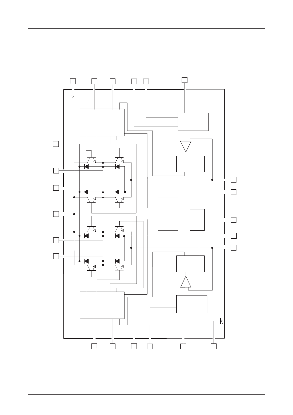
Block Diagram
1
2
7
28 27
8
20
19
17
18
16
23
22
21
65
14
13
11
12
9
10
Control
logic
circuit
Thermal
shutdown
circuit
Current
select
circuit
OSC
Blanking
time
VBB2
24
Current
select
circuit
Control
logic
circuit
Blanking
time
PHASE1
ENABLE2
ENABLE1
IA2
IA1
VBB1
OUTA
OUTB
–
OUTA
–
VCC
PHASE2
IB1
IB2
GND
E2
VREF1
E1
VREF2
CR
OUTB
D-GND D -GND
LB1945H
No. 6193-3/7
 Loading...