

SANYO LB1924 Datasheet
Any and all SANYO products described or contained herein do not have specifications that can handle
applications that require extremely high levels of reliability, such as life-support systems, aircraft’s
control systems, or other applications whose failure can be reasonably expected to result in serious
physical and/or material damage. Consult with your SANYO representative nearest you before using
any SANYO products described or contained herein in such applications.
SANYO assumes no responsibility for equipment failures that result from using products at values that
exceed, even momentarily, rated values (such as maximum ratings, operating condition ranges, or other
parameters) listed in products specifications of any and all SANYO products described or contained
herein.
Ordering number : ENN5687B
73099TH (OT)/83097HA(OT) No. 5687-1/11
Overview
The LB1924 is a direct PWM drive output driver IC
appropriate for the power brushless motors used in office
automation equipment. It includes a speed control circuit,
an FG amplifier, and other peripheral circuits and allows a
drive circuit to be implemented with a single IC. It allows
the number of external components to be reduced by
including a lock protection circuit, a kickback absorption
diode for the lower output side, and other components on
chip.
Functions
• Breakdown voltage: 30 V, output current: 3.1 A
• Direct PWM drive output
• Speed discriminator + PLL speed control technique
• Crystal oscillator circuit
• Built-in FG and integrating amplifiers
• Forward/reverse switching circuit
• Speed lock detection output
• On-chip lower output side kickback absorption diode
• Full complement of built-in protection circuits,
including lock protection, current limiter, and thermal
protection circuits
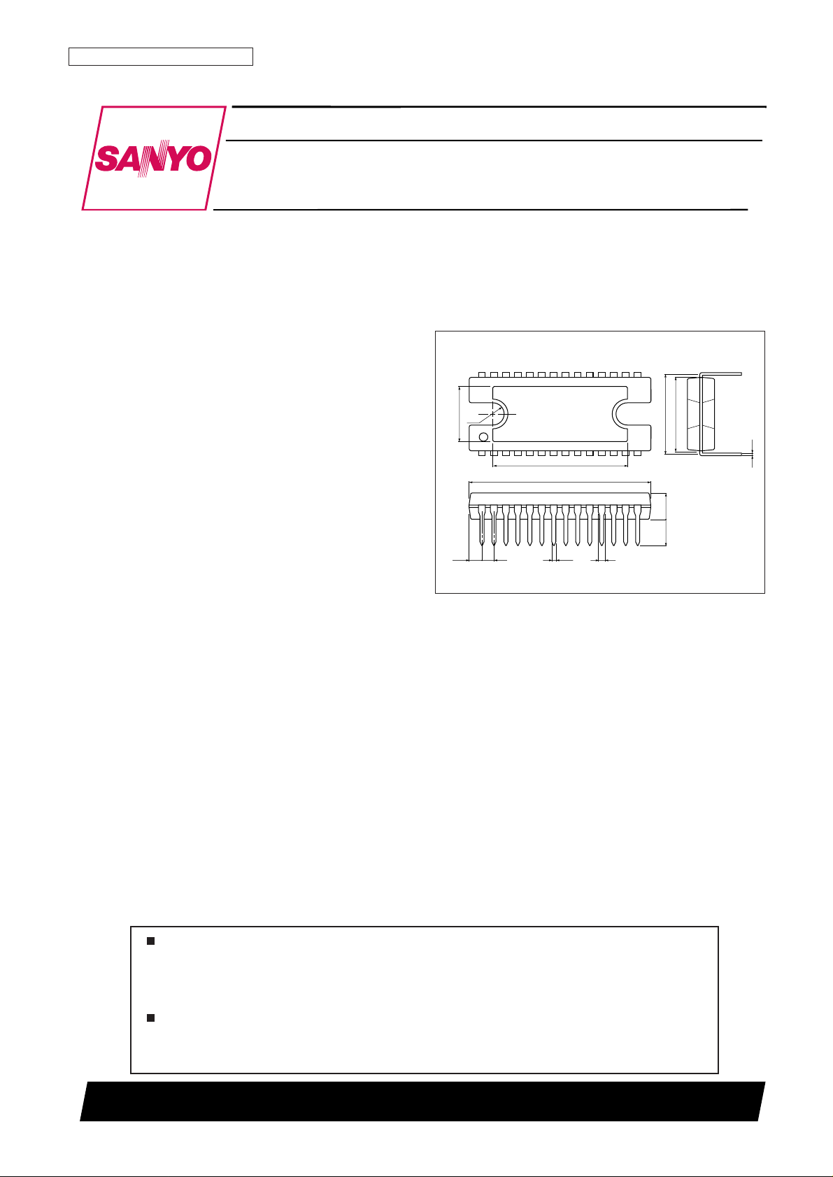
Package Dimension
unit: mm
3147B-DIP28H
1
14
28
15
0.4
0.6
4.04.0
27.0
20.0
R1.7
8.4
1.93 1.78
1.0
12.7
11.2
SANYO: DIP28H
[LB1924]
LB1924
SANYO Electric Co.,Ltd. Semiconductor Company
TOKYO OFFICE Tokyo Bldg., 1-10, 1 Chome, Ueno, Taito-ku, TOKYO, 110-8534 JAPAN
Power Brushless Motor Driver IC for Office
Automation Equipment
Monolithic Digital IC

No. 5687-2/11
LB1924
Parameter Symbol Conditions Ratings Unit
Maximum supply voltage
V
CC
max 30 V
V
M
max VCC≥ V
M
30 V
Output current I
O
max t ≤ 500 ms 3.1 A
Allowable power dissipation
Pd max1 Independent IC 3 W
Pd max2 With an arbitrarily large heat sink 20 W
Operating temperature Topr –20 to +80 °C
Storage temperature Tstg –55 to +150 °C
Specifications
Absolute Maximum Ratings at Ta = 25°C
Parameter Symbol Conditions Ratings Unit
Supply voltage range
V
CC
9.5 to 28 V
V
M
VCC≥ V
M
9 to 28 V
Regulated voltage output current I
REG
0 to –20 mA
Lock detection output current I
LD
0 to 15 mA
Allowable Operating Conditions at Ta = 25°C
Parameter Symbol Conditions
Ratings
Unit
min typ max
Current drain
I
CC
13140mA
I
CC
2 When stopped 5.5 8.0 mA
Output saturated voltage
V
O
sat1 IO= 1A, VO(Sink) + VO(Source) 2.0 2.5 V
V
O
sat2 IO= 2A, VO(Sink) + VO(Source) 2.6 3.2 V
Output leakage current I
O
leak 100 µA
[5-V Regulated Voltage Output]
Output voltage V
REGIO
= –5 mA 4.65 5.00 5.35 V
Line regulation ∆V
REG
1VCC= 9.5 to 28 V 30 100 mV
Load regulation ∆V
REG
2IO= –5 to –20 mA 20 100 mV
[Hall Amplifier]
Input bias current I
HB
–4 –1 µA
Common-mode input voltage range V
ICM
1.5 V
REG
–1.5 V
Hall input sensitivity 60 mVp-p
Hysteresis ∆V
IN
81424mV
Input voltage (low to high) V
SLH
7mV
Input voltage (high to low) V
SHL
–7 mV
[RC Oscillator]
Output high-level voltage V
OH(CR)
2.4 2.7 3.0 V
Output low-level voltage V
OL(CR)
1.1 1.4 1.7 V
Oscillator frequency f
(CR)
R = 22 kΩ, C = 4700 pF 19 kHz
Amplitude V
(CR)
1.0 1.25 1.5 Vp-p
[CROCK Oscillator]
Output high-level voltage V
OH(RK)
2.5 2.8 3.1 V
Output low-level voltage V
OL(RK)
0.5 0.8 1.1 V
External capacitor charging current
I
CHG
1 –10 –8 –6 µA
I
CHG
26810µA
Oscillator frequency f
(RK)
C = 0.047 µF 44 Hz
Amplitude V
(RK)
1.75 1.95 2.25 V
[Current Limiter Operation]
Limiter V
CC-VM
0.45 0.5 0.55 V
[Thermal Shutdown Operation]
Thermal shutdown temperature TSD Design target value (junction temperature) 150 180 °C
Hysteresis ∆TSD Design target value (junction temperature) 40 °C
Electrical Characteristics at Ta = 25°C, VCC= VM= 24 V
Continued on next page.
No. 5687-3/11
LB1924
Parameter Symbol Conditions
Ratings
Unit
min typ max
[FG Amplifier]
Input offset voltage V
IO(FG)
–10 +10 mV
Input bias current I
B(FG)
–1 +1 µA
Output high-level voltage V
OH(FG)IFGO
= –0.2 mA V
REG
–1.2 V
REG
–0.8 V
Output low-level voltage V
OL(FG)IFGO
= 0.2 mA 0.8 1.2 V
FG input sensitivity Gain times 100 3 mV
Schmitt sensitivity for the next stage Design target value 100 180 250 mV
Operating frequency range 2 kHz
Open loop gain f
(FG)
= 2 kHz 45 51 dB
[Speed Discriminator]
Output high-level voltage V
OH(D)IDO
= –0.1 mA V
REG
–1.0 V
REG
–0.7 V
Output low-level voltage V
OL(D)IDO
= 0.1 mA 0.8 1.1 V
Number of counts 512
[PLL Output]
Output high-level voltage V
OH(P)IPO
= –0.1 mA V
REG
–1.8 V
REG
–1.5 V
REG
–1.2 V
Output low-level voltage V
OL(P)IPO
= 0.1 mA 1.2 1.5 1.8 V
[Lock Detector]
Output low-level voltage V
OL(LD)ILD
= 10 mA 0.15 0.5 V
Lock range 6.25 %
[Integrator]
Input bias current I
B(INT)
–0.4 +0.4 µA
Output high-level voltage V
OH(INT)IINTO
= –0.2 mA V
REG
–1.2 V
REG
–0.8 V
Output low-level voltage V
OL(INT)IINTO
= 0.2 mA 0.8 1.2 V
Open-loop gain f (INT) = 1 kHz 45 51 dB
Gain-bandwidth product Design target value 450 kHz
Reference voltage Design target value –5% V
REG
/2 5% V
[Crystal Oscillator]
Operating frequency range f
OSC
1 10 MHz
Low-level pin voltage V
OSCLIOSC
= –0.5 mA 1.7 V
High-level pin current I
OSCHVOSC
= V
OSCL
+0.3 V 0.5 mA
[Start/Stop Pin]
High-level input voltage range V
IH(S/S)
3.5 V
REG
V
Low-level input voltage range V
IL(S/S)
0 1.5 V
Input open voltage V
IO(S/S)
V
REG
–0.5 V
REG
V
Hysteresis ∆V
IN
0.35 0.50 0.65 V
High-level input current I
IH(S/S)V(S/S)
= V
REG
–10 0 +10 µA
Low-level input current I
IL(S/S)V(S/S)
= 0 V –280 –210 µA
[Forward/Reverse Pin]
Output high-level voltage V
IH(F/R)
3.5 V
REG
V
Output low-level voltage V
IL(F/R)
0 1.5 V
Input open voltage V
IO(F/R)
V
REG
–0.5 V
REG
V
Hysteresis ∆V
IN
0.35 0.50 0.65 V
Output high-level voltage I
IH(F/R)V(F/R)
= V
REG
–10 0 +10 µA
Output low-level voltage I
IL(F/R)V(F/R)
= 0 V –280 –210 µA
Continued from preceding page.
No. 5687-4/11
LB1924
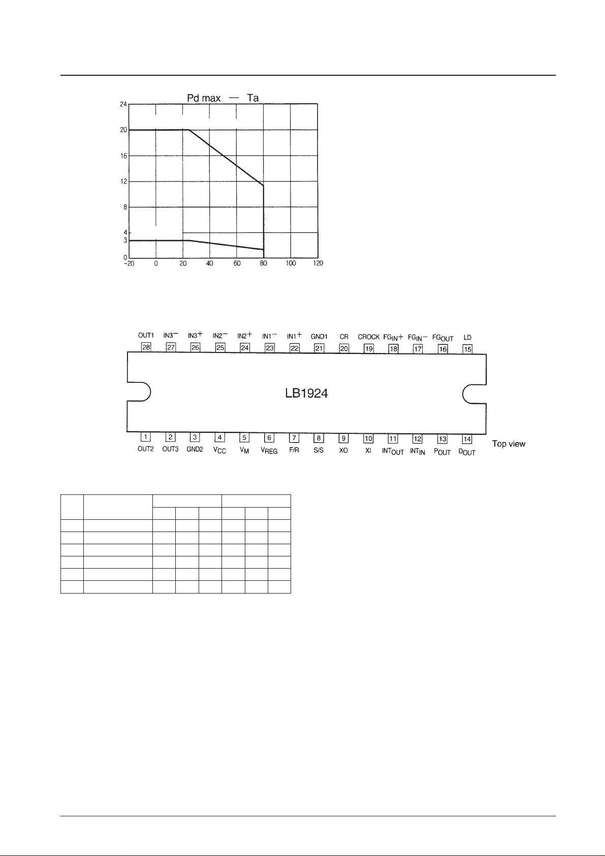
Pin Assignment
Truth Table
Source F/R = L F / R = H
Sink IN 1 IN2 IN 3 IN 1 IN 2 IN 3
1 OUT2 → OUT1 H L H L H L
2 OUT3 → OUT1 H L L L H H
3 OUT3 → OUT2 H H L L L H
4 OUT1 → OUT2 L H L H L H
5 OUT1 → OUT3 L H H H L L
6 OUT2 → OUT3 L L H H H L
Ambient temperature, Ta – °C
Allowable power dissipation, Pdmax – W
Independent IC
With an arbitrarily large heat sink
 Loading...