

Sanyo LB1923M Specifications
63099TH(OT) No. 6067-1/17
SANYO Electric Co.,Ltd. Semiconductor Company
TOKYO OFFICE Tokyo Bldg., 1-10, 1 Chome, Ueno, Taito-ku, TOKYO, 110-8534 JAPAN
Overview
The LB1923M is a pre-driver IC that supports direct
PWM drive and is appropriate for the power brushless
motors used in office automation equipment. A motor
drive circuit with the desired output capability (voltage
and current characteristics) can be constructed by
attaching a driver array at the IC output. The LB1923M
includes on chip a speed control circuit that allows the
motor speed to be varied using an external clock.
Features
• Direct PWM drive output
• Speed discriminator + PLL speed control circuit
• FG and integrating amplifiers
• Forward/reverse switching circuit
• Braking circuit (short braking)
• Speed lock detection output
• Full complement of on-chip protection circuits,
including lock protection, current limiter, and
thermal shutdown protection circuits.
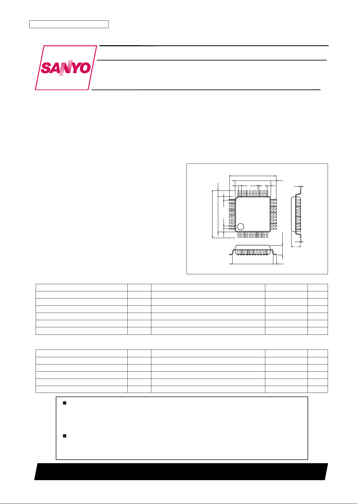
Package Dimensions
unit: mm
3148-QFP44MA
2.8max
0.8
11.6
0.35
10.0
13.2
1.0
1
11
12
22
23
33
34
44
1.0
1.6
0.8
2.5
0.2
0.1
10.0
13.2
1.0
1.0
1.6
0.8
Monolithic Digital IC
Ordering number : EN6067
SANYO: QIP44MA
[LB1923M]
Power Brushless Motor Pre-Driver IC
for OA Equipment
LB1923M
Parameter Symbol Conditions Ratings Unit
Maximum supply voltage V
CC
max 9V
Maximum input current I
REG
max V
REG
pin 10 mA
Output current I
O
max UL, VL, and WL outputs 30 mA
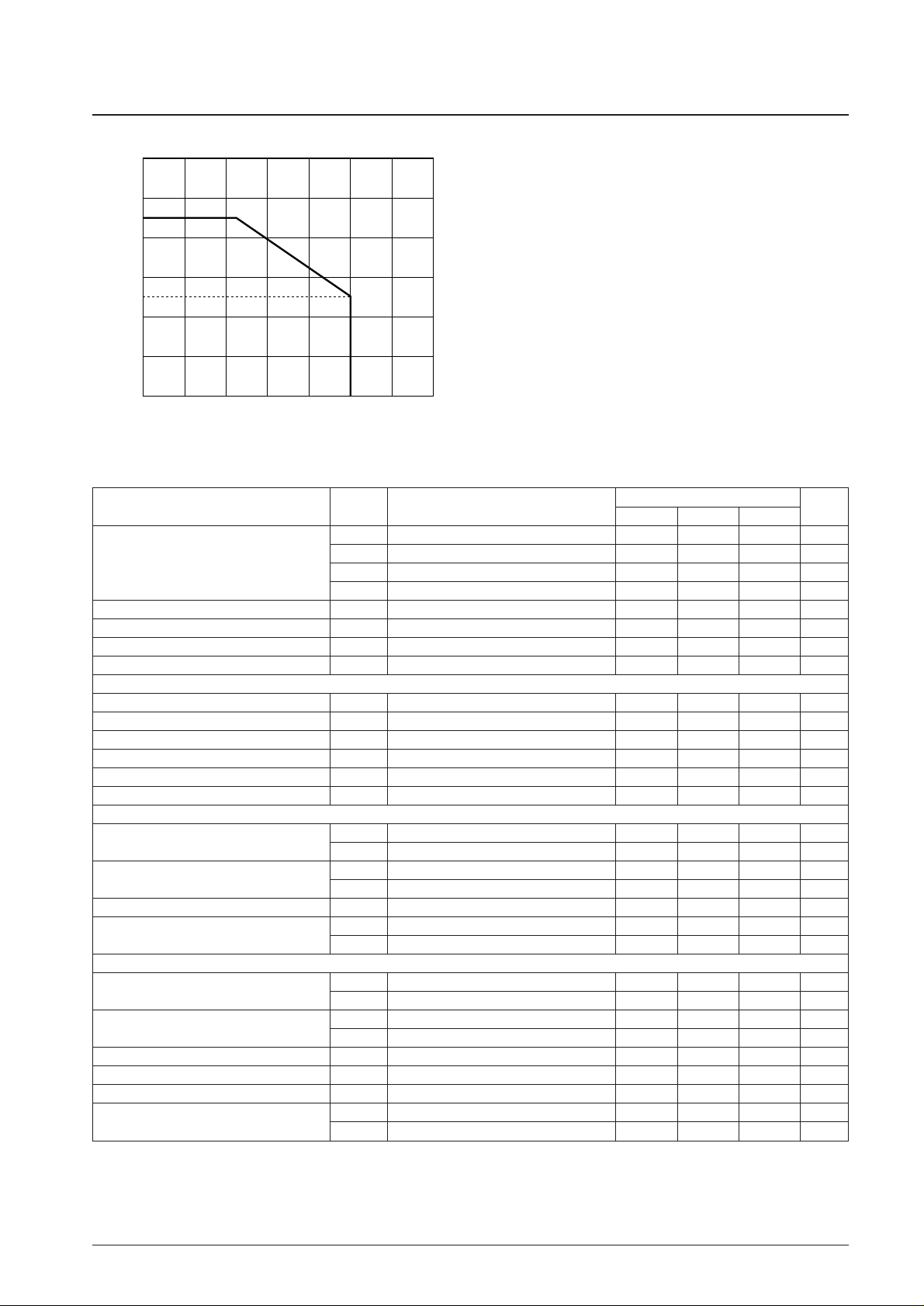
Allowable power dissipation Pd max 0.9 W
Operating temperature Topr –20 to +80 °C
Storage temperature Tstg –55 to +150 °C
Specifications
Absolute Maximum Ratings at Ta = 25°C
Parameter Symbol Conditions Ratings Unit
Supply voltage V
CC
4.4 to 7.0 V
Input current range I
REG
V
REG
pin (7 V) 1 to 5 mA
FG Schmitt output applied voltage V
FGS
0 to 8 V
FG Schmitt output current I
FGS
0 to 5 mA
Lock detection output current I
LD
0 to 20 mA
Allowable Operating Ranges at Ta = 25°C
Any and all SANYO products described or contained herein do not have specifications that can handle
applications that require extremely high levels of reliability, such as life-support systems, aircraft’s
control systems, or other applications whose failure can be reasonably expected to result in serious
physical and/or material damage. Consult with your SANYO representative nearest you before using
any SANYO products described or contained herein in such applications.
SANYO assumes no responsibility for equipment failures that result from using products at values that
exceed, even momentarily, rated values (such as maximum ratings, operating condition ranges, or other
parameters) listed in products specifications of any and all SANYO products described or contained
herein.
No. 6067-2/17
LB1923M
0.2
0
0.4
0.504
0.6
0.8
0.9
1.0
1.2
–20 0 20 40 60 80 120100
Pd max — Ta
Parameter Symbol Conditions
Ratings
Unit
min typ max
I
CC
14260mA
Current drain
I
CC
2 In stop mode 10 20 mA
I
CC
3VCC= 5 V 38 55 mA
I
CC
4VCC= 5 V, In stop mode 8 18 mA
Output saturation voltage V
O
(sat) UL, VL, WL output, IO= 20 mA 0.2 0.7 V
Output current I
O
UH, VH, WH output, V
OUT
= 1.4 V –20 –16 –12 mA
Output leakage current I
O
leak UL, VL, WL output 100 µA
Output off voltage V
O
off UH, VH, WH output 0.5 V
[Hall Amplifier]
Input bias current I
HB(HA)
–4 –1 µA
Common-mode input voltage range V
ICM
1.5 V
CC
– 1.5 V
Hall input sensitivity ∆V
IN(HA)
60 mVp-p
Hysteresis ∆V
IN(HA)
17 32 60 mV
Input voltage low
→ high V
SLH
81630mV
Input voltage high → low V
SHL
–30 –16 –8 mV
[CR Oscillator]
Output high-level voltage
V
OH(CR)
1 3.1 3.4 3.7 V
V
OH(CR)
2VCC= 5 V 2.4 2.7 3.0 V
Output low-level voltage
V
OL(CR)
1 1.5 1.8 2.1 V
V
OL(CR)
2VCC= 5 V 1.1 1.4 1.7 V
Oscillator frequency f
(CR)
R = 75 kΩ, C = 1500 pF 19 kHz
Amplitude
V
(CR)
1 1.4 1.6 1.8 Vp-p
V
(CR)
2VCC= 5 V 1.1 1.3 1.5 Vp-p
[CROCK Oscillator]
Output high-level voltage
V
OH(RK)
1 3.2 3.5 3.8 V
V
OH(RK)
2VCC= 5 V 2.5 2.8 3.1 V
Output low-level voltage
V
OL(RK)
1 0.8 1.1 1.4 V
V
OL(RK)
2VCC= 5 V 0.6 0.9 1.2 V
External capacitor charge current I
CHG
1 –17 –13 –9 µA
External capacitor discharge current I
CHG
2 9 13 17 µA
Oscillator frequency f
(RK)
C = 0.068 µF 35 Hz
Amplitude
V
(RK)
1 2.2 2.4 2.6 Vp-p
V
(RK)
2VCC= 5 V 1.7 1.9 2.1 Vp-p
Electrical Characteristics at Ta = 25°C, VCC= 6.3 V
Continued on next page.
Allowable power dissipation, Pdmax – W
Ambient temperature, Ta – °C
No. 6067-3/17
LB1923M
Parameter Symbol Conditions
Ratings
Unit
min typ max
[VCO Oscillator]
Pin C output high-level voltage
V
OH(C)
1 4.1 4.3 4.6 V
V
OH(C)
2VCC= 5 V 3.2 3.4 3.6 V
Pin C output low-level voltage
V
OL(C)
1 3.6 3.9 4.1 V
V
OL(C)
2VCC= 5 V 2.8 3.0 3.2 V
Oscillator frequency f
(C)
1.0 MHz
Amplitude V
(C)
0.2 0.4 0.6 Vp-p
[Current Limiter Operation]
Limiter V
RF
0.47 0.52 0.57 V
[Thermal Shutdown Operation]
Thermal shutdown operating temperature TSD Design target value 150 180 °C
Hysteresis ∆TSD Design target value 30 °C
[V
REG
Pin]
V
REG
pin voltage V
REG
6.7 7.1 7.4 V
[FG Amplifier]
Input offset voltage V
IO(FG)
–10 +10 mV
Input bias current I
B(FG)
–1 +1 µA
Output high-level voltage V
OH(FG)
VCC– 1.5 VCC– 1 V
Output low-level voltage V
OL(FG)
1 1.5 V
FG input sensitivity Gain: 100× 3mV
Schmitt amplitude for the next stage 100 180 250 mV
Operating frequency range 16 kHz
Open-loop gain f
(FG)
= 2 kHz 45 51 dB
[FGS Output]
Output saturation voltage V
O(FGS)IO(FGS)
= 2 mA 0.1 0.5 V
Output leakage current I
L(FGS)VO
= V
CC
10 µA
[Speed Discriminator Output]
Output high-level voltage V
OH(D)
VCC– 1.0 VCC– 0.7 V
Output low-level voltage V
OL(D)
0.4 1.1 V
[Speed Control PLL Output]
Output high-level voltage
V
OH(P)
1 4.05 4.35 4.65 V
V
OH(P)
2VCC= 5 V 3.25 3.55 3.83 V
Output low-level voltage
V
OL(P)
1 1.85 2.15 2.45 V
V
OL(P)
2VCC= 5 V 1.25 1.55 1.85 V
[VCO PLL Output]
Output high-level voltage V
OH(VCO)
5.3 5.6 V
Output low-level voltage V
OL(VCO)
0.4 11 V
[Lock Detection]
Output saturation voltage V
OL(LD)ILD
= 10 mA 0.1 0.5 V
Output leakage current I
L(LD)VO
= V
CC
10 µA
Lock range –6.25 +6.25 %
[Integrator]
Input offset voltage V
IO(INT)
–10 +10 mV
Input bias current I
B(INT)
–0.4 +0.4 µA
Output high-level voltage V
OH(INT)
VCC– 1.2 VCC– 0.8 V
Output low-level voltage V
OL(INT)
0.8 1.2 V
Open-loop gain 60 dB
Gain-bandwidth product 1.6 MHz
Reference voltage V
B(INT)
–5% VCC/2 5% V
[Filter Amplifier]
Input bias current I
B(FIL)
–0.4 +0.4 µA
Output high-level voltage V
OH(FIL)
VCC– 1.2 VCC– 0.8 V
Output low-level voltage V
OL(FIL)
0.8 1.2 V
Reference voltage
V
B(FIL)
1 –5% 2.0 +5% V
V
B(FIL)
2VCC= 5 V 1.5 1.6 1.7 V
Continued from preceding page.
Continued on next page.
No. 6067-4/17
LB1923M
Parameter Symbol Conditions
Ratings
Unit
min typ max
[S/S Pin]
Output high-level voltage V
OH(S/S)
4.0 V
CC
V
Output low-level voltage V
OL(S/S)
0 1.5 V
Hysteresis
∆V
IN(S/S)
1 0.35 0.45 0.55 V
∆V
IN(S/S)2VCC
= 5 V 0.24 0.34 0.44 V
Pull-up resistance R
U(S/S)
45 63 85 kΩ
[F/R Pin]
Input high-level voltage V
IH(F/R)
4.0 V
CC
V
Input low-level voltage V
IL(F/R)
0 1.5 V
Hysteresis
∆V
IN(F/R)
1 0.35 0.45 0.55 V
∆V
IN(F/R)2VCC
= 5 V 0.24 0.34 0.44 V
Pull-up resistance R
U(F/R)
45 63 85 kΩ
[BR Pin]
Input high-level voltage V
IH(BR)
4.0 V
CC
V
Input low-level voltage V
IL(BR)
0 1.5 V
Hysteresis
∆V
IN(BR)
1 0.35 0.45 0.55 V
∆V
IN(BR)
2VCC= 5 V 0.24 0.34 0.44 V
Pull-up resistance R
U(BR)
45 63 85 kΩ
[CLK Pin]
Input high-level voltage V
IH(CLK)
Design target value 4.0 V
CC
V
Input low-level voltage V
IL(CLK)
Design target value 0 1.5 V
Hysteresis
∆V
IN(CLK)
1 Design target value 0.35 0.45 0.55 V
∆V
IN(CLK)2VCC
= 5 V, Design target value 0.24 0.34 0.44 V
Pull-up resistance R
U(CLK)
45 63 85 kΩ
Input frequency f
(CLK)
16 kHz
[N1 Pin]
Input high-level voltage V
IH(N1)
4.0 V
CC
V
Input low-level voltage V
IL(N1)
0 1.5 V
Hysteresis
∆V
IN(N1)
1 0.35 0.45 0.55 V
∆V
IN(N1)
2VCC= 5 V 0.24 0.34 0.44 V
Pull-up resistance R
U(N1)
45 63 85 kΩ
[N2 Pin]
Input high-level voltage V
IH(N2)
4.0 V
CC
V
Input low-level voltage V
IL(N2)
0 1.5 V
Hysteresis
∆V
IN(N2)
1 0.35 0.45 0.55 V
∆V
IN(N2)
2VCC= 5 V 0.24 0.34 0.44 V
Pull-up resistance R
U(N2)
45 63 85 kΩ
[Low Voltage Protection]
Operating voltage V
SDL
3.75 V
Release voltage V
SDH
4.0 V
Hysteresis ∆V
SD
0.15 0.25 0.35 V
Continued from preceding page.
Speed Discriminator Counts
N1 N2 Number of counts
High or open High or open 64
High or open L 256
L High or open 128
L L 512
No. 6067-5/17
LB1923M
Three-Phase Logic Truth Table (A high (H) input is the state where IN+> IN–.)
Item
F / R = L F / R = H Output
IN1 IN2 IN3 IN1 IN2 IN3 Source Sink
1HLHLHLVHUL
2HLLLHHWHUL
3HHLLLHWHVL
4LHLHLHUHVL
5LHHHLLUHWL
6LLHHHLVHWL
S/S Pin
Pin Assignment
High or open Stop
L Start
BRK Pin
High or open Brake
L Released
CC
WH
V
VREG
34CR
WL
VH
VL
UH
UL
RF
+
–
IN3
IN3
23
24252627282930313233
–
22
IN2
CROCK
(frame) GND
(frame) GND
(frame) GND
FIL
FIL
INT
REF
TOC
35
R
36
37
C
38
39
LB1923M
40
41
O
42
I
43
44
1
234567891011
OUT
INT
IN
INT
OUT
D
OUT
P
LD
BR
F/R
CLK
S/S
N1
N2
21
IN2
20
IN1
19
IN1
18
GND (frame)
17
GND (frame)
16
GND (frame)
FG
15
FG
14
FG
13
12 FGS
+
–
+
–
IN
+
IN
OUT
OUT
Top view
A11831
No. 6067-6/17
LB1923M
Pin Functions
Pin Pin No. Function
IN1+, IN1
–
19, 20
Hall inputs for the phases
IN2+, IN2
–
21, 22
The logic high level corresponds to the state V
IN
+
> V
IN
–
.
IN3+, IN3
– 23, 24
UH 27
VH 29 Outputs. These are fixed-current source outputs.
WH 31
UL 26
The duty is controlled by the output pin PWM.
VL 28
These are open collector sink outputs.
WL 30
V
CC
32 A capacitor must be inserted between this pin and ground to prevent noise entering the circuit.
V
REG
33 7-V shunt regulator output
GND
16 to 18
Ground
38 to 40
CR 34 Used to set the PWM circuit oscillator frequency.
Motor lock protection circuit. Reference signal oscillator connection. Used by the circuit that prevents incorrect
CROCK 35 operation if the clock line is disconnected.
A capacitor must be inserted between this pin and ground.
R 36 VCO circuit. This pin sets the charge and discharge current. A resistor must be inserted between this pin and ground.
C37
VCO oscillator connection. A capacitor must be inserted between this pin and ground. Select a value for that capacitor
such that the C pin oscillator frequency does not exceed 1 MHz.
FIL
I
42 Inverting input to the VCO filter amplifier. This pin is connected to the VCO PLL through an (IC internal) 10-kW resistor.
FIL
O
41 VCO filter amplifier output. This pin is connected to the VCO circuit internally.
D
OUT
3 Speed discriminator output. A low level is output when the motor is over speed.
R
OUT
4 PLL circuit output. Outputs the result of the phase comparison between 1/2fCLK and 1/2fFG.
LD 5
Lock detection output. This is an open collector output.
This pin outputs a low level when the motor speed is within the locked range (±6.25%).
INT
REF
43 Integrating amplifier noninverting input (the 1/2 VCCpotential)
INT
IN
2 Integrating amplifier inverting input
INT
OUT
1 Integrating amplifier output
TOC 44
Torque command input. Normally, this pin is connected to the INTOUT pin. Lowering the TOC pin potential increases
the torque by changing the PWM signal duty for the UL, VL, and WL outputs.
FGIN
+
15 FG amplifier noninverting input (the 1/2 V
CC
potential). A capacitor must be inserted between this pin and ground.
FGIN
–
14 FG amplifier inverting input
FG
OUT
13 FG amplifier output
FGS
OUT
12 FG amplifier (post-Schmitt) output. This is an open collector output.
RF 25
Output current detection. A resistor must be inserted between this pin and ground.
This resistor sets the maximum output current I
OUT
to be 0.5/Rf.
S/S 9 Start/stop control input. Apply a low level for start, and either a high level or an open (high-impedance) state for start.
F/R 7
Forward/reverse control input. Apply a low level for forward, and either a high level or an open (high-impedance) state
for reverse.
BR 6
Braking control input (short braking operation). Apply a low level for start, and either a high level or an open (highimpedance) state to brake the motor.
CLK 8 External clock signal input. 10 kHz max.
N1 10
Speed discriminator count value selection inputs
N2 11
 Loading...