

Page 1
Ordering number : EN4949B
N1595HA (OT)/33195TH (OT) No. 4949-1/10
Applications
• Paper feed and drum motor drivers in FAX and PPC
units
Functions and Features
• The LB1920 is an output current-improved version of
the LB1824
• Three-phase bipolar brushless motor driver
• Digital speed control
• Thermal shutdown circuit
• Start/stop pin provided
• Lock detector output
• Crystal oscillator and divider circuits
• FG and error amplifiers
• Current limiter
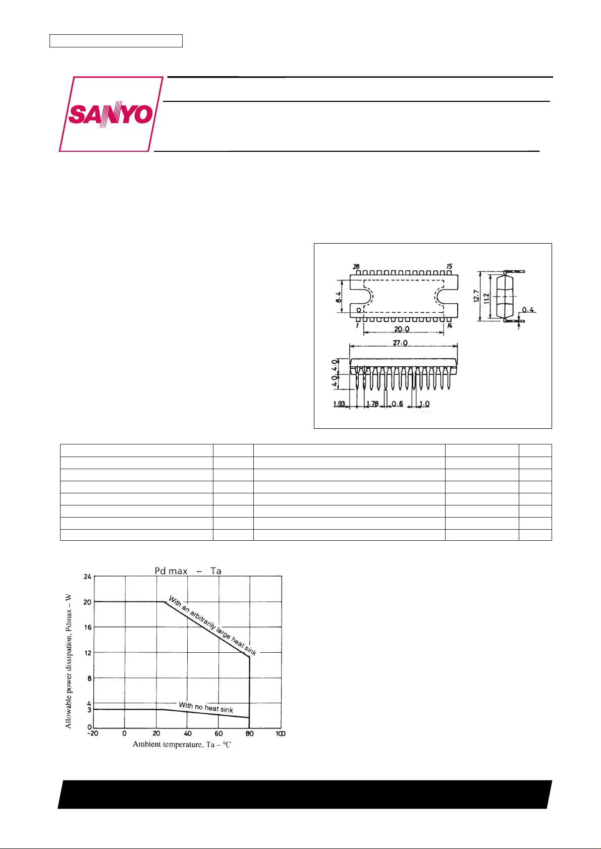
Package Dimensions
unit: mm
3147A-DIP28HS
SANYO: DIP28HS
[LB1920]
LB1920
SANYO Electric Co.,Ltd. Semiconductor Bussiness Headquarters
TOKYO OFFICE Tokyo Bldg., 1-10, 1 Chome, Ueno, Taito-ku, TOKYO, 110-8534 JAPAN
Three-Phase Brushless Motor Driver
for Office Automation Applications
Monolithic Digital IC
Specifications
Absolute Maximum Ratings at Ta = 25°C
Parameter Symbol Conditions Ratings Unit
Maximum supply voltage 1 V
CC
max 30 V
Maximum supply voltage 2 V
M
max 30 V
Output current I
O
max T ≤ 100 ms 3.1 A
Allowable power dissipation 1 Pd max1 Independent IC 3 W
Allowable power dissipation 2 Pd max2 With an arbitrarily large heat sink 20 W
Operating temperature Topr –20 to +80 °C
Storage temperature Tstg –55 to +150 °C
Page 2
Allowable Operating Conditions at Ta = 25°C
Electrical Characteristics at Ta = 25°C, VCC= VM= 24 V
No. 4949-2/10
LB1920
Parameter Symbol Conditions Ratings Unit
Power supply voltage range 1 V
CC
9.5 to 28 V
Power supply voltage range 2 V
M
9 to 28 V
FG Schmitt output supply voltage V
FGS
0 to +8 V
Fixed voltage output current 1 I
O
1 7 V output 0 to –20 mA
Fixed voltage output current 2 I
O
2 5 V output 0 to –20 mA
Fixed voltage output current 3 I
O
3 4 V output 0 to –15 mA
FG Schmitt output current I
FGS
0 to +5 mA
Lock detector output current I
LD
0 to +20 mA
Parameter Symbol Conditions min typ max Unit
Current drain 1 I
CC
1 34 50 mA
Current drain 2 I
CC
2 Stop mode 8 11 mA
Output saturation voltage 1 V
O (sat)
1 IO= 1 A 2.0 3.0 V
Output saturation voltage 2 V
O (sat)
2 IO= 2 A 2.7 4.2 V
Output leakage current I
O leak
100 µA
[7 V Fixed Voltage Output]
Output voltage V
H
IO= –10 mA 6.65 7.0 7.35 V
Voltage variation ∆V
H
1 VCC= 9.5 to 28 V 50 200 mV
Load variation ∆V
H
2 IO= –5 to –20 mA 40 200 mV
[5 V Fixed Voltage Output]
Output voltage V
X
IO= –5 mA 4.45 4.80 5.15 V
Voltage variation ∆V
X
1 VCC= 9.5 to 28 V 50 200 mV
Load variation ∆V
X
2 IO= –5 to –20 mA 5 200 mV
[4 V Fixed Voltage Output]
Output voltage V
FGIO
= –5 mA 3.65 4.0 4.35 V
Voltage variation ∆V
FG
1 VCC= 9.5 to 28 V 40 200 mV
Load variation ∆V
FG
2 IO= –5 to –15 mA 110 200 mV
[Hall Amplifier]
Input bias current I
HB
–4 –1 µA
Common mode input
V
ICM
1.5 5.1 V
voltage range
Hall input sensitivity 60 mVp-p
Hysteresis ∆V
IN
8 14 24 mV
Input voltage low
→ high V
SLH
7 mV
Input voltage high → low V
SHL
–7 mV
[Oscillator]
Output high level voltage V
OH (CR)
2.8 3.1 3.4 V
Output low level voltage V
OL (CR)
0.8 1.1 1.4 V
Oscillator frequency f
(CR)
R = 56 kΩ, C = 1000 pF 15 kHz
Amplitude V
(CR)
2.0 Vp-p
[Current Limiter Operation]
Limiter V
CC-VM
0.4 0.5 0.6 V
[Thermal Shutdown Operation]
Thermal shutdown operating
TSD Design target value 150 180 °C
temperature
Hysteresis ∆TSD 50 °C
Continued on next page.
Page 3
Continued from preceding page.
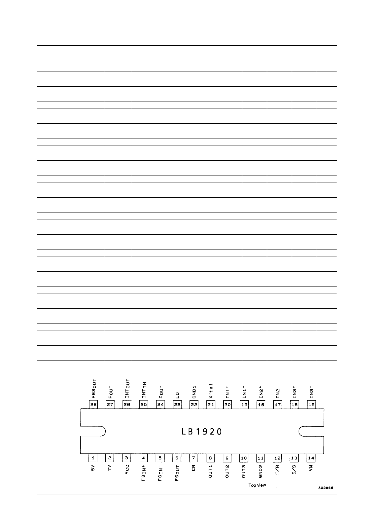
Pin Assignment
No. 4949-3/10
LB1920
Parameter Symbol Conditions min typ max Unit
[FG Amplifier]
Input offset voltage V
IO (FG)
–10 +10 mV
Input bias current I
B (FG)
–1 +1 µA
Output high level voltage V
OH (FG)IFG
= –2 mA 5.5 6 V
Output low level voltage V
OL (FG)IFG
= 2 mA 1 1.5 V
FG input sensitivity Gain: 100 × 3 mV
Schmitt width at next stage 100 180 250 mV
Operating frequency range 2 kHz
Open loop gain f
(FG)
= 2 kHz 45 51 dB
[FGS Output]
Output saturation voltage V
O (FGS)IO (FGS)
= 2 mA 0.1 0.5 V
Output leakage current I
L (FGS)VO
= 5 V 10 µA
[Speed Discriminator]
Output high level voltage V
OH (D)
4.0 4.3 V
Output low level voltage V
OL (D)
0.8 1.1 V
[PLL Output]
Output high level voltage V
OH (P)
3.2 3.5 3.8 V
Output low level voltage V
OL (P)
1.2 1.5 1.8 V
[Counts] 512
[Lock Detector]
Output low level voltage V
OL (LD)ILD
= 10 mA 0.15 0.5 V
Lock range 6.25 %
[Integrator]
Input bias current I
B (INT)
–0.4 +0.4 µA
Output high level voltage V
OH (INT)
3.7 4.3 V
Output low level voltage V
OL (INT)
0.8 1.2 V
Open loop gain 60 dB
Gain bandwidth 1.6 MHz
Reference voltage –5% VX/2 +5% V
[Crystal Oscillator]
Operating frequency range f
OSC
1 10 MHz
[Start/Stop Pin]
Input high level voltage V
IH (S/S)
4.0 V
Input low level voltage V
IL (S/S)
1.5 V
Pull-down resistor R
D (S/S)
30 50 70 kΩ
[Forward/reverse Pin]
Input high level voltage V
IH (F/R)
4.0 V
Input low level voltage V
IL (F/R)
1.5 V
Hysteresis ∆V
IN
0.5 V
Pull-down resistor R
D (F/R)
30 50 70 kΩ
Page 4

Pin Functions
Truth Table
Note: Input high refers to the state where IN+ > IN–.
No. 4949-4/10
LB1920
Pin No. Symbol Function
20, 19 IN1+, IN1– Hall input for OUT1
18, 17 IN2+, IN2– Hall input for OUT2
16, 15 IN3+, IN3– Hall input for OUT3
8 OUT1 Output 1
9 OUT2 Output 2
10 OUT3 Output 3
3 V
CC
Power supply for all blocks other than the output block
14 V
M
Used both as the power supply for the output block as well as for output current detection. The output current can
be converted to a voltage and detected by inserting the resistor Rf between this pin and V
CC
.
22 GND1 Ground for all blocks other than the output block
11 GND2 Output block ground
7 CR PWM oscillator frequency determination
25 INT
IN
Integrator input
26 INT
OUT
Integrator output (speed control)
24 D
OUT
Speed discriminator output
Over speed → high
27 P
OUT
PLL output
23 LD
Lock detector
This pin goes low when the motor speed is within the lock range (±6.25%).
4 FG
IN
+
FG pulse input (4 V power supply)
5 FG
IN
–
FG pulse input
6 FG
OUT
FG amplifier output
28 FGS
OUT
FG amplifier output (after the Schmitt trigger circuit)
21 X’tal Crystal oscillator connection. Connect a crystal oscillator element to this pin.
1 5V 5 V power supply
2 7V 7 V power supply
13 S/S
Start/stop control
Low: start, high: stop
12 F/R
Forward/reverse control
Low: forward, high: reverse
Source → Sink
F/R = low F/R = high
IN1 IN2 IN3 IN1 IN2 IN3
1 OUT3 → OUT2 H H L L L H
2 OUT3 → OUT1 H L L L H H
3 OUT2 → OUT1 H L H L H L
4 OUT2 → OUT3 L L H H H L
5 OUT1 → OUT3 L H H H L L
6 OUT1 → OUT2 L H L H L H
Page 5

The formula below gives the relationship between the oscillator frequency (f
OSC
) and the FG frequency (fFC).
fFC(servo) = f
OSC
/(ECL divisor (16) × number of counts)
= f
OSC
/8192
Crystal Oscillator External Circuit
Equivalent Circuit Block Diagram
No. 4949-5/10
LB1920
External Circuit Constants (reference values)
Note: However, the crystal used must have a fundamental frequency fo
impedance to 3fo impedance ratio of 1:5 or greater.
X’tal (MHz) C1 (pF) C2 (pF) R (kΩ)
3 to 4 39 82 0.82
4 to 5 39 82 1.0
5 to 7 39 47 1.5
7 to 10 39 27 2.0
Page 6

Sample Application Circuit
AC Test Circuit Diagram
No. 4949-6/10
LB1920
Page 7

This section describes the LB1920 and the external components used.
1. Speed Control Circuit
This IC uses the combination of a speed discriminator circuit and a PLL circuit for speed control. The speed
discriminator circuit outputs an error signal once every two FG periods using a charge pump scheme. The PLL
circuit outputs a phase error signal once every FG period, also using a charge pump scheme. As compared to earlier
schemes that only used a speed discriminator, the combination of a PLL circuit with a speed discriminator provides
improved speed variation suppression when using a motor with large load variations. Since the following formula
determines the FG servo frequency, the motor speed must be set using the number of FG pulses and the crystal
oscillator frequency.
fFG(servo) = f
OSC
/8192
f
OSC
: crystal oscillator frequency
2. Direct PWM Drive
This IC adopts a direct PWM drive scheme to minimize power loss in the output. The output transistors are always
saturated when on and the motor drive power is adjusted by changing the output on duty. Since output switching is
performed by the lower side transistor, the three Schottky diodes D1, D2 and D3 must be inserted between OUT and
VCC. (Note that a through current will flow at the instant the lower side transistor turns on if these diodes do not have
a short reverse recovery time.) Normal rectifying diodes can be used for the diodes between OUT and ground.
3. Current Control Circuit
The current control circuit applies current control at a current determined by the relation I = 0.5/Rf, i.e. peak current
limitation. The control operation reduces the output on duty and thus suppresses the current. No phase compensation
capacitor is required.
4. Speed Lock Range
The speed lock range is ±6.25% of the fixed speed and the LD pin goes low when the motor is in the lock range.
(This pin is an open collector output.) When the motor speed goes out of the lock range, the LB1920 changes the
motor drive output on duty according to the speed error to control the motor speed to be within the lock range.
5. PWM Frequency
The PWM frequency is determined by the resistor and capacitor (R3 and C6) connected to the CR pin.
• When R3 is connected to the 4 V fixed voltage supply
f
PWM
≈ 1/(1.2 × C × R)
• When R3 is connected to the 7 V fixed voltage supply
f
PWM
≈ 1/(0.5 × C × R)
R3 should not be any smaller than 30 kΩ. A PWM frequency of about 15 kHz is desirable. If the PWM frequency is
too low, the motor will vibrate at the PWM frequency when the motor is restrained causing disturbing audible noise.
Inversely, switching loss increases if the PWM frequency is too high.
6. Ground Leading
GND1 (pin 22) is the ground for circuits other than the output block.
GND2 (pin 11) is the ground for the output block (emitters of the sink transistors).
D4, D5 and D6 are connected to GND2. All other external components are connected to GND1. The GND1 and
GND2 lines are connected to a single ground point at the connector. Since GND2 carries large currents, it should be
kept as short as possible.
7. Output Parasitic Effects
Parasitic effects occur when the output pin voltage falls –0.7 V (this value decreases as the temperature increases)
below the GND1 and GND2 voltage. Similarly, the output pin voltage should not be allowed to exceed VCCby more
than 1 V. When parasitism occurs, initially speed control is lost intermittently, but if the amount of parasitism
increases the output transistors can be destroyed. Schottky diodes with a small Vfare used for D1, D2 and D3 to
prevent through currents. As a result, the potential difference between the output pins and VCCis not that much of a
problem. Although normal rectifying diodes can be used for D4, D5 and D6, the printed circuit board pattern must be
kept as short as possible (as recommended in item 6) to prevent parasitism from occurring.
No. 4949-7/10
LB1920
Page 8

8. External Interface Pins
• LD pin
Output type: open collector
Breakdown voltage: Maximum supply voltage of 30 V
Saturation voltage sample-to-sample variation (reference value) (ILD= 10 mA)
0.10 to 0.15 V
• FGS pin
Output type: open collector
Breakdown voltage: Maximum supply voltage of 30 V
Saturation voltage sample-to-sample variation (reference value) (I
FGS
= 2 mA)
0.12 to 0.18 V
The FGS pin outputs the FGS amplifier output converted to a pulse output by a hysteresis comparator for use in
speed monitoring. The pull-up resistor is not required when this pin is not used.
• Start/stop pin
Input type: pnp transistor base with a 50 kΩ pull-down resistor to ground.
Threshold level (typical): about 2.6 V
In stop mode, the 4, 5 and 7 V fixed voltage power supplies are turned off.
• F/R pin
Input type: pnp transistor base with a 50 kΩ pull-down resistor to ground.
Threshold level (typical): about 2.2 V (high to low), about 2.7 V (low to high)
Hysteresis: about 0.5 V
F/R switching must be done when stopped.
9. Fixed Voltage Power Supply Temperature Characteristics
• 4 V power supply: about –0.5 mV/°C (typical)
• 5 V power supply: about –0.6 mV/°C (typical)
• 7 V power supply: about –2.5 mV/°C (typical)
10. FG Amplifier
The resistors R1 and R2 set the FG amplifier gain, with the gain being determined by the formula G = R2/R1. The
capacitors C4 and C5 determine the FG amplifier frequency characteristics, with R1 and C4 forming a high-pass
filter and R2 and C5 forming a low-pass filter. Since the FG amplifier is followed by a Schmitt comparator, the
values of R1, R2, C4 and C5 must be set up so that FG amplifier output is over 250 mVp-p. In particular, it is
desirable that the FG amplifier output be set up to be between 1 and 3 V during steady-state rotation.
11. External Capacitors
• C3
The capacitor C3 is required for FGIN+ pin fixed voltage power supply stabilization and IC internal logic initial
reset pulse generation. Although the value of this capacitor can be quite small for power supply stabilization, a
relatively large capacitance (about 4.7 µF) is required for reset pulse generation. The reset pulse is generated during
the time the FGIN+ pin goes from 0 to about 1.3 V. If the reset does not operate, LD will turn on briefly at startup.
If this phenomenon is not a problem, a capacitor of about 0.1 µF can be used for C3. After C3 is charged to 4 V,
when VCCis turned off (or the motor is stopped), the charge on C3 is discharged through the IC internal resistance
to ground, which is about 10 kΩ.
• C1 and C2
The capacitors C1 and C2 are required for fixed voltage power supply stabilization. Since this IC adopts a direct
PWM drive scheme and switches large currents in the output, noise can occur easily. Thus the power supply must
be adequately stabilized so that this noise does not cause the IC to operate incorrectly. C1, C2 and C3 must be
connected as close as possible to GND1. In particular, C1’s characteristics are easily influenced and thus requires
caution.
No. 4949-8/10
LB1920
Page 9

12. External Resistors
• R4 and R5
The resistors R4 and R5 exist to apply the F/R pin high level input. Since the F/R input has a pull-down resistor of
about 50 kΩ, it is at the low level when open. Apply a voltage of over 4.0 V and under 6.3 V to input a high level.
• R15
The resistor R15 exists to apply the S/S pin high level input. Since the S/S input has a pull-down resistor of about
50 kΩ, it is at the low level when open. Apply a voltage of over 4.0 V and under 6.3 V for the start state high level
input. Although dividing the voltage with two resistors, as is done with the F/R input, would improve the resistance
to noise since a lower input impedance can be set up, when noise is not a problem the high level can be set by
connecting a single resistor such as R15. A value of 180 kΩ is recommended.
If VCCrises slowly (less than about 10 V/ms) when power is first applied, the motor may rotate somewhat. This is
because the S/S pin input voltage is resistor divided and the input voltage will be under 2.5 V (the start input level)
when VCCis under 12 V. If the rise rate cannot be increased and this phenomenon is a problem, it can be resolved
by connecting a capacitor between VCCand the S/S pin.
13. Through Currents due to the Direct PWM Scheme
In the direct PWM scheme, through currents flow in the outputs due to transistor switching (in applications
implemented with either discrete components or the LB1822.) This is due to output transistor delays and parasitic
capacitances. Previously, when this was a problem, additional capacitors were used to resolve the problem. However,
since the LB1920 resolves this problem at the circuit level, no additional external components are required. During
switching, whiskers of less than about 10 ns can be observed on the RF voltage waveform, but these are not a
problem.
14. Oscillator Element
Normally, a crystal oscillator is used with this IC. If the speed control characteristic requirements are not stringent, a
ceramic oscillator could be used. To avoid problems, consult the manufacturer of the oscillator element when
selecting the oscillator element and determining the values of the external resistors and capacitors.
15. Sample IC Internal Power Dissipation Calculation (calculated for VCC= 24 V and typical rated values)
• Power dissipation due to current drain (ICC)
Start mode:
P1 = VCC× ICC1 = 24 × 34 m = 0.82 W
Stop mode:
P2 = VCC× ICC2 = 24 × 8 m = 0.19 W
• Power dissipation when –10 mA is drawn from the 7 V fixed voltage power supply
P3 = (VCC– 7) × 10 m= 17 × 10 m = 0.17 W
• Power dissipation due to output drive current (when the output on duty is 100%)
P4 ={(VCC– 1)2/8 k} + {(VCC– 2)2/10 k}
= (232/8 k) + (222/10 k) = 0.12 W
• Power dissipation in the output drive transistors (when IO= 2 A and the output on duty is 100%)
P5 = V
Osat
2 × IO= 2.7 × 2 = 5.4 W
Therefore, the total power dissipation for the whole IC is:
In stop mode:
P = P2 = 0.19 W
In start mode:
P = P1 + P3 + P4 + P5 = 6.51 W
(For a output on duty of 100%)
16. IC Temperature Rise Measurement Techniques
• Thermocouple measurement
Attach the thermocouple to a fin on the heat sink when using a thermocouple to measure the IC temperature. This
technique is simple but is subject to large measurement errors when the heat generation is not consistent.
• Measurement using IC internal diode characteristics
We recommend using the parasitic diode that exists between the INT.IN and ground in this IC. (According to
Sanyo data, the temperature characteristic of this diode is about 1.8 mV/°C for ID= 1 mA.) The external resistor
must be removed during testing.
No. 4949-9/10
LB1920
Page 10

PS No. 4949-10/10
LB1920
17. Servo Constants
Since the servo constant calculation depends strongly on the motor characters and requires significant expertise, we
recommend that the motor manufacturer determine the constants in normal cases. Sanyo can provide the required IC
characteristics data for the servo constant calculations and frequency characteristics simulation data for the filter
characteristics specified by the motor manufacturer.
When the resistor (R10) inserted between DOUT and INT.IN is too small, C8 and C9 will become too large and if
R10 is too large speed errors become more likely to occur due to the speed discriminator cutoff and the integrator
input current. Therefore, a value of between 10 kΩ and 100 kΩ is advisable. If the resistor (R8) inserted between
POUT and INT.IN is too small, the influence of the PLL system will be too large and pull-in to synchronization with
the lock state will degrade. Therefore, this resistor must not be too small. We recommend a value of around 1 MΩ
when R10 is 75 kΩ. First determine the constants for the speed discriminator (R9, R10, C8 and C9) and then
determine the value of R8 in the PLL system.
This catalog provide information as of November, 1995. Specifications and information herein are subject to
change without notice.
■ No products described or contained herein are intended for use in surgical implants, life-support systems, aerospace
equipment, nuclear power control systems, vehicles, disaster/crime-prevention equipment and the like, the failure of
which may directly or indirectly cause injury, death or property loss.
■ Anyone purchasing any products described or contained herein for an above-mentioned use shall:
➀ Accept full responsibility and indemnify and defend SANYO ELECTRIC CO., LTD., its affiliates, subsidiaries and
distributors and all their officers and employees, jointly and severally, against any and all claims and litigation and all
damages, cost and expenses associated with such use:
➁ Not impose any responsibility for any fault or negligence which may be cited in any such claim or litigation on
SANYO ELECTRIC CO., LTD., its affiliates, subsidiaries and distributors or any of their officers and employees
jointly or severally.
■ Information (including circuit diagrams and circuit parameters) herein is for example only; it is not guaranteed for
volume production. SANYO believes information herein is accurate and reliable, but no guarantees are made or implied
regarding its use or any infringements of intellectual property rights or other rights of third parties.
 Loading...