SANYO LB1916 Datasheet

Ordering number : EN5653
53197HA(OT) No. 5653-1/7
Overview
The LB1916 is a 3-phase motor driver that is optimal for
driving CD-ROM spindle motors.
Functions and Features
• 3-phase brushless motor driver
• 120° voltage linear drive control
• V-type input used for the control voltage
• Control gain switching supported
• Pins for system control and control of acceleration and
deceleration provided.
• Start/stop pin provided.
• Hall bias circuit
Package Dimensions
unit: mm
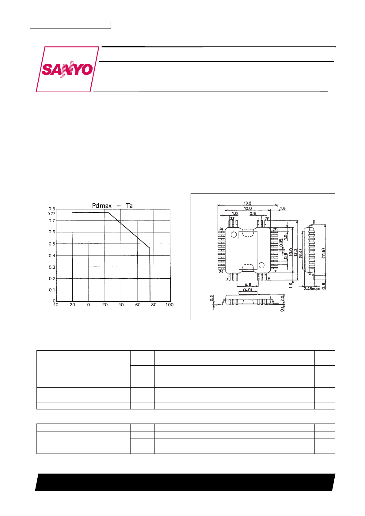
3219-QFP34H-C
SANYO: QFP34H-C
[LB1916]
LB1916
SANYO Electric Co.,Ltd. Semiconductor Bussiness Headquarters
TOKYO OFFICE Tokyo Bldg., 1-10, 1 Chome, Ueno, Taito-ku, TOKYO, 110 JAPAN
CD-ROM Spindle Motor Driver
Monolithic Digital IC
Ambient temperature, Ta – °C
Allowable power dissipation, Pdmax – W
Parameter Symbol Conditions Ratings Unit
Maximum supply voltage
V
CC
1 max 14 V
V
CC
2 max 7.0 V
Output voltage V
O
U, V, W 13 V
Output current I
OUT
1.0 A
Allowable power dissipation Pd max Independent IC 0.77 W
Operating temperature Topr –20 to +75 °C
Storage temperature Tstg –55 to +150 °C
Specifications
Absolute Maximum Ratings at Ta = 25°C
Parameter Symbol Conditions Ratings Unit
Supply voltage
V
CC
1 5 to 12.5 V
V
CC
2VCC1 ≥ VCC2 4.3 to 6.5 V
V
CREF
input voltage V
CREF
VCC2/2±1.0 V
Allowable Operating Ranges at Ta = 25°C

No. 5653-2/7
LB1916
Parameter Symbol Conditions
Ratings
Unit
min typ max
I
CC
1
V
C
= 2.5 V, V
CREF
= 2.5 V, RL= ∞,
17 30 mA
Supply current drain
VS/S = 5 V, VRF = GND
I
CC
2 VC= 2.5 V, V
CREF
= 2.5 V 7.5 10.5 mA
(I
CC
for VCC1) ICC3
V
C
= 2.5 V, V
CREF
= 2.5 V, RL= ∞,
0.9 3 mA
VS/S = 0 V, VRF = GND
[Drive Block]
Output saturation voltage
V
O
(sat)1 I
OUT
= 0.4 A, sink + source 1.6 2.2 V
V
O
(sat)2 I
OUT
= 0.8 A, sink + source 2.0 3.0 V
Output TRS sustainable voltage V
O
(sus) I
OUT
= 20 mA, * 14 V
Output center voltage V
OQ
VC= 2.5 V, V
CREF
= 2.5 V 5.7 6.0 6.3 V
Hall amplifier input offset voltage VH offset –5 +5 mV
Hall amplifier input bias current IH bias 1 5 µA
Hall amplifier common-mode input voltage range
VHch 1.3 2.2 V
Hall input/output voltage gain VG
HO
38 41 44 dB
Control - output drive gain 1 VG
CO
1 RZ1 = RZ2, GC1 = L, GC2 = L 23 26 dB
Control - output channel difference 1 ∆VG
CO
1 RZ1 = RZ2, GC1 = L, GC2 = L –1.5 +1.5 dB
Control - output drive gain 2 VG
CO
2 RZ1 = RZ2, GC1 = L, GC2 = H 29 32 dB
Control - output channel difference 2 ∆VG
CO
2 RZ1 = RZ2, GC1 = L, GC2 = H –1.9 +1.9 dB
Input dead band voltage V
DZ
RZ1 = RZ2, GC1 = L, GC2 = H
±24 ±50 mV
V
O
(voltage between out and OUT) = 0.1 V
Input bias current 1 I
B
SERVO VC = 1.0 V 500 nA
S/S pin high-level voltage VS/S H
Inputs are CMOS level,
4.0 V
(See Note.) S/S pin Vth = VCC2/2
S/S pin low-level voltage VS/S L
Inputs are CMOS level,
1.0 V
(See Note.) S/S pin Vth = VCC2/2
Gain control 1 high-level voltage V
GC
1 H
Inputs are CMOS level,
4.0 V
(See Note.) GC1 pin Vth = 2.0 V
Gain control 1 low-level voltage V
GC
1 L
Inputs are CMOS level,
1.0 V
(See Note.) GC1 pin Vth = 2.0 V
Gain control 2 high-level voltage VGC2 H
Inputs are CMOS level,
4.0 V
(See Note.) GC2 pin Vth = 2.0 V
Gain control 2 low-level voltage VGC2L
Inputs are CMOS level,
1.0 V
(See Note.) GC2 pin Vth = 2.0 V
S/S pin input current IS/S Input voltage = 5 V 50 100 µA
Gain control 1 and 2 current I
GC
Input voltage = 5 V 53 110 µA
Rotation output saturation voltage
V(sat)H.FG1, 2 I
O
= –5 mA 0.24 0.5 V
V(sus)H.FG1, 2 * 7 V
Hall bias voltage VH± I
O
= 5 mA, RH= 200 Ω 0.7 0.97 1.2 V
CTRL1 and CTRL2 are common,
CTRL pin high-level voltage VS/S H Inputs are CMOS level, 4.0 V
(See Note.) CTRL pin Vth = 2.5 V
CTRL1 and CTRL2 are common,
CTRL pin low-level voltage VS/S L Inputs are CMOS level, 1.0 V
(See Note.) CTRL pin Vth = 2.5 V
CTRL input pin I
CTRL
Input voltage = 5 V 53 110 µA
Thermal shutdown operating voltage TSD * 150 180 210 °C
Thermal shutdown hysteresis ∆TSD * 15 °C
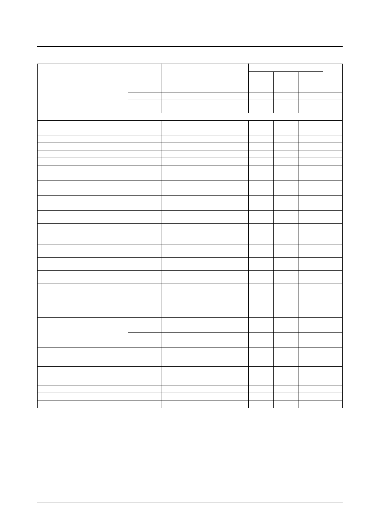
Electrical Characteristics at Ta = 25°C, VCC1 = 12 V, VCC2 = 5 V
Note: Items marked with an asterisk are design target values and are not tested.

No. 5653-3/7
LB1916
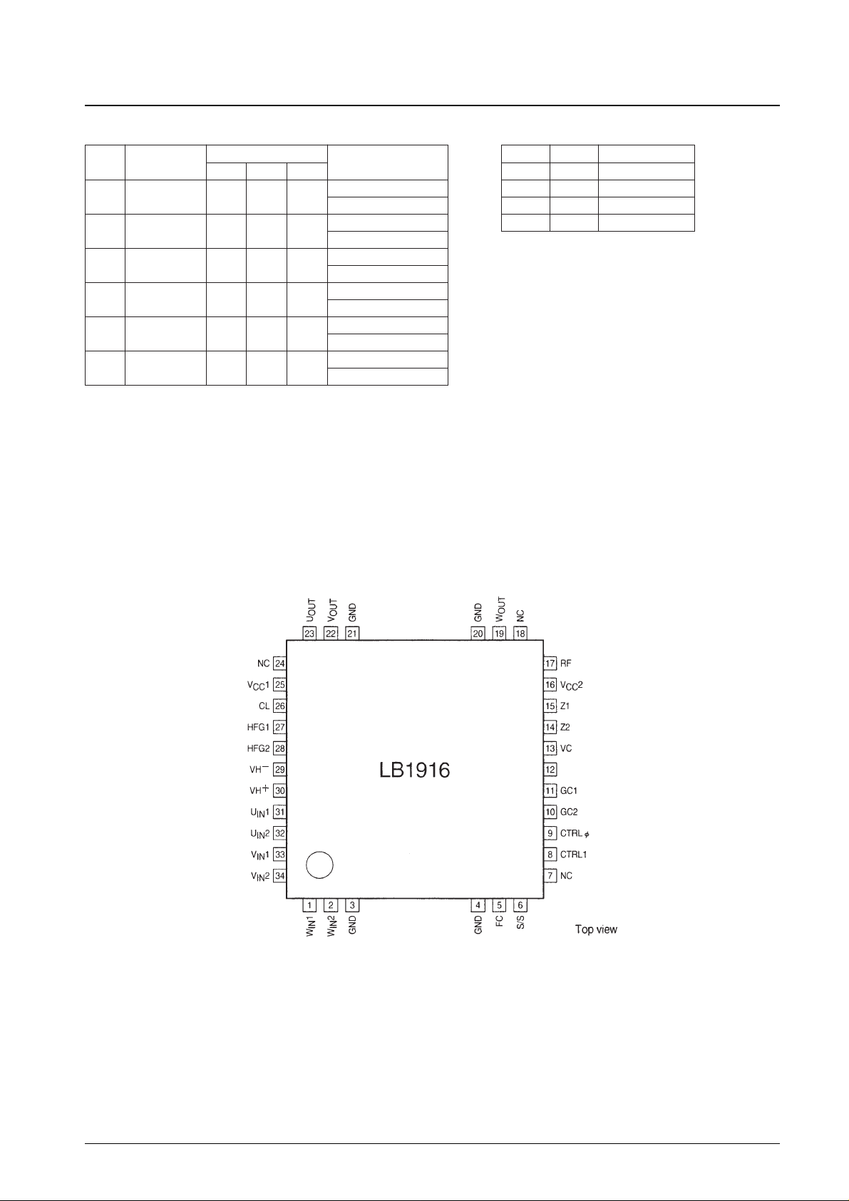
Hall Logic Truth Table
An input “H” state is defined as UIN1 > UIN2, VIN1 > VIN2, and the potential
difference is at least 0.2 V.
When VC> V
CREF
: Forward rotation
When V
C
< V
CREF
: Reverse rotation
Source → Sink
Hall input
Forward/reverse control
U
IN
V
IN
W
IN
1
W → V
H H L
Forward
V → W Reverse
2
W → U
H L L
Forward
U → W Reverse
3
V → W
L L H
Forward
W → V Reverse
4
U → V
L H L
Forward
V→> U Reverse
5
V → U
H L H
Forward
U → V Reverse
6
U → W
L H H
Forward
W → U Reverse
Mode Switching Truth Table
The low level is 0 to 1.0 V
The high level is 4.0 V or higher
CTRL0 CTRL1 Mode
L L Control
L H Control
H L Acceleration
H H Deceleration
Pin Assignment
V
CREF
 Loading...