

SANYO LB1896 Datasheet
Ordering number: EN5225
Monolithic Digital IC
LB1896
3-phase Brushless Motor Driver for
CD-ROM Spindle Drive Use
Overview
The LB1896 is a 3-phase brushless motor driver IC that is
ideal for driving CD-ROM spindle motors.
Functions and Features
v 120°voltage linear technique
v V-type control voltage
v Switchable control gain
v Control, noncontrol, acceleration/deceleration mode select
pins built in.
v Start/Stop pin built in, Hall bias built in.
Specifications
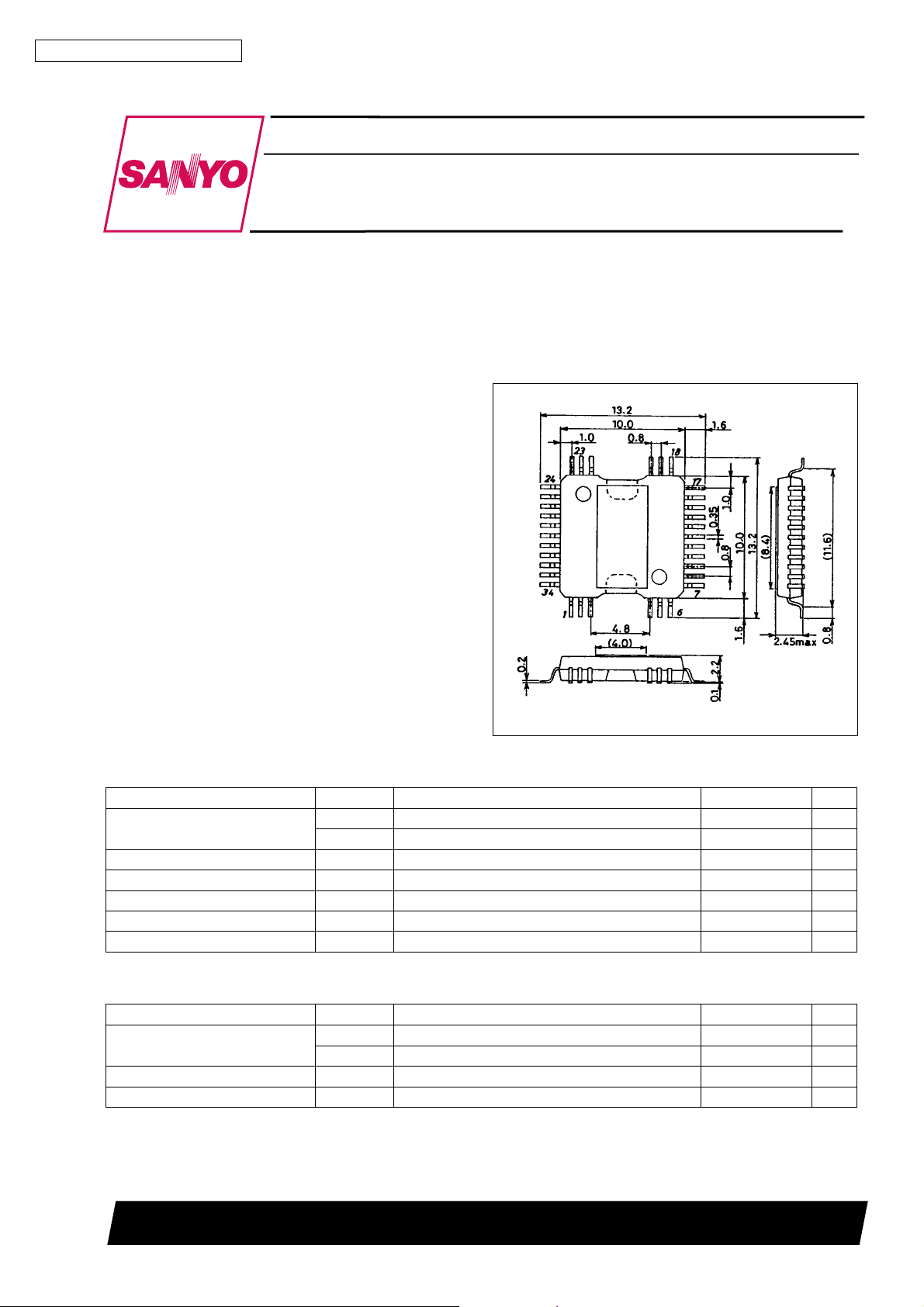
Package Dimensions
unit : mm
3219-QFP34H-C
[LB1896]
SANYO : QFP34H – C
Absolute Maximum Ratings atTa=25°C
Parameter Symbol Conditions Ratings Unit
V
1 max 20 V
Maximum supply voltage
Applied output voltage V
Output current I
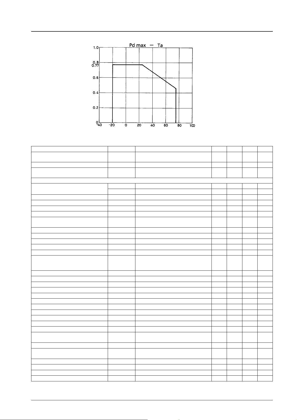
Allowable power dissipation Pd max Independent IC 0.77 W
Operating temperature Topr –20 to +75
Storage temperature Tstg –55 to +150
CC
V
2 max 7.0 V
CC
OU, V, W
OUT
1.2 A
20 V
Operating Conditions atTa=25°C
Parameter Symbol Conditions Ratings Unit
V
1 5 to 18 V
Supply voltage
V
input voltage V
Cref
V
input voltage V
NS
CC
V
2VCC1 ^ VCC2 4.3 to 6.5 V
CC
Cref
NS
VCC2/2 ±1.0 V
0toVCC2 –1.0 V
C
°
C
°
SANYO Electric Co.,Ltd. Semiconductor Bussiness Headquarters
TOKYO OFFICE Tokyo Bldg., 1-10, 1 Chome, Ueno, Taito-ku, TOKYO, 110 JAPAN
13096HA(II) No.5225-1/8
LB1896
Allowable power dissipation, Pd max — W
Ambient temperature, Ta — °C
Electrical Characteristics atTa=25°C, VCC1=12V,VCC2=5V
Parameter Symbol Conditions min typ max Unit
V
= open, V
Supply current 1 I
Supply current 2 I
Supply current 3 I
1
CC
2V
CC
3
CC
C
V
=5V
S/S
= open, V
C
= open, V
V
C
V
=0V,(ICCof VCC1)
S/S
[Drive block]
Output saturation voltage
V
V
Output TRS sustaining voltage V
Output static voltage V
Hall amplifier input offset voltage V
Hall amplifier input bias current I
Hall amplifier common-mode input
voltage range
Hall input/output voltage gain G
Control/output drive gain 1 G
Control/output channel difference 1 ∆G
Control/output drive gain 2 G
Control/output channel difference 2 ∆G
1I
O(sat)
2I
O(sat)
O(sus)
OQ
H offset
H bias
V
Hch
VHO
1 RZ1 = RZ2, GC1 = L, GC2 = L 26 29 dB
VCO
1 RZ1 = RZ2, GC1 = L, GC2 = L –1.5 +1.5 dB
VCO
2 RZ1 = RZ2, GC1 = L, GC2 = H 32 35 dB
VCO
2 RZ1 = RZ2, GC1 = L, GC2 = H –1.9 +1.9 dB
VCO
= 0.4 A, sink + source 1.6 2.2 V
OUT
= 0.8 A, sink + source 2.0 3.0 V
OUT
I
=20mA 20 V
OUT
VC= 2.5 V, V
RZ1 = RZ2, GC1 = L, GC2 = L
Input dead zone voltage V
Input bias current 1 I
B SERVOVC
Input bias current 2 I
S/S pin high voltage V
S/S pin low voltage V
Gain control 1 high voltage V
Gain control 1 low voltage V
Gain control 2 high voltage V
Gain control 2 low voltage V
S/S pin input current I
Gain control 1, 2 current I
Rotation output saturation voltage V
Rotation output saturation sustaining
voltage
(sat) H.FGIO
V
(sus) H.FG
Hall bias voltage V
CTRL pin high voltage V
CTRL pin low voltage V
CTRL input current I
DZ
B n.s
S/S H
S/S L
GC1 H
GC1 L
GC2 H
GC2 L
S/S
GC
H
CTRL H
CTRL L
CTRL
V
(voltage between out and out) =
O
0.1 V
= 1.0 V 500 nA
VNS= 1.0 V 500 nA
Input is CMOS level 4 V
Note) S/S pin Vth = VCC2/2 1 V
Input is at CMOS level. 4 V
Note) GC1 pin Vth = 2.0 V 1 V
Input is at CMOS level. 4 V
Note) GC2 pin Vth = 2.0 V 1 V
Input voltage=5V 50 100 µA
Input voltage=5V 53 110 µA
= –5 mA 0.24 0.5 V
± IO= 5 mA, RH= 200 Ω 0.7 0.97 1.2 V
Common for CTRL1 and CTRL2
input CMOS level
Note) CTRL pin Vth = 2.5 V 1.0 V
Input voltage=5V 53 110 µA
TSD operation voltage TSD Design target 150 180 210 °C
TSD hysteresis ∆TSD Design target 15 °C
= open, RL= ∞,
Cref
= open 7.5 10.5 mA
Cref
= open, RL= ∞,
Cref
= 2.5 V 5.7 6.0 6.3 V
Cref
17 30 mA
0.9 3 mA
–5 +5 mV
15µA
1.3 2.2 V
40 43 46 dB
±13 ±38 ±55 mV
4V
7V
Note) Vth is a design target and not measured.
No.5225-2/8
Mode Switching Truth Table
CTRL0 CTRL1 Mode
L L Control
L H Noncontrol
H L Acceleration
H H Deceleration
L = 0 to 1.0 V
H = 4.0 V or more
Hall Logic Truth Table
LB1896
Source → Sink
1
2
3
4
5
6
W → V
V → W
W → U
U → W
V → W
W → V
U → V
V → U
V → U
U → V
U → W
W → U
U
IN
HHL
HLL
LLH
LHL
HLH
LHH
Hall input
V
IN
W
IN
An input is considered to be HIGH when UIN1 > UIN2, VIN1 > VIN2, and WIN1 > WIN2 by 0.2 V or more.
Forward when V
Reverse when VC< V
> V
C
Cref
Cref
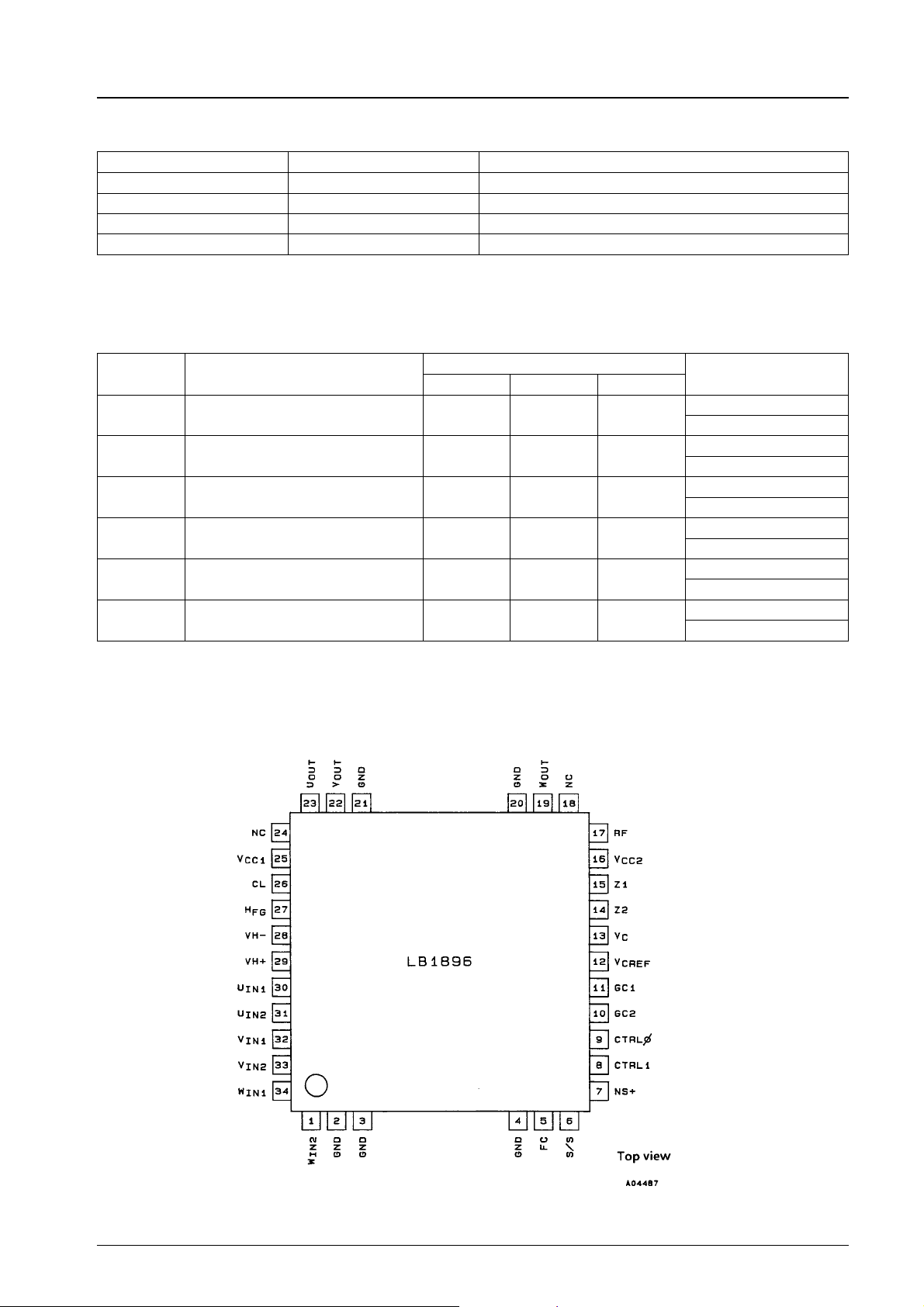
Pin Assignment
F/R Control
Forward
Reverse
Forward
Reverse
Forward
Reverse
Forward
Reverse
Forward
Reverse
Forward
Reverse
No.5225-3/8
 Loading...