

SANYO LB1895D, LB1895 Datasheet

Ordering number: EN5634
Monolithic Digital IC
LB1895, 1895D
3-Phase Brushless Motor Driver for
CD-ROM Spindle Motors
Overview
The LB1895 and LB1895D are 3-phase brushless motor drivers
for use in CD-ROM spindle motors.
Functions and Features
.
Current linear drive
.
V-type control amplifier built in
.
Because the power supply for the bias circuit on the upper
output side is separate, output with low saturation can be
attained by boosting only that power supply. (Effective when
V
=5V)
CC
.
Because current is detected on the upper side, there is no
voltage loss due to the RF resistance. In addition, the RF
voltage reduces the power dissipation within the IC.
(Effective when V
.
Start/Stop function built in
.
Thermal shutdown circuit built in
.
Overcurrent protection circuit built in
.
Two-channel Hall signal comparator built in.
(For detecting rotation direction and Hall FG output)
.
Hall device bias built in
CC
=5V)
Package Dimensions
unit : mm
3222-HSOP28
[LB1895]
114
0.8
unit : mm
3196-DIP30SD
2.7
15.2
0.3
0.8
[LB1895D]
1528
5.6
0.2
1.8max
0.1
SANYO : HSOP28
1.0
7.6
0.5
SANYO : DIP30SD
SANYO Electric Co.,Ltd. Semiconductor Bussiness Headquarters
TOKYO OFFICE Tokyo Bldg., 1-10, 1 Chome, Ueno, Taito-ku, TOKYO, 110 JAPAN
4097HA(II) No.5634-1/12

LB1895, 1895D
Specifications
Maximum Ratings atTa=25°C
Parameter Symbol Conditions Ratings Unit
Maximum supply voltage 1 V
Maximum supply voltage 2 V
Maximum supply voltage 3 V
Applied output voltage V
Applied input voltage V
Output current I
Allowable power dissipation Pd max
Operating temperature Topr –20 to +75
Storage temperature Tstg –55 to +150
Operating Conditions atTa=25°C
Parameter Symbol Conditions Ratings Unit
Supply voltage
1 max 7 V
CC
2 max 14.4 V
CC
3 max 14.4 V
CC
max 14.4 V
O
max VCC1V
I
max 1.0 A
O
Indepent IC [LB1895] 0.5 W
Glass epoxy board
(114.3 × 762 × 1.5 mm) [LB1895D]
14to6V
V
CC
V
2 ^ VCC1 4 to 13.6 V
CC
V
3 2 to 13.6 V
CC
2.4 W
C
°
C
°
Application Examples atTa=25°C
(1) 12 V model
Power supply pins Conditions Ratings Unit
V
1 REG. voltage 4 to 6 V
CC
V
2=VCC3 UN-REG. voltage 4to 13.6 V
CC
(2) 5 V model
Power supply pins Conditions Ratings Unit
V
1=VCC3 REG. voltage 4 to 6 V
CC
V
2 Boost voltage or REG. voltage (Note) 4 to 13.6 V
CC
Note: If VCC2 is used as the boost voltage, output with low saturation can be used.
No.5634-2/12
LB1895, 1895D
Electrical Characteristics atTa=25°C, VCC1=5V,VCC2=VCC3=12V
(Unless otherwise specified)
Parameter Symbol Conditions min typ max Unit
[Supply current]
Supply current 1 I
Supply current 2 I
Supply current 3 I
Output quiescent current 1 I
Output quiescent current 2 I
Output quiescent current 3 I
[Output]
Upper saturation voltage 1 V
Lower saturation voltage 1 V
Upper saturation voltage 2 V
Lower saturation voltage 2 V
Current limiter setting voltage VC
[Hall Amplifier]
Hall amplifier common-mode
input voltage range
Hall amplifier input bias current IH
Minimum Hall input level VH
[S/S pin]
High-level voltage V
Low-level voltage V
Input current I
LEAK current I
[Control stage]
VC pin input current I
VC
pin input current I
REF
Voltage gain VG
Rising threshold voltage VC
Rising threshold voltage width ∆ VC
[Hall supply]
Hall supply voltage V
Allowable current I
[Thermal shutdown]
Operating temperature T
Hysteresis ∆T
[Hall comparator]
Input offset voltage V
Input hysteresis V
Output ON voltage V
Output OFF voltage V
Output current (sink) I
Note: When in S/S OFF (standby) state, the Hall comparator goes high.
*D stands for design target; this value is not measured.
1 VC=VC
CC
2 VC=VC
CC
3 VC=VC
CC
CC1OQ
CC2OQ
CC3OQ
OU
OD
OU
OD
VH
COM
S/SH
S/SL
S/SI
S/SL
VC
VCREF
H
TSD
TSD
offset 10 mV
HCI
HCI
OU
OD
SINK
V
V
V
1
IO= –0.5 A, VCC1=5V,VCC2=VCC3 = 12 V 0.8 1.3 V
1I
O
2I
O
2I
O
RRF = 0.43 Ω 0.25 0.32 0.4 V
L
IB
IN
V
V
VC=VC
VC=VC
∆VRF/∆VC 0.2 0.25 0.3 Times
CO
VC
TH
VC
TH
IH= 5 mA 1.0 1.6 V
H
*D 150 180 210
*D15
hys 3 8 15 mV
Note 4.7 V
REF
REF
REF
= 0 V 200 µA
S/S
= 0 V 30 µA
S/S
= 0 V 30 µA
S/S
= 0.5 A, VCC1=5V,VCC2=VCC3 = 12 V 0.3 0.5 V
= –0.5 A, VCC1=VCC3=5V,VCC2 = 12 V 0.3 0.5 V
= 0.5 A, VCC1=VCC3=5V,VCC2 = 12 V 0.3 0.5 V
= 5 V 200 µA
S/S
= 0 V –30 µA
S/S
= 2.5 V 1 3 µA
REF
= 2.5 V 1 3 µA
REF
= 2.5 V 2.35 2.65 V
REF
= 2.5 V 50 150 mV
REF
47mA
0 0.5 mA
150 250 µA
1
V
1.2
CC
–1.0
V
12µA
60 mVp-p
2.0 VCC1V
0.7 V
20 mA
C
°
C
°
0.3 V
3mA
No.5634-3/12
LB1895, 1895D
Truth Table
1
2
3
4
5
6
W phase → V phase
V phase → W phase L
W phase → U phase
U phase → W phase L
V phase → W phase
W phase → V phase L
U phase → V phase
V phase → U phase L
V phase → U phase
U phase → V phase L
U phase → W phase
W phase → U phase L
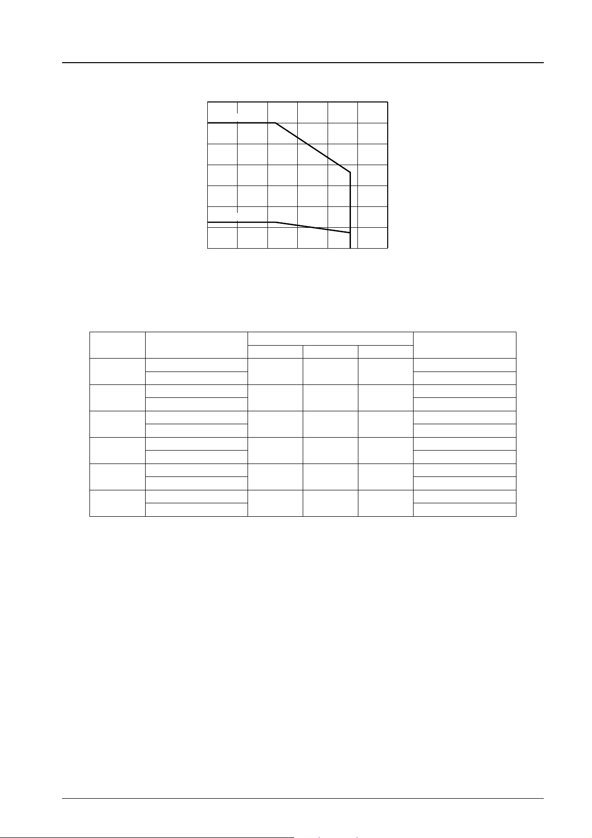
2.8
2.4
2.0
1.6
1.2
0.8
0.4
0
|
20 20 400 60 80 100
Allowable power dissipation, Pd max – W
Source → sink
Pd max – Ta
LB1895D
LB1895
Ambient temperature, Ta –°C
Input
UVW
HHL
HLL
LLH
LHL
HLH
LHH
Control
VC
H
H
H
H
H
H
Inputs
H: For each phase input 2, phase input 1 is at a higher electric potential of 0.2 V or more.
L: For each phase input 2, phase input 1 is at a lower electric potential of 0.2 V or more.
No.5634-4/12
 Loading...