

Page 1
Ordering number : EN4626
73098HA (OT)/91494TH (OT) B8-0603 No. 4626-1/9
Overview
The LB1882V is a three-phase brushless motor driver IC
that is particularly well-suited for driving spindle motors
in portable AV equipment such as DAT, CD and MD
products.
Features
• Current linear drive: allows external capacitances to be
minimized.
• Motor voltage control: reduces power dissipation.
• Support for motor drive at power supply voltages as low
as 1.8 V
• Built-in torque ripple correction circuit
• Built-in saturation prevention circuit
• Built-in AGC circuit
• Built-in thermal shutdown circuit
• Built-in current limiter
• Built-in FG amplifier
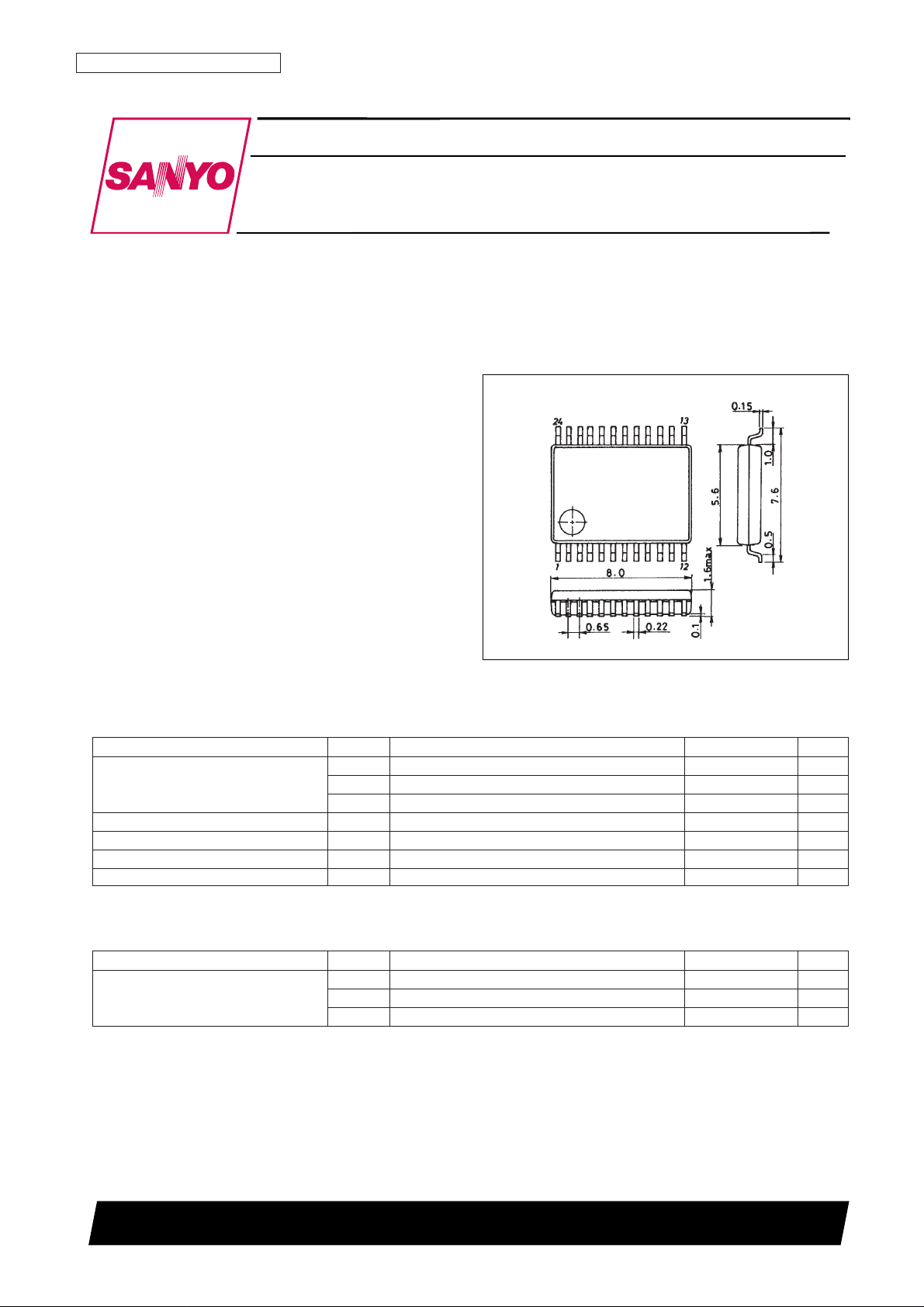
Package Dimensions
unit: mm
3175A-SSOP24
SANYO: SSOP24
[LB1882V]
LB1882V
SANYO Electric Co.,Ltd. Semiconductor Bussiness Headquarters
TOKYO OFFICE Tokyo Bldg., 1-10, 1 Chome, Ueno, Taito-ku, TOKYO, 110-8534 JAPAN
Three-Phase Brushless Motor Driver
Monolithic Digital IC
Specifications
Absolute Maximum Ratings at Ta = 25°C
Parameter Symbol Conditions Ratings Unit
V
CC
1 max 8V
Maximum supply voltage V
CC
2 max 12 V
V
S
max VCC1V
Maximum output current I
O
max 1.0 A
Allowable power dissipation Pd max 0.5 W
Operating temperature Topr –20 to +75 °C
Storage temperature Tstg –55 to +150 °C
Operating Conditions at Ta = 25°C
Parameter Symbol Conditions Ratings Unit
V
CC
1 1.8 to 6.0 V
Supply voltage V
CC
2 3 to 10 V
V
S
Up to VCC1V
Page 2
Electrical Characteristics at Ta = 25°C, VCC1 = 2.5 V, VCC2 = 4.5 V, VS= 1 V
Note: * Items marked with an asterisk are design target values and are not tested.
No. 4626-2/9
LB1882V
Parameter Symbol Conditions min typ max Unit Note
I
CC
1 5 8 mA
Current drain I
CC
2 2 mA
I
S
IS– I
L
1 mA
I
CC 1OQVSTBY
= 0 V 10 µA
Output quiescent current I
CC 2OQVSTBY
= 0 V 10 µA
I
SOQ
V
STBY
= 0 V 10 µA
Output saturation voltage
V
OU (sat)
1 VRF= 40 mV, RL= 100 Ω (Y) 25 65 mV
upper side
V
OU (sat)
2 VRF= 100 mV, RL= 100 Ω (Y) 25 65 mV
Output residual voltage
V
OD (sat)
1 VRF= 40 mV, RL= 100 Ω (Y) 200 280 mV
lower side
V
OD (sat)
2 VRF= 100 mV, RL= 100 Ω (Y) 285 365 mV
Hall amplifier input offset voltage V
Hoffset
–5 +5 mV *
Hall amplifier common-mode
V
HCOM
1.2 2.5 V
input voltage range
Standby pin high level voltage V
STBYH
2.0 V
Standby pin low level voltage V
STBYL
0.4 V
Standby pin input current I
LSTBYVSTBY
= 4.5 V 120 µA
Standby pin leakage current I
LSTBYVSTBY
= 0 V –30 µA
FRC pin high level voltage V
FRCH
1.6 V
FRC pin low level voltage V
FRCL
0.4 V
FRC pin input current I
IFRC
V
FRC
= 4.5 V 100 µA
FRC pin leakage current I
LFRC
V
FRC
= 0 V –30 µA
Thermal shutdown operating
T
TSD
150 180 210 °C *
temperature
Thermal shutdown hysteresis ∆T
TSD
15 °C *
[FG Amplifier]
Common-mode input
V
ICR
1.2 3.3 V
voltage range
Input offset voltage V
IO
–5 +5 mV *
Output saturation voltage V
SINKRL
= 10 kΩ 0.2 V
Output current (sink) I
SINK
2 mV
Page 3
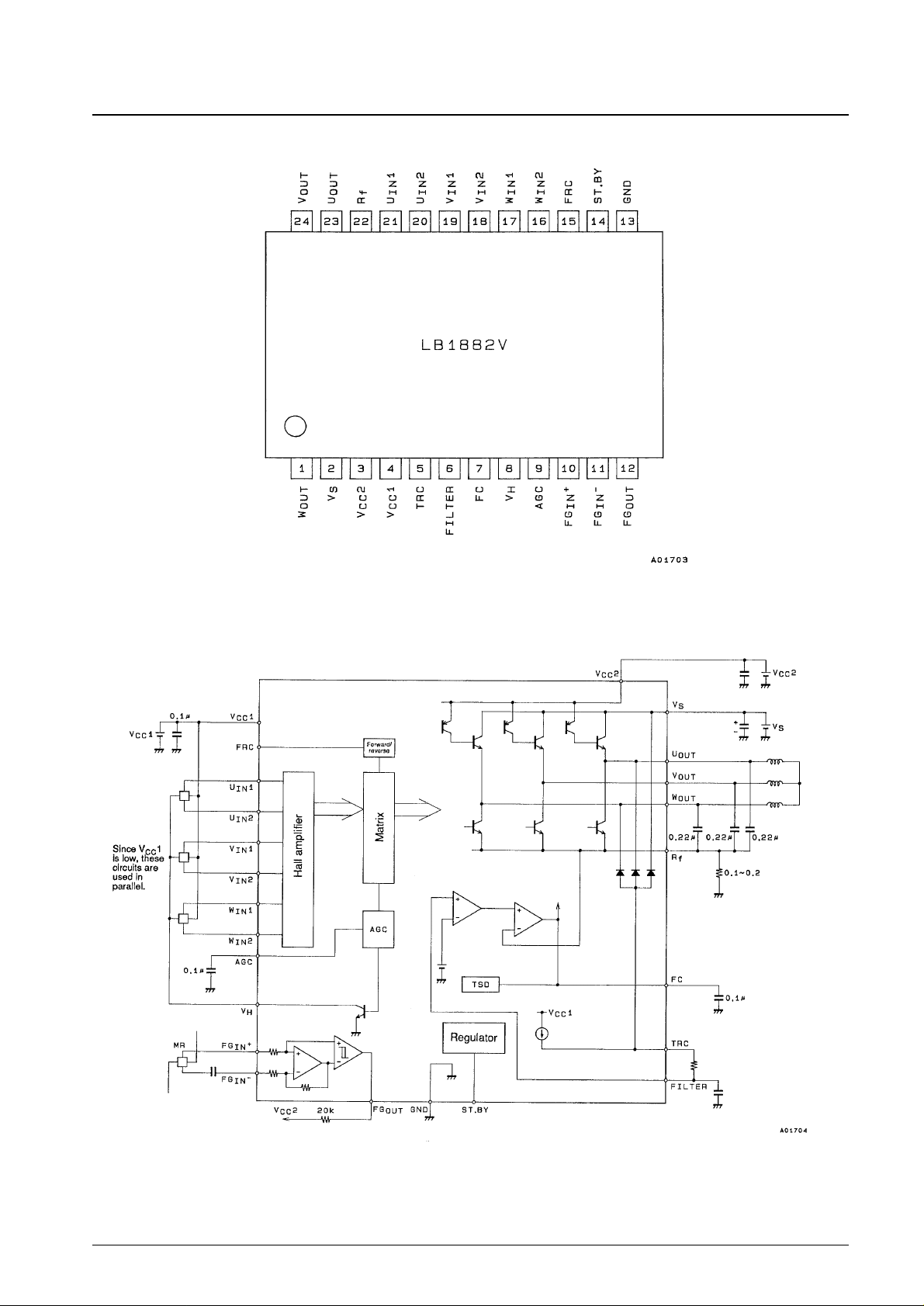
Pin Assignment
Block Diagram and Sample Application Circuit
No. 4626-3/9
LB1882V
Top view
Unit (resistance: Ω, capacitance: F)
Page 4

Truth Table
Inputs: “H” means that the input 1 potential for the corresponding phase is at least 0.2 V higher than the input 2 potential.
“L” means that the input 1 potential for the corresponding phase is at least 0.2 V lower than the input 2 potential.
Forward/reverse control: “H”: 1.6 V to V
CC
2
“L”: 0 V to 0.4 V
Pin Functions
No. 4626-4/9
LB1882V
Source Input
Forward/reverse
Sink U V W
control
1
W phase
→ V phase
H H L
L
V phase → W phase H
2
W phase → U phase
H L L
L
U phase → W phase H
3
V phase → W phase
L L H
L
W phase → V phase H
4
U phase → V phase
L H L
L
V phase → U phase H
5
V phase → U phase
H L H
L
U phase → V phase H
6
U phase → W phase
L H H
L
W phase → U phase H
Continued on next page.
Pin No. Symbol Pin voltage Equivalent circuit Pin function
2
3
4
5
6
V
S
VCC2
V
CC
1
TRC
FILTER
≤ V
CC
1
≥ V
CC
1
3 V to 10 V
1.8 V to 6 V
Power supply that provides the motor voltage and
determines the output amplitude
This voltage must be lower than V
CC
1.
Power supply that provides the voltage for the
source side pre-drive PNP transistor and the FG
amplifier
Power supply that provides all voltages other than
the motor voltage, the source side pre-drive voltage
and the FG amplifier voltage
Coil output waveform lower side saturation
waveform detection
The coil output saturation prevention function
operates using an RC filter (a resistor between this
pin and the TRC pin and a capacitor between this
pin and ground) connected at this pin. Motor speed
(r.p.m.) control can then be achieved by adjusting
the voltage on pin V
S
. The torque ripple correction
amount can be adjusted by adjusting this RC
constant.
Unit (resistance: Ω)
Page 5

Continued from preceding page.
No. 4626-5/9
LB1882V
Pin No. Symbol Pin voltage Equivalent circuit Pin function
7
8
9
10
11
12
FC
V
H
AGC
FG
IN
+
FG
IN
–
FG
OUT
1.2 V min
3.3 V max
V
CC
2 max
Frequency characteristics correction
The capacitor connected between this pin and
ground stops closed-loop oscillation in the current
control system.
The Hall elements are connected between this pin
and V
CC
1. The AGC circuit adjusts the Hall bias
current so that the coil output slope remains fixed.
Since the Hall amplifier common-mode voltage
range is reduced when a low voltage is used for
V
CC
1, the Hall elements should be connected in
parallel.
A capacitor is inserted between this pin and
ground. The AGC circuit controls the Hall bias
current so that the coil output slope remains fixed.
FG amplifier input
FG amplifier output
Continued on next page.
Unit (resistance: Ω)
Page 6

Continued from preceding page.
No. 4626-6/9
LB1882V
Pin No. Symbol Pin voltage Equivalent circuit Pin function
13
14
15
16
17
18
19
20
21
22
23
24
1
GND
ST, BY
FRC
W
IN
2
W
IN
1
V
IN
2
V
IN
1
U
IN
2
U
IN
1
RF
U
OUT
V
OUT
W
OUT
VCC2 max
V
CC
2 max
1.2 V min
2.5 V max
(V
CC
1 is 2.5 V
when Ta is 25°C.)
Ground for all circuits other than the output circuits
All circuits stop when this pin falls below 0.4 V or is
open. In this state, the circuit current will be 10 µA
or lower. Set this pin to 2 V or higher to operate the
LB1882V in the motor drive state.
Motor forward/reverse switching
Low level: Forward (0 to 0.4 V)
High level: Reverse (1.6 V to V
CC
2)
W-phase Hall device input
The logic high level is the state
where W
IN
1 > WIN2.
V-phase Hall device input
The logic high level is the state
where V
IN
1 > VIN2.
U-phase Hall device input
The logic high level is the state
where U
IN
1 > UIN1.
Output transistor ground
Detecting the voltage on this pin is used to
implement fixed current drive and the current limiter
function.
U-phase output
V-phase output
W-phase output
Unit (resistance: Ω)
Page 7

LB1882V Operating Principles
The LB1882V implements a current linear drive method, and controls the motor speed with the motor power supply
voltage by always preventing coil output saturation and holding the output saturation voltage fixed.
1. Control system (See page 8)
• The TRC pin outputs a signal consisting of the coil output voltage lower-side envelope plus the diode rising
voltage.
• The TRC waveform, after the high-frequency components are reduced by a low-pass filter consisting of an RC
circuit connected to the FILTER pin, is input to the FILTER pin. The cutoff frequency is 1/2π·RC.
• The FILTER pin voltage is input to the control amplifier plus side. The control amplifier minus side is connected
to the reference voltage and the control amplifier operates to hold the FILTER pin at the same potential as this
reference voltage. As long as this reference voltage exceeds the output transistor saturation voltage, the coil output
will operate in the unsaturated state.
• The output current (the RF current) operates as a fixed current drive, since lower-side the RF voltage, is held at a
fixed level by the second stage of the control amplifier.
Note: The low-frequency components that are not removed by the TRC pin RC filter function as motor torque ripple
correction signals.
2. Drive system (See page 8.)
• The Hall element output is wave shaped by the first stage of the Hall amplifier.
• The Hall amplifier output waveform is synthesized by the matrix amplifier, which creates a waveform phase
delayed by 30°.
• This waveform is voltage-to-current converted and is then further current amplified and output as the coil current
by the power amplifier. Since the upper and lower transistor drive ratios differ here (the upper transistor drive ratio
is larger), the upper side voltage waveform is saturated, and the lower-side voltage waveform is unsaturated.
Note: The AGC circuit controls the Hall bias current so that the matrix amplifier output waveform has a fixed
amplitude.
No. 4626-7/9
LB1882V
Page 8

Control System Signal Flow
No. 4626-8/9
LB1882V
Page 9

PS No. 4626-9/9
LB1882V
This catalog provides information as of July, 1998. Specifications and information herein are subject to change
without notice.
■ No products described or contained herein are intended for use in surgical implants, life-support systems, aerospace
equipment, nuclear power control systems, vehicles, disaster/crime-prevention equipment and the like, the failure of
which may directly or indirectly cause injury, death or property loss.
■ Anyone purchasing any products described or contained herein for an above-mentioned use shall:
➀ Accept full responsibility and indemnify and defend SANYO ELECTRIC CO., LTD., its affiliates, subsidiaries and
distributors and all their officers and employees, jointly and severally, against any and all claims and litigation and all
damages, cost and expenses associated with such use:
➁ Not impose any responsibility for any fault or negligence which may be cited in any such claim or litigation on
SANYO ELECTRIC CO., LTD., its affiliates, subsidiaries and distributors or any of their officers and employees
jointly or severally.
■ Information (including circuit diagrams and circuit parameters) herein is for example only; it is not guaranteed for
volume production. SANYO believes information herein is accurate and reliable, but no guarantees are made or implied
regarding its use or any infringements of intellectual property rights or other rights of third parties.
 Loading...