

Page 1
Any and all SANYO products described or contained herein do not have specifications that can handle
applications that require extremely high levels of reliability, such as life-support systems, aircraft’s
control systems, or other applications whose failure can be reasonably expected to result in serious
physical and/or material damage. Consult with your SANYO representative nearest you before using
any SANYO products described or contained herein in such applications.
SANYO assumes no responsibility for equipment failures that result from using products at values that
exceed, even momentarily, rated values (such as maximum ratings, operating condition ranges, or other
parameters) listed in products specifications of any and all SANYO products described or contained
herein.
Monolithic Digital IC
Ordering number : ENN4456A
73099TH (OT)/43098HA (OT)/12194TS A8-9620 No. 4456-1/7
SANYO Electric Co.,Ltd. Semiconductor Company
TOKYO OFFICE Tokyo Bldg., 1-10, 1 Chome, Ueno, Taito-ku, TOKYO, 110-8534 JAPAN
Three-Phase Brushless Motor Driver IC
LB1881V
Overview
The LB1881V is a three-phase brushless motor driver IC
designed for use as a camcorder capstan or drum motor
driver, or as a digital audio tape player/recorder motor
driver.
Features
• 120° voltage linear system
• Appropriate for portable applications, since the
LB1881V reduces system power requirements by using
motor voltage control for speed control.
• Built-in torque ripple compensation circuit
• Small external capacitances due to the adoption of a soft
switching technique (chip capacitor).
• Built-in thermal shutdown circuit
• Built-in FG amplifier
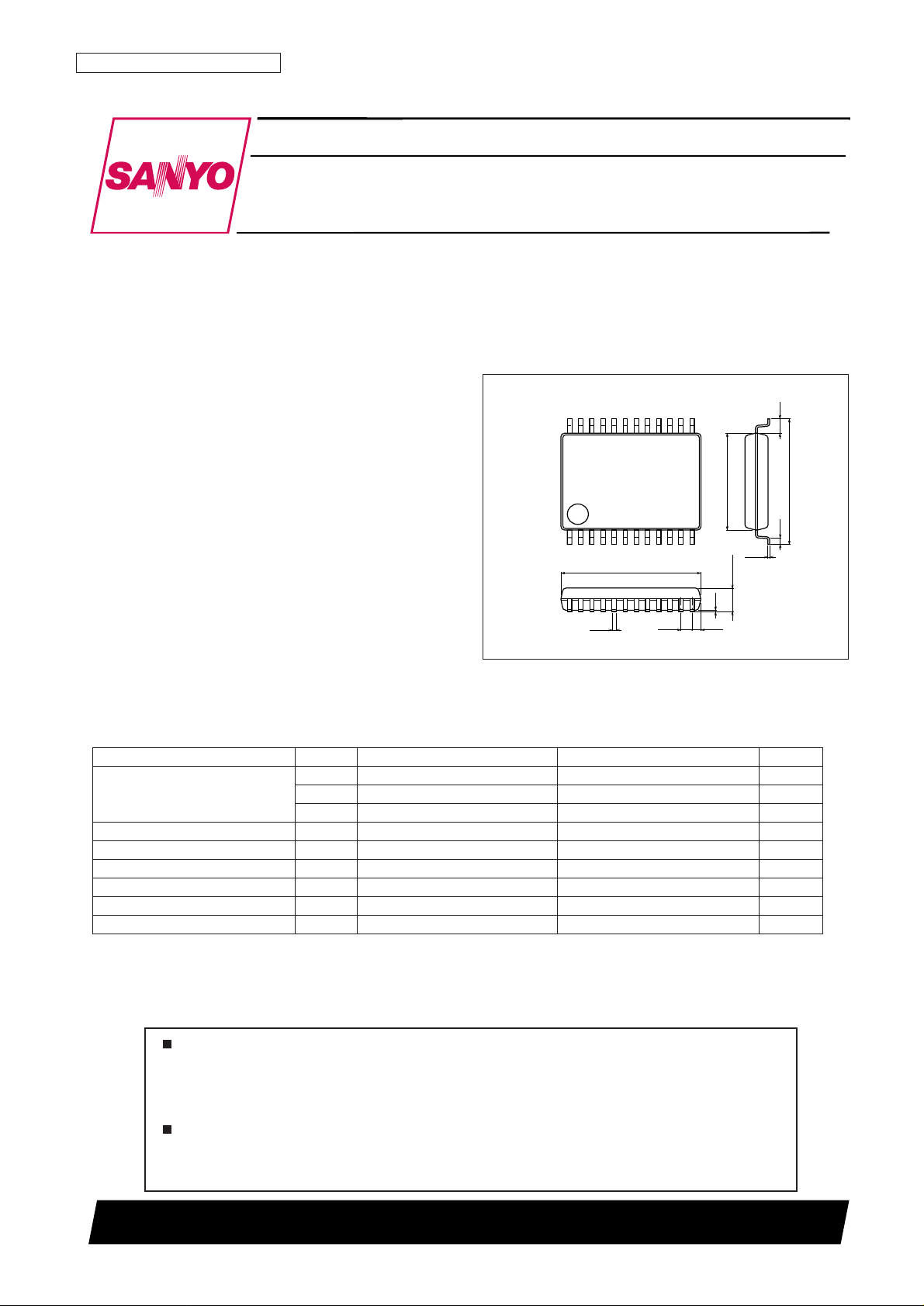
Package Dimensions
unit: mm
3175A-SSOP24
112
13
7.6
8.0
0.5
5.6
0.1
1.6max
1.0
24
0.65
0.22
0.43
0.15
SANYO: SSOP24
[LB1881V]
Specifications
Absolute Maximum Ratings at Ta = 25°C
Parameter Symbol Conditions Ratings Unit
V
CC
1 max 7 V
Supply voltage V
CC
2 max 12 V
V
S
max VCC2V
Output applied voltage V
O
max VS+ 2 V
Input applied voltage V
I
max All input pins VCC1V
Output current I
O
max 1.0 A
Allowable power dissipation Pd max 0.5 W
Operating temperature Topr –20 to +75 °C
Storage temperature Tstg –55 to +150 °C
Page 2
No. 4456-2/7
LB1881V
Electrical Characteristics at Ta = 25°C, VCC1 = 5 V, VCC2 = 7 V, VS= 3 V
Ratings
Parameter Symbol Conditions
min typ max
Unit
I
CC
1 VBR= 5 V 3.0 5.0 mA
Supply current I
CC
2 VBR= 5 V 6.5 10.0 mA
I
S
VBR= 5 V, RL= ∞ 5.0 mA
Output quiescent current
I
CCOQ
V
STBY
= 0 V 100 µA
I
SOQ
V
STBY
= 0 V, RL= ∞ 150 µA
Output saturation voltage V
O(sat)
I
OUT
= 0.6 A, sink + source 1.7 V
Output TRS withstand voltage V
O(sus)
I
OUT
= 20 mA*1 12 V
Output quiescent voltage V
OQ
VBR= 5 V 1.45 1.55 1.65 V
Hall amplifier input offset voltage V
HOFFSET
*1 –5 +5 mV
Hall amplifier common mode input
V
HCOM
1.4 2.8 V
voltage range
Hall I/O voltage gain GV
HO
Rangle = 8.2 kΩ 34.0 37.0 40.0 dB
Brake pin high level voltage V
BRH
2.0 V
Brake pin low level voltage V
BRL
0.8 V
Brake pin input current I
BRIN
120 µA
Brake pin leakage current I
BRLEAK
–30 µA
FRC pin high level voltage V
FRCH
2.8 V
FRC pin low level voltage V
FRCL
1.2 V
FRC pin input current I
FRCIN
100 µA
FRC pin leakage current I
FRCLEAK
–30 µA
Upper side residual voltage V
XH
I
OUT
= 100 mA, VCC2 = 6 V, VS= 2 V 0.285 0.455 V
Lower side residual voltage V
XL
I
OUT
= 100 mA, VCC2 = 6 V, VS= 2 V 0.350 0.440 V
Residual voltage inflection point V
S∆VX
I
OUT
= 100 mA, VCC2 = 6 V*1 0.9 V
Overlap level OL V
CC
2 = 6 V, VS= 3 V, RL= 100 Ω (Y) 60 70 80 %
Overlap vertical difference ∆OL V
CC
2 = 6 V, VS= 3 V, RL= 100 Ω (Y) –10 0 +10 %
Standby on voltage V
STBYL
*2 –0.2 +0.8 V
Standby off voltage V
STBYH
2 5 V
Standby pin bias current I
STBYIN
100 µA
Thermal protection circuit operating
T
TSD
*1 150 180 210 °C
temperature
Thermal protection circuit hysteresis ∆T
TSD
*1 15 °C
FG amplifier input offset voltage V
FG OFFSET
–8 +8 mV
Open loop voltage gain GV
FG
f = 10 kHz 43 dB
Source output saturation voltage V
FG OU
IO= –2 mA 3.7 V
Sink output saturation voltage V
FG OD
IO= 2 mA 1.3 V
Common mode signal exclusion ratio G
HR
*1 80 dB
FG amplifier common mode input
V
FG CH
0 3.5 V
voltage range
Phase margin φM *1 20 deg
Schmitt amplifier threshold voltage V
FGS SH
V
FGIN
+
= 2.5 V,
2.45 2.50 2.55 V
when V
FGOUT
2 goes from high to low
Schmitt amplifier hysteresis width V
FGS HIS
V
FGIN
+
= 2.5 V 20 40 60 mV
Note: 1. These are target settings, and are not measured. The overlap ratings are taken as test ratings without change.
2. When the standby pin is open the IC will be in the standby state.
Allowable Operating Ranges at Ta = 25°C
Parameter Symbol Conditions Ratings Unit
V
CC
1 VCC1 ≤ VCC2 4.0 to 6.0 V
Supply voltage V
CC
2 4 to 10 V
V
S
Up to VCC2 V
Page 3
No. 4456-3/7
LB1881V
Pin Assignment
Block Diagram
Top view
Allowable power dissipation, Pd max – W
Ambient temperature, Ta – °C
Page 4

No. 4456-4/7
LB1881V
Pin Functions
Pin No. Symbol Pin voltage Equivalent circuit Pin function
3 V
S
≤ VCC2 Power supply input that determines the output
amplitude. It must be set to a voltage equal or
lower than V
CC
2.
4 V
CC
2 4 to 10 V Power supply for power amplifier systems other
than motor drive transistors. Power supply pin
that provides voltage for blocks other than control
blocks supplied by V
CC
1.
5 V
CC
1 4 to 6 V Power supply that provides voltage for the Hall
amplifier, the forward/reverse circuit, the FG
amplifier, and the thermal shutdown circuit.
7 ANGLE Connect a resistor between this pin and GND.
Changing the value of this resistor will change the
Hall input-output gain (motor waveform slope).
9 FG
IN
–
0 V min FG signal input pin
10 FG
IN
+
3.5 V max
(When V
CC
1 is 5 V)
11 FG
OUT
1 FG amplifier output pin
6 ST. BY (H): 2.0 V max All circuits can be made inoperative either by
(L): 0.8 V min connecting this pin to GND, or by leaving it open.
(When V
CC
1 is 5 V)
In that state the supply current will be
approximately 0 µA. Hold at 2 V or higher during
normal operation.
Continued on next page
Unit (resistance: Ω)
Page 5

Continued from preceding page.
Pin No. Symbol Pin voltage Equivalent circuit Pin function
No. 4456-5/7
LB1881V
15 BR (H): 2.0 V min Motor brake pin
(L): 0.8 V max
Low level: Motor drive
(under 0.8 V)
High level: Motor brake
(over 2.0 V)
16 W
IN
2 1.4 V min W phase Hall element input pins.
17 W
IN
1 2.8 V max Logic high is defined to be states where
18 V
IN
2
(When V
CC
1 is 5 V)
W
IN
1 > WIN2.
19 V
IN
1
V phase Hall element input pins.
20 U
IN
2
Logic high is defined to be states where
21 U
IN
1
V
IN
1 > VIN2.
U phase Hall element input pins.
Logic high is defined to be states where
U
IN
1 > UIN2.
12 FG
OUT
2 FG Schmitt amplifier output pin
23 U
OUT
Output pin
24 V
OUT
2 W
OUT
22 R
f
Output transistor GND
1 SUBGND GND for all circuits other than output transistors.
13 GND
14 FRC (H): 2.8 V min Pin for setting the motor to forward or reverse
(L): 1.2 V max rotation
(When V
CC
1 is 5 V) Low level: Forward rotation
(under 1.2 V: when V
CC
1 is 5 V)
High level: Reverse rotation
(over 2.8 V: when VCC1 is 5 V)
Unit (resistance: Ω)
Page 6

No. 4456-6/7
LB1881V
Sample Application Circuit
Logic Value Table
Inputs:
High: For each phase, the input 1 potential is at least 0.2 V higher than the input 2 potential.
Low: For each phase, the input 1 potential is at least 0.2 V lower than the input 2 potential.
Forward/reverse control:
High: 2.8 V to V
CC
1
Low: 0 to 1.2 V
Source
Input
Forward and reverse control
Sink
U V W
F/RC
1
W phase → V phase
H H L
L
V phase → W phase H
2
W phase → U phase
H L L
L
U phase → W phase H
3
V phase → W phase
L L H
L
W phase → V phase H
4
U phase → V phase
L H L
L
V phase → U phase H
5
V phase → U phase
H L H
L
U phase → V phase H
6
U phase → W phase
L H H
L
W phase → U phase H
Units (resistance: Ω, capacitance: F)
Page 7

This catalog provides information as of July, 1999. Specifications and information herein are subject to
change without notice.
Specifications of any and all SANYO products described or contained herein stipulate the performance,
characteristics, and functions of the described products in the independent state, and are not guarantees
of the performance, characteristics, and functions of the described products as mounted in the customer’s
products or equipment. To verify symptoms and states that cannot be evaluated in an independent device,
the customer should always evaluate and test devices mounted in the customer’s products or equipment.
SANYO Electric Co., Ltd. strives to supply high-quality high-reliability products. However, any and all
semiconductor products fail with some probability. It is possible that these probabilistic failures could
give rise to accidents or events that could endanger human lives, that could give rise to smoke or fire,
or that could cause damage to other property. When designing equipment, adopt safety measures so
that these kinds of accidents or events cannot occur. Such measures include but are not limited to protective
circuits and error prevention circuits for safe design, redundant design, and structural design.
In the event that any or all SANYO products (including technical data, services) described or contained
herein are controlled under any of applicable local export control laws and regulations, such products must
not be exported without obtaining the export license from the authorities concerned in accordance with the
above law.
No part of this publication may be reproduced or transmitted in any form or by any means, electronic or
mechanical, including photocopying and recording, or any information storage or retrieval system,
or otherwise, without the prior written permission of SANYO Electric Co., Ltd.
Any and all information described or contained herein are subject to change without notice due to
product/technology improvement, etc. When designing equipment, refer to the “Delivery Specification”
for the SANYO product that you intend to use.
Information (including circuit diagrams and circuit parameters) herein is for example only; it is not
guaranteed for volume production. SANYO believes information herein is accurate and reliable, but
no guarantees are made or implied regarding its use or any infringements of intellectual property rights
or other rights of third parties.
PS No. 4456-7/7
LB1881V
 Loading...