

SANYO LB1881M Datasheet
Monolithic Digital IC
Ordering number : EN4455B
O3097HA (OT)/30395TH (OT) No. 4455-1/6
SANYO Electric Co.,Ltd. Semiconductor Bussiness Headquarters
TOKYO OFFICE Tokyo Bldg., 1-10, 1 Chome, Ueno, Taito-ku, TOKYO, 110 JAPAN
Three-Phase Brushless Motor Driver IC
LB1881M
Overview
The LB1881M is a three-phase brushless motor driver IC
designed for use as a camcorder capstan or drum motor
driver, or as a digital audio tape player/recorder motor
driver.
Features
• 120° voltage linear system
• Appropriate for portable applications, since the
LB1881M reduces system power requirements by using
motor voltage control for speed control.
• Built-in torque ripple compensation circuit
• Small external capacitances due to the adoption of a soft
switching technique (chip capacitor).
• Built-in thermal shutdown circuit
• Built-in FG amplifier
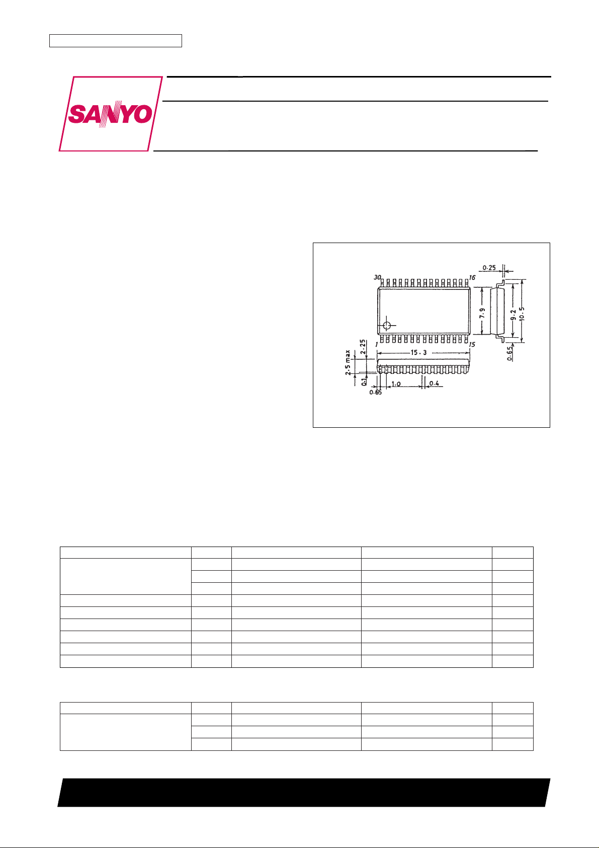
Package Dimensions
unit: mm
3073A-MFP30S
SANYO: MFP30S
[LB1881M]
Specifications
Absolute Maximum Ratings at Ta = 25°C
Parameter Symbol Conditions Ratings Unit
V
CC
1 max 7 V
Supply voltage V
CC
2 max 12 V
V
S
max VCC2V
Output applied voltage V
O
max VS+ 2 V
Input applied voltage V
I
max All input pins VCC1V
Output current I
O
max 1.0 A
Allowable power dissipation Pd max 1.0 W
Operating temperature T
opr
–20 to +75 °C
Storage temperature T
stg
–55 to +150 °C
Allowable Operating Ranges at Ta = 25°C
Parameter Symbol Conditions Ratings Unit
V
CC
1VCC1 ≤ VCC2 4.0 to 6.0 V
Supply voltage V
CC
2 4 to 10 V
V
S
Up to VCC2V
No. 4455-2/6
LB1881M
Electrical Characteristics at Ta = 25°C, VCC1 = 5 V, VCC2 = 7 V, VS= 3 V
Ratings
Parameter Symbol Conditions
min typ max
Unit
I
CC
1 VBR= 5 V 3.0 5.0 mA
Supply current I
CC
2 VBR= 5 V 6.5 10.0 mA
I
S
VBR= 5 V, RL= ∞ 5.0 mA
Output quiescent current
I
CCOQ
V
STBY
= 0 V 100 µA
I
SOQ
V
STBY
= 0 V, RL= ∞ 150 µA
Output saturation voltage V
O(sat)
I
OUT
= 0.6 A, sink + source 1.7 V
Output TRS withstand voltage V
O(sus)
I
OUT
= 20 mA*1 12 V
Output quiescent voltage V
OQ
VBR= 5 V 1.45 1.55 1.65 V
Hall amplifier input offset voltage V
HOFFSET
*1 –5 +5 mV
Hall amplifier common mode input
V
HCOM
1.4 2.8 V
voltage range
Hall I/O voltage gain GV
HO
Rangle = 8.2 kΩ 34.0 37.0 40.0 dB
Brake pin high level voltage V
BRH
2.0 V
Brake pin low level voltage V
BRL
0.8 V
Brake pin input current I
BRIN
120 µA
Brake pin leakage current I
BRLEAK
–30 µA
FRC pin high level voltage V
FRCH
2.8 V
FRC pin low level voltage V
FRCL
1.2 V
FRC pin input current I
FRCIN
100 µA
FRC pin leakage current I
FRCLEAK
–30 µA
Upper side residual voltage V
XH
I
OUT
= 100 mA, VCC2 = 6 V, VS= 2 V 0.285 0.455 V
Lower side residual voltage V
XL
I
OUT
= 100 mA, VCC2 = 6 V, VS= 2 V 0.350 0.440 V
Residual voltage inflection point V
S∆VX
I
OUT
= 100 mA, VCC2 = 6 V*1 0.9 V
Overlap level OL V
CC
2 = 6 V, VS= 3 V, RL= 100 Ω (Y) 60 70 80 %
Overlap vertical difference ∆OL V
CC
2 = 6 V, VS= 3 V, RL= 100 Ω (Y) –10 0 +10 %
Standby on voltage V
STBYL
*2 –0.2 +0.8 V
Standby off voltage V
STBYH
2 5 V
Standby pin bias current I
STBYIN
100 µA
Thermal protection circuit operating
T
TSD
*1 150 180 210 °C
temperature
Thermal protection circuit hysteresis ∆T
TSD
*1 15 °C
FG amplifier input offset voltage V
FG OFFSET
–8 +8 mV
Open loop voltage gain GV
FG
f = 10 kHz 43 dB
Source output saturation voltage V
FG OU
IO= –2 mA 3.7 V
Sink output saturation voltage V
FG OD
IO= 2 mA 1.3 V
Common mode signal exclusion ratio G
HR
*1 80 dB
FG amplifier common mode input
V
FG CH
0 3.5 V
voltage range
Phase margin φM *1 20 deg
Schmitt amplifier threshold voltage V
FGS SH
V
FGIN
+
= 2.5 V,
2.45 2.50 2.55 V
when V
FGOUT
2 goes from high to low
Schmitt amplifier hysteresis width V
FGS HIS
V
FGIN
+
= 2.5 V 20 40 60 mV
Note: 1. These are target settings, and are not measured. The overlap ratings are taken as test ratings without change.
2. When the standby pin is open the IC will be in the standby state.
 Loading...