

SANYO LB1876 Datasheet
Ordering number : ENN6201A
61202RM (OT)/62599RM (KI) No. 6201-1/14
Overview
The LB1876 is a driver for polygon mirror motors such as
used in laser printers and similar equipment.
It incorporates all necessary circuitry (speed control +
driver) on a single chip. Direct PWM drive enables drive
with low power loss.
Functions and Features
• Three-phase bipolar drive
• Direct PWM drive technique
• Built-in lower side output diode
• Output current limiter
• Reference clock input circuit (FG frequency equivalent)
• PLL speed control circuit
• Phase lock detector output (with masking function)
• Built-in protection circuitry includes current limiter,
restraint protection, overheat protection, low-voltage
protection, etc.
• Brake method switching circuit (free-run or reverse
torque)
• 5V regulator output
• Power save function
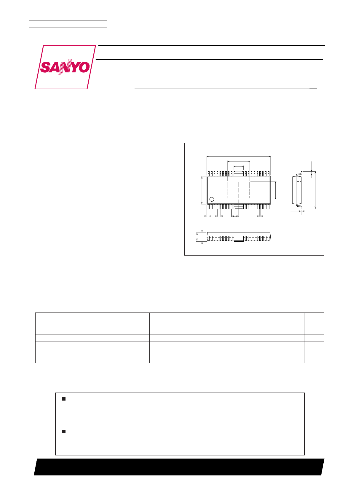
Package Dimensions
unit: mm
3235A-HSOP36
(6.2)
36
1
0.8
17.8
2.7
0.3
(4.9)
10.5
0.65
0.25
(0.5)
7.9
(2.25)
2.45max
0.1
2.0
SANYO: HSOP36
[LB1876]
LB1876
SANYO Electric Co.,Ltd. Semiconductor Company
TOKYO OFFICE Tokyo Bldg., 1-10, 1 Chome, Ueno, Taito-ku, TOKYO, 110-8534 JAPAN
Three-Phase Brushless Motor Driver
for Polygon Mirror Motors
Monolithic Digital IC
Any and all SANYO products described or contained herein do not have specifications that can handle
applications that require extremely high levels of reliability, such as life-support systems, aircraft’s
control systems, or other applications whose failure can be reasonably expected to result in serious
physical and/or material damage. Consult with your SANYO representative nearest you before using
any SANYO products described or contained herein in such applications.
SANYO assumes no responsibility for equipment failures that result from using products at values that
exceed, even momentarily, rated values (such as maximum ratings, operating condition ranges, or other
parameters) listed in products specifications of any and all SANYO products described or contained
herein.
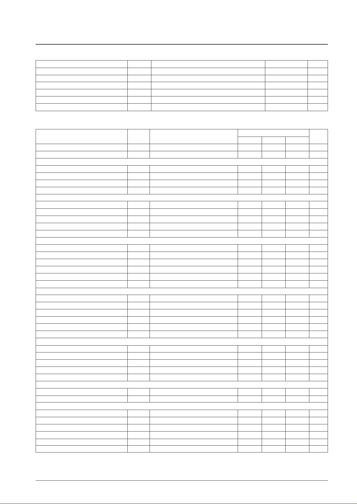
Parameter Symbol Conditions Ratings Unit
Maximum supply voltage 1 V
CC
max 30 V
Maximum output current I
O
max T ≤ 500 ms 2.5 A
Allowable power dissipation 1 Pd max1 IC only 0.9 W
Allowable power dissipation 2 Pd max2 *With substrate 2.1 W
Operating temperature Topr –20 to +80 °C
Storage temperature Tstg –55 to +150 °C
Specifications
Maximum Ratings at Ta = 25°C
* Substrate: 114.3 × 76.1 × 1.6 mm3, glass epoxy
No. 6201-2/14
LB1876
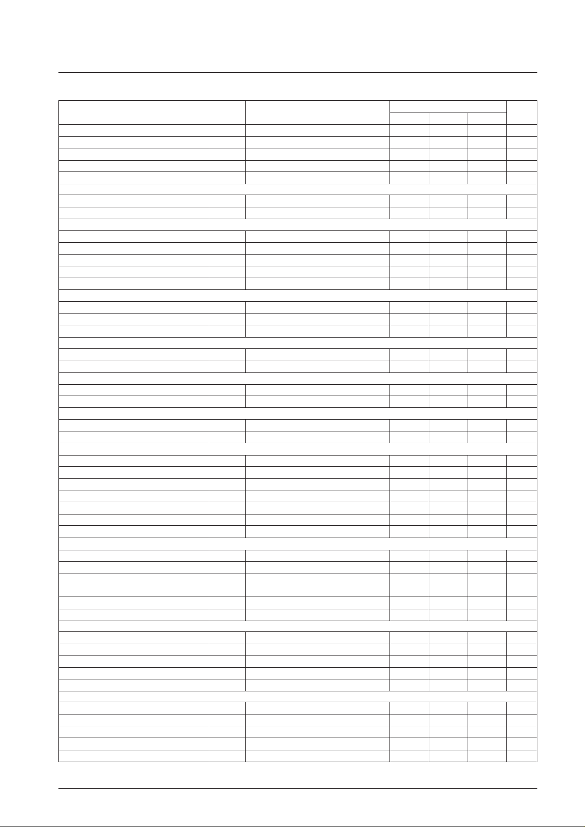
Parameter Symbol Conditions
Ratings
Unit
min typ max
Power supply current 1 I
CC
1 17 22 mA
Power supply current 2 I
CC
2 Quiescent Current 3.6 5.0 mA
[5V regulated output]
Output voltage VREG 4.65 5.0 5.35 V
Voltage fluctuation ∆VREG1 V
CC
= 9.5 to 28 V 50 100 mV
Load fluctuation ∆VREG2 I
O
= –5 to –20 mA 30 100 mV
Temperature coefficcient ∆VREG3 Design target value 0 mV/°C
[Output block]
Output saturation voltage 1 V
O
sat1 IO= 1.0 A, VO(SINK)+VO(SOURCE) 2.0 2.5 V
Output saturation voltage 2 V
O
sat2 IO= 2.0 A, VO(SINK)+VO(SOURCE) 2.6 3.2 V
Output leak current I
O
leak 100 µA
Lower side diode forward voltage 1 VD1 ID = –1.0 A 1.2 1.5 V
Lower side diode forward voltage 2 VD2 ID = –2.0 A 1.5 1.9 V
[Hall amplifier block]
Input bias current IHB –2 –0.5 µA
Common mode input voltage range VICM 0
VREG – 2.0
V
Hall input sensitivity 80 mVp–p
Hysteresis width ∆V
IN
(HA) 15 24 42 mV
Input voltage L → H VSLH 12 mV
Input voltage H → L VSHL –12 mV
[FG/Schmitt block]
Input bias current IB(FGS) –2 –0.5 µA
Common mode input voltage range
VICM(FGS)
0
VREG – 2.0
V
Input sensitivity V
IN
(FGS) 80 mVp–p
Hysteresis width
∆VIN(FGS)
15 24 42 mV
Input voltage L → H
VSLH(FGS)
12 mV
Input voltage H → L
VSHL(FGS)
–12 mV
[PWM oscillator]
Output High level voltage
VOH(PWM)
2.5 2.8 3.1 V
Output Low level voltage
VOL(PWM)
1.2 1.5 1.8 V
External capacitor charge current ICHG VPWM = 2 V –125 –95 –75 µA
Oscillator frequency f(PWM) C = 3000 pF 22 kHz
Amplitude V(PWM) 1.05 1.27 1.50 Vp-p
[FGS output]
Output saturation voltage V
O
L(FGS) IFGS = 7 mA 0.15 0.5 V
Output leak current IL(FGS) 10 µA
[CSD oscillator]
Output High level voltage
VOH(CSD)
2.65 3.0 3.3 V
Output Low level voltage
VOL(CSD)
0.75 0.9 1.1 V
Amplitude V(CSD) 1.75 2.1 2.3 Vp–p
External capacitor charge current ICHG1 –13.5 –9 –5.5 µA
External capacitor discharge current ICHG2 5.5 9 13.5 µA
Oscillator frequency f(CSD) C = 0.068 µF 30 Hz
Electrical Characteristics at Ta = 25°C, VCC= VM = 24 V
Parameter Symbol Conditions Ratings Unit
Power supply voltage range V
CC
9.5 to 28 V
5 V regulated output current IREG 0 to –20 mA
LD pin voltage VLD 0 to 28 V
LD pin output current ILD 0 to 15 mA
FGS pin voltage VFGS 0 to 28 V
FGS pin output current IFGS 0 to 10 mA
Allowable Operating Ranges at Ta = 25°C
Continued on next page.
No. 6201-3/14
LB1876
Continued from preceding page.
Parameter Symbol Conditions
Ratings
Unit
min typ max
[Phase comparator output]
Output High level voltage VPDH I
O
H = –100 µA
VREG-0.2 VREG-0.1
V
Output Low level voltage VPDL I
O
H = 100 µA 0.2 0.3 V
Output source current IPD+ VPD = VREG/2 –0.5 mA
Output sink current IPD– VPD = VREG/2 1.5 mA
[Phase lock detector output]
Output saturation voltage V
O
L(LD) ILD = 10 mA 0.15 0.5 V
Output leak current IL(LD) V
O
= V
CC
10 µA
[ERR amplifier]
Input offset voltage V
I
O(ER) Design target value –10 +10 mV
Input bias current I
B
(ER) –1 +1 µA
Ouput High level voltage V
O
H(ER) IOH = –500 µA
VREG–1.2 VREG-0.9
V
Ouput Low level voltage V
O
L(ER) IOL = 500 µA 0.9 1.2 V
DC bias level VB(ER) –5% VREG/2 +5% V
[Current limiter]
Drive gain 1 GDF1 in phase lock mode 0.4 0.5 0.6 times
Drive gain 2 GDF2 in unlock mode 0.8 1.0 1.2 times
Limiter voltage VRF V
CC
- V
M
0.45 0.5 0.55 V
[Thermal shutdown operation]
Termal shutdown operating temperature TSD Design target value (junction temperature) 150 180 °C
Hysteresis width ∆TSD Design target value (junction temperature) 40 °C
[Low voltage protection]
Operating voltage VSD 8.1 8.5 8.9 V
Hysteresis ∆VSD 0.2 0.35 0.5 V
[CLD circuit]
External capacitor charge current ICLD –6 –4.3 –3 V
Operating voltage VH(CLD) 3.25 3.5 3.75 V
[CLK pin]
External input frequency fI(CKIN) 0.1 10 kHz
High level input voltage V
I
H(CKIN) 3.5 VREG V
Low level input voltage V
I
L(CKIN) 0 1.5 V
Input open voltage V
I
O(CKIN)
VREG-0.5
VREG V
Hysteresis width V
I
S(CKIN) 0.35 0.5 0.65 V
High level input current I
I
H(CKIN) VCKIN = VREG –10 0 +10 µA
Low level input current I
I
L(CKIN) VCKIN = 0 V –280 –210 µA
[S/S pin]
High level input voltage V
I
H(SS) 3.5 VREG V
Low level input voltage V
I
L(SS) 0 1.5 V
Input open voltage V
I
O(SS)
VREG-0.5
VREG V
Hysteresis width V
I
S(SS) 0.35 0.5 0.65 V
High level input current I
I
H(SS) VS/S = VREG –10 0 +10 µA
Low level input current I
I
L(SS) VS/S = 0 V –280 –210 µA
[LDSEL pin]
High level input voltage
VIH(LD
SEL
)
3.5 VREG V
Low level input voltage
VIL(LD
SEL
)
0 1.5 V
Input open voltage
VIO(LD
SEL
)
VREG-0.5
VREG V
High level input current
IIH(LD
SEL
)
V
LDSEL
= VREG –10 0 10 µA
Low level input current
IIL(LD
SEL
)
V
LDSEL
= 0 V –280 –210 µA
[BRSEL pin]
High level input voltage
VIH(BR
SEL
)
3.5 VREG V
Low level input voltage
VIL(BR
SEL
)
0 1.5 V
Input open voltage
VIO(BR
SEL
)
VREG-0.5
VREG V
High level input current
IIH(BR
SEL
)
V
LDSEL
= VREG –10 0 10 µA
Low level input current
IIL(BR
SEL
)
V
LDSEL
= 0 V –280 –210 µA

Three-phase logic truth table (IN = "H" indicates the IN+ > IN– condition)
No. 6201-4/14
LB1876
IN1 IN2 IN3 OUT1 OUT2 OUT3
H L H L H M
H L L L M H
H H L M L H
L H L H L M
L H H H M L
L L H M H L
Pin Assignment
LB1876
35
LDSEL
BRSEL
GND3
34
OUT3
NC
33 32 31 30 29 2836 27 26 25 24 23 22 21 20 19
VM1
VM2
V
CC
VREG
FGS
LD
S/S
CLK
EO
EI
PD
CLD
TOC
FGFIL
FRAME
FC
PH
CSD
GND1
FGIN-
PWM
GND2
FGIN+
FRAME
IN2-
IN2+
IN1-
IN1+
NC
OUT1
IN3-
IN3+
OUT2
Top view
0.4
0
0.8
0.9
1.2
1.6
2.0
2.1
2.4
–20 0 20 40 60 80 100
Pd max — Ta
1.18
Ambient temperature, Ta — ºC
With substrate (114.3 × 76.1 × 1.6 mm
3
, glass epoxy)
Power dissipation, Pd max — W
IC independent
987654321
10 11 12 13 14 15 16 17 18
No. 6201-5/14
LB1876
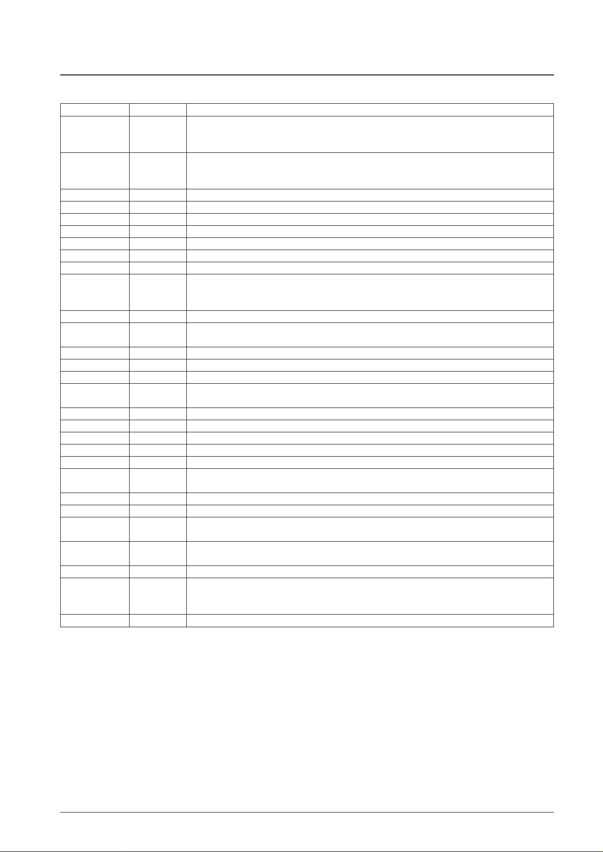
Pin Description
Pin name Pin number Function
OUT1 2
OUT2 1
OUT3 36
IN1+, IN1– 8, 9
IN2+, IN2– 6, 7
IN3+, IN3– 4, 5
FG IN+ 10 FG comparator non-inverting input.
FG IN– 11 FG comparator inverting input.
GND1 12 Control circuit ground.
GND2 13 Sub-ground.
PWM 14 PWM oscillation frequency setting pin. Connect to ground via capacitor.
FC 15 Current control circuit frequency characteristics compensation pin. Connect to ground via capacitor.
FGFIL 16 FG filter pin. Connect to ground via capacitor if noise in FG signal is a problem.
CSD 17
PH 18 RF waveform smoothing pin. Connect to ground via capacitor.
TOC 19
EO 20 Error amplifier output.
EI 21 Error amplifier input.
PD 22 Phase comparator output pin. Phase deviation is output as a duty cycle change of the pulse.
CLD 23
FGS 24 FG Schmitt output (open collector output).
LD 25 Phase lock detector output (open collector output). Goes ON when PLL is locked.
S/S 26 Start/stop input. Low: Start; High or Open: Stop.
CLK 27 Clock input. 10 kHz max.
VM1 28 Output block power supply. Short to VM2 for use.
VM2 29
VCC 30 Power supply pin. Connect to ground via capacitor to prevent noise.
VREG 31 5V regulator output pin (control circuit power supply). Connect to ground via capacitor to stabilize operation.
LDSEL 32
BRSEL 33
GND3 34 Output circuit ground.
FRAME —
NC 3, 35 Not connected internally. Can be used for wiring.
Output pins.
PWM controls duty cycle ratio by lower transistors.
Connect Schottky diode between these pins and VCC.
Hall input pins for each phase.
Logic High indicates VIN+ > VIN–.
Restraint protection circuit operating time setting pin/reset pulse setting pin.
Connect to ground via capacitor. If the protection circuit is not to be used, connect a resistor in parallel
with capacitor.
Torque specifying input pin. Normally connected to EO pin. When TOC potential falls, ON duty cycle ratio of
lower side output transistors changes and torque increases.
Phase lock signal masking time setting pin. Connect to ground via capacitor. Leave open if masking is not
required.
Output current detector pin. Connect to VCC via low resistor.
Set to maximum output current IOUT = 0.5/Rf.
Phase lock signal masking switching pin. When "Low", the unlock signal (short "High" signal of LD output) is
masked. When "High" or Open, the lock signal (short "Low" signal of LD output) is masked.
Braking method select pin. "Low" selects reverse torque control and "High" or Open selects free-run.
When reverse torque is controlled, lower side output transistors require external SBD.
The FRAME pin is connected internally to the metal frame at the base of the IC. Electrically, both the FRAME
pin and the metal frame are left open. To improve thermal dissipation, provide a corresponding land on the
PCB and solder the FRAME pin to that land.
 Loading...