

SANYO LB1872 Datasheet
Overview
The LB1872 is a 3-phase brushless motor driver IC
developed for driving the polygon mirror motor used in
laser printers and similar products.
Functions and Features
• Integrates the circuits (speed control and driver circuits)
required for laser printer polygon mirror motor drive in a
single chip.
• Uses a current linear drive technique for minimal motor
noise. Only a small capacitors are required for output
oscillation prevention.
• PLL speed control adopted for high-precision rotation
with excellent jitter characteristics.
• Phase lock detection output with a chattering prevention
function
• Four rotation rates can be set up using a single crystal
oscillator to support 240, 300, 400, and 600 dpi
operation.
• Arbitrary rotation rates can be acquired when an
external clock is used.
• Deceleration function implemented by short-circuit
braking (free running when stopped)
• Built-in FG and error amplifiers
• Full complement of protection circuits, including
thermal protection, low voltage protection, and current
limiter circuits, provided on chip.
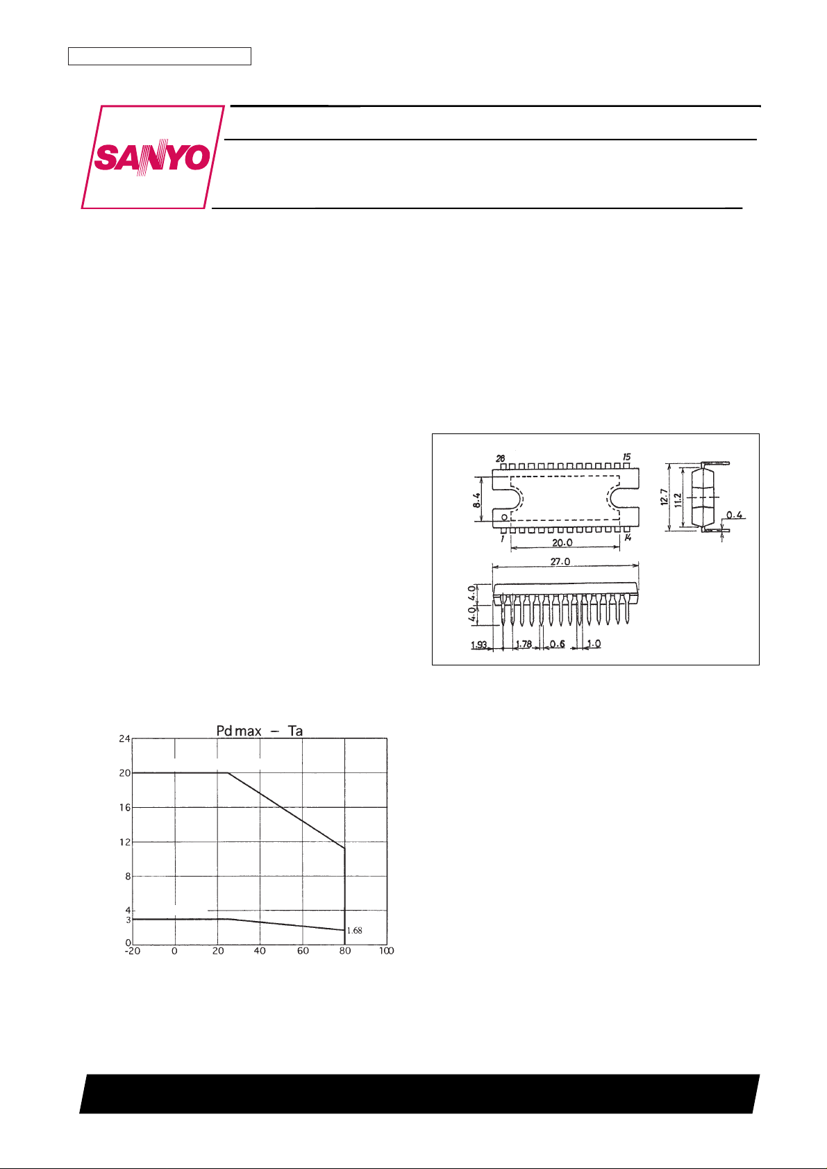
Package Dimensions
unit: mm
3147B-DIP28H
Monolithic Digital IC
13098HA(OT) No. 5625-1/11
SANYO: DIP28H
[LB1872]
SANYO Electric Co.,Ltd. Semiconductor Bussiness Headquarters
TOKYO OFFICE Tokyo Bldg., 1-10, 1 Chome, Ueno, Taito-ku, TOKYO, 110-0005 JAPAN
Polygon Mirror Scanner Driver IC
LB1872
Ordering number : EN5625A
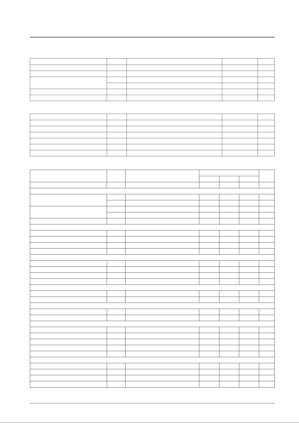
Independent IC
Ambient temperature, Ta - °C
Allowable power dissipation, Pd max - W
With an arbitrarily large heat sink
No. 5625-2/11
LB1872
Parameter Symbol Conditions
Ratings
Unit
min typ max
Current drain I
CC
In stop mode 20 27 mA
[Output Saturation Voltage] V
AGC
= 2 V
Source
V(sat)1-1 I
O
= 0.7 A, RF= 0 Ω 1.5 1.9 V
V(sat)1-2 I
O
= 1.5 A, RF= 0 Ω 1.8 2.2 V
Sink
V(sat)2-1 I
O
= 0.7 A, RF= 0 Ω 0.3 0.5 V
V(sat)2-2 I
O
= 1.5 A, RF= 0 Ω 0.7 1.0 V
Output leakage current I
O
(leak) VCC= 28 V 100 µA
[5-V Fixed-Voltage Output]
Output voltage V
REG
4.65 5.0 5.35 V
Voltage regulation ∆V
REG
1 VCC= 10 to 28 V 40 100 mV
Load regulation ∆V
REG
2 IO= 0 to 10 mA 20 100 mV
Temperature coefficient ∆V
REG
3 Design target value 0 mV/°C
[Hall Input Block]
Input bias current I
B(HA)VAGC
= 3 V 2 10 µA
Differential-mode input range V
HIN
With a sine wave input 50 350 mV
Common-mode input range V
ICM
Differential input: 50 mV p-p 3.5 VCC– 3.5 V
Input offset voltage V
IOH
Design target value –20 +20 mV
[Low Voltage Protection Circuit]
Operating voltage V
SD
8.4 8.8 9.2 V
Hysteresis ∆V
SD
0.2 0.4 0.6 V
[Thermal Protection Circuit]
Shutdown temperature TSD Design target value (junction temperature) 150 180 °C
Hysteresis ∆TSD Design target value (junction temperature) 40 °C
[FG Amplifier]
Input offset voltage V
IO(FG)
Design target value –10 +10 mV
Input bias current I
B(FG)
–1 +1 µA
DC bias level V
B(FG)
–5% 1/2V
REG
+5% V
Output high-level voltage V
OH(FG)IOH
= –500 µA V
REG
– 1.2 V
REG
– 0.8 V
Output low-level voltage V
OL(FG)IOL
= 500 µA 0.8 1.2 V
[FG Schmitt Input Block]
Input hysteresis (high to low) V
SHL
0 mV
Input hysteresis (low to high) V
SLH
150 mV
Hysteresis V
FGL
100 150 200 mV
Input operating level V
FGSIL
400 mV
Electrical Characteristics at Ta = 25°C, VCC= 24 V
Parameter Symbol Conditions Ratings Unit
Supply voltage V
CC
10 to 28 V
5.0-V fixed-voltage output current I
REG
0 to –15 mA
LD pin voltage V
LD
0 to 28 V
FGS pin voltage V
FGS
0 to 28 V
LD pin output current I
LD
0 to 10 mA
FGS pin output current I
FGS
0 to 5 mA
Allowable Operating Ranges at Ta = 25°C
Parameter Symbol Conditions Ratings Unit
Maximum supply voltage V
CC
max 30 V
Maximum output current I
O
max t ≤0.5s 2.0 A
Allowable power dissipation
Pd max1 Independent IC 3 W
Pd max2 Arbitrarily large heat sink 20 W
Operating temperature Topr –20 to +80 °C
Storage temperature Tstg –55 to +150 °C
Specifications
Absolute Maximum Ratings at Ta = 25°C
Continued on next page.
No. 5625-3/11
LB1872
Continued from preceding page.
Parameter Symbol Conditions
Ratings
Unit
min typ max
Output saturation voltage V
FGS(sat)IFGS
= 3 mA 0.2 0.4 V
Output leakage current I
L(FGS)VCC
= 28 V 10 µA
[Error Amplifier]
Input offset voltage V
IO(ER)
Design target value –10 +10 mV
Input bias current I
B(ER)
–1 +1 µA
DC bias level V
B(ER)
–5% 1/2V
REG
+5% V
Output high-level voltage V
OH(ER)IOH
= –500 µA V
REG
– 1.2 V
REG
– 0.8 V
Output low-level voltage V
OL(ER)IERI
= 100 µA, IOL= 500 µA 0.7 1.0 1.3 V
[Phase Comparator Output]
Output high-level voltage V
PDHIOH
= –100 µA V
REG
– 0.2 V
REG
– 0.1 V
Output low-level voltage V
PDLIOL
= 100 µA 0.1 0.2 V
Output source current I
PD
+ VPD= V
REG
/2 –0.6 mA
Output sink current I
PD
– VPD= V
REG
/2 1.5 mA
[Lock Detection Output]
Output saturation voltage V
LD(sat)ILD
= 5 mA 0.1 0.4 V
Output leakage current I
LDLEAKVCC
= 28 V 10 µA
[Drive Block]
Output idling voltage V
ID
6 mV
Forward gain
G
DF
1 When the phase is locked 0.4 0.5 0.6
G
DF
2 When unlocked 2.4 3.0 3.6
Current limiter V
L
Rf = 2 Ω 0.45 0.5 0.55 V
Brake command voltage V
BRK
2.3 V
[Reference Signal Block]
Crystal oscillator frequency f
OSC
In crystal oscillator mode 1 10 MHz
Low-level pin voltage V
OSCLIOSC
= –0.5 mA 1.7 V
High-level pin voltage I
OSCHVOSC
= V
OSCL
+ 0.3 V 0.5 mA
[N1 Pin]
External input frequency f
I
(N1) In external clock mode 100 10000 Hz
High-level input voltage V
IH
(N1) 3.5 V
REG
V
Low-level input voltage V
IL
(N1) 0 1.5 V
Input open voltage V
IO
(NI) V
REG
– 0.5 V
REG
V
Hysteresis V
IS
(N1) 0.3 0.4 0.5 V
High-level input current I
IH
(N1) VN1 = V
REG
–10 0 +10 µA
Low-level input current I
IL
(N1) VN1 = 0 V –350 –275 µA
[N2 Pin]
High-level input voltage V
IH
(N2) 4.0 V
REG
V
Middle-level input voltage V
IM
(N2) 2.0 3.0 V
Low-level input voltage V
IL
(N2) 0 1.0 V
Input open voltage V
IO
(N2) 2.2 2.5 2.8 V
High-level input current I
IH
(N2) VN2 = V
REG
200 270 µA
Low-level input current I
IL
(N2) VN2 = 0 V –270 –200 µA
[S/S Pin]
High-level input voltage V
IH
(SS) 3.5 V
REG
V
Low-level input voltage V
IL
(SS) 0 1.5 V
Input open voltage V
IO
(SS) V
REG
– 0.5 V
REG
V
Hysteresis V
IS
(SS) 0.3 0.4 0.5 V
High-level input current I
IH
(SS) VS/S = V
REG
–10 0 +10 µA
Low-level input current I
IL
(SS) VS/S = 0 V –350 –275 µA
[CLD Pin]
Charge current I
CLD
1 V
CLD
= 0 V (Phase locked) –9 –7 –5 µA
Discharge current I
CLD
2 VCL= V
REG
/2 (Phase unlocked) 1 mA
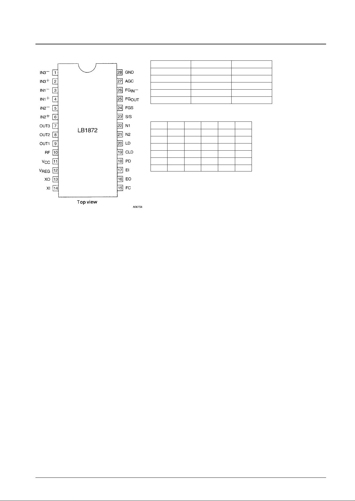
Pin Assignment
No. 5625-4/11
LB1872
Clock Divisor Switching
N1 N2 Divisor
H H 2048 (4
× 1 × 512)
H L 4096 (4 × 2 × 512)
L H 5120 (5 × 2 × 512)
L L 3072 (3 × 2 × 512)
CLK IN M or open EXT. CLK
Three-Phase Logic Truth Table
H1 H2 H3 OUT1 OUT2 OUT3
H L H L H M
H L L L M H
H H L M L H
L H L H L M
L H H H M L
L L H M H L
 Loading...