

SANYO LB1868 Datasheet
Ordering number : ENN*6202
LB1868
Two-Phase Brushless Fan Motor Driver
Preliminary
Overview
The LB1868 is a 2-phase unipolar brushless motor driver.
With only a few peripheral parts, lockup protection and
automatic recovery can be implemented. The IC can be
configured for 12V or 24V operation and a wide range of
variations, from LOW speed to H-High speed and from 60
cm to 120 cm square using the same PCB. This makes it
easy to design highly reliable fan motor installations.
Functions and Features
• Output protection Zener diode with variable withstand
voltage
Z1, Z2 pins open: VOLM = 57V (24V specification)
Z1, Z2 pins shorted: VOLM = 32V (12V specification)
External Zener diode connected across Z1 - VCC pins:
support for fans with large drive current
• External resistor allows configuration for 12V or 24V.
• Direct Hall element connection possible (built-in Hall
amplifier with hysteresis supports core without auxiliary
electrode)
• Built-in output transistor with 1.0A output current
(strengthened negative-current support for core without
auxiliary electrode)
• Built-in rotation detection function: Low during rotation
and High during stop
• Built-in lockup protection with automatic recovery
• Built-in thermal shutdown
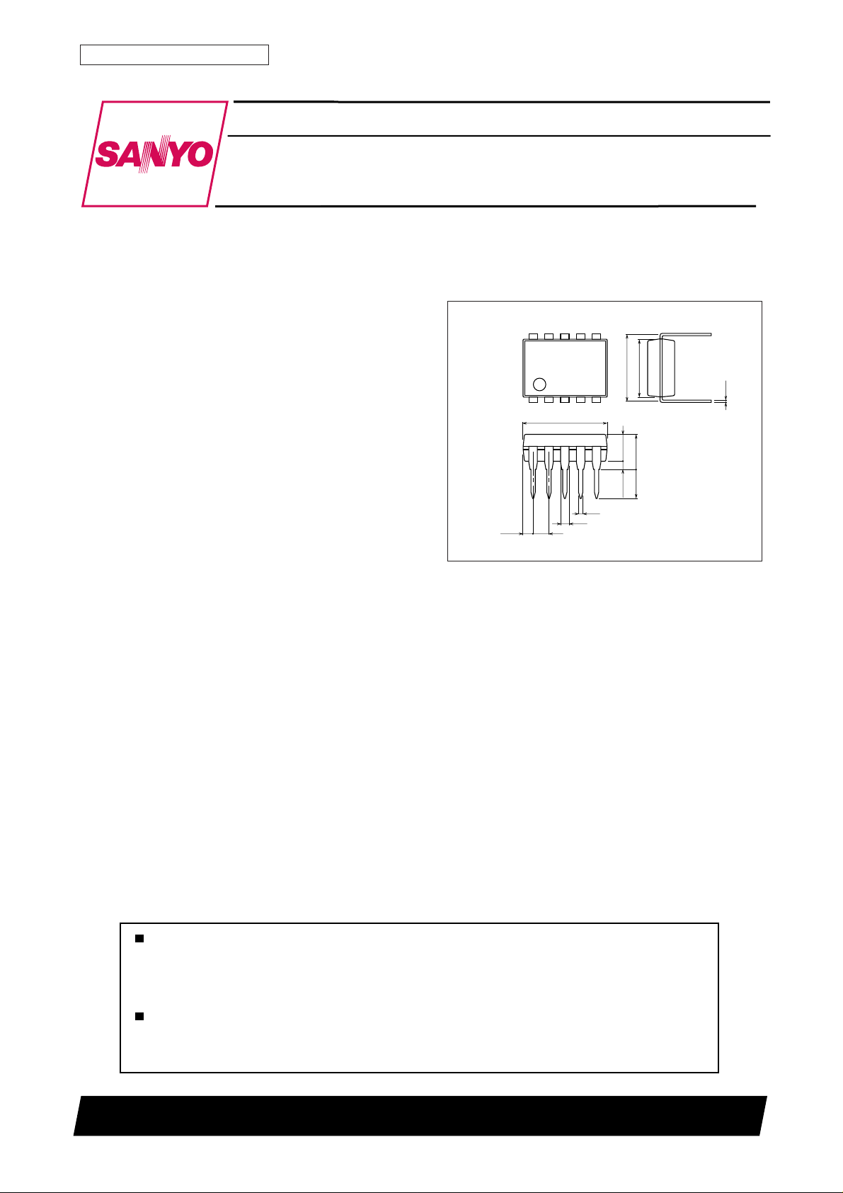
Package Dimensions
unit: mm
3098B-DIP10S
[LB1868]
10
1
1.14 1.78
9.4
0.95
6
5
0.48
Monolithic Digital IC
LB1868
6.4
7.62
3.0
3.9max
3.2
0.51min
SANYO : DIP10S
0.25
Any and all SANYO products described or contained herein do not have specifications that can handle
applications that require extremely high levels of reliability, such as life-support systems, aircraft's
control systems, or other applications whose failure can be reasonably expected to result in serious
physical and/or material damage. Consult with your SANYO representative nearest you before using
any SANYO products described or contained herein in such applications.
SANYO assumes no responsibility for equipment failures that result from using products at values that
exceed, even momentarily, rated values (such as maximum ratings, operating condition ranges, or other
parameters) listed in products specifications of any and all SANYO products described or contained
herein.
SANYO Electric Co.,Ltd. Semiconductor Company
TOKYO OFFICE Tokyo Bldg., 1-10, 1 Chome, Ueno, Taito-ku, TOKYO, 110-8534 JAPAN
83100RM(KI)
No. 6202-1/4
LB1868
Specifications
Absolute Maximum Ratings at Ta = 25˚C
Parameter Symbol Conditions Ratings Unit
Maximum input current ICC max t ≤ 20 ms 200 mA
Maximum applied output voltage VOUT max Internal V
Maximum output current IOUT max 1.0 A
Current flowing into RD pin IRD max 10 mA
RD applied voltage VRD max 30 V
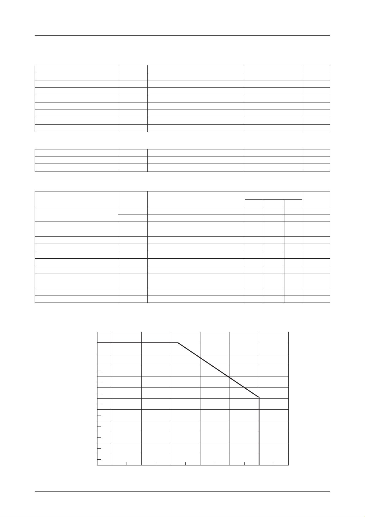
Allowable power dissipation Pd max 1.1 W
Operating temperature Topr –30 to +80 °C
Storage temperature Tstg –55 to +150 °C
Allowable Operating Ranges at Ta = 25˚C
Parameter Symbol Conditions Ratings Unit
Input voltage range ICC 6.0 to 50 mA
Common mode input voltage range VICM 0.2 to VIN–1.5 V
Electrical Characteristics at Ta = 25˚C, Icc = 10 mA
Parameter Symbol Conditions
Output limiter withstand voltage VOLM1 Z1, Z2 open 54 57 60 V
VOLM2 Z1, Z2 short 31 33 35 V
Output saturation voltage Vosat 1 Io = 0.5A 0.95 1.2 V
2 Io = 1.0A 0.15 1.5 V
VIN voltage VIN ICC = 7.0 mA 6.4 6.7 7.0 V
Hall input sensitivity (at zero peak) VHN Including offset and hysteresis 20 mV
RD output saturation voltage VRDsat IRD = 5 mA 0.1 0.3 V
CT drain current IC1 C = GND 2.7 3.8 4.9 µA
CT discharge current IC2 C = VIN 0.19 0.30 0.41 µA
Comp input threshold voltage VTH1 0.77
VTH2 0.42
Thermal protection operating temperature
Thermal protection circuit hysteresis ∆TSD Design target value* 40 °C
TSD Design target value* 180 °C
* Design target values are not measured.
Ratings
min typ max
0.8VIN
0.45VIN
0.83 V
0.48 V
Unit
Pd max – Ta
1. 1
1. 0
0. 9
0. 8
0. 7
0. 6
0. 5
0. 4
0. 3
0. 2
Allowable power dissipation, Pd max – W
0. 1
0
Ambient temperature, Ta – °C
100806040200–20–30
No. 6202-2/4
 Loading...