

SANYO LB1862M Datasheet
Overview
The LB1862M is a single-phase full-wave driver provided
in a miniature package that is optimal for driving
miniature fans such as CPU cooling fans. It provides
motor drive with low switching noise and high efficiency.
Functions
• Supports both 5- and 12-V power supplies.
• Allows the use of reverse connection prevention diodes
by including a regeneration circuit on chip.
• On-chip Hall amplifier with hysteresis characteristics
(Supports commutator-free cores.)
• Lock protection and automatic recovery circuits
• Lock detection pin
(Latch type – Low: drive, High: stopped)
• Supports low current drain in standby mode by
providing a Hall bias pin and a start/stop pin.
• Thermal shutdown circuit
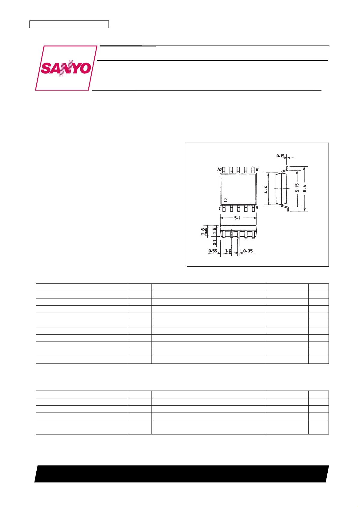
Package Dimensions
unit: mm
3086A-MFP10S
Monolithic Digital IC
Ordering number : EN5657
73097HA(OT) No. 5657-1/6
SANYO: MFP10S
SANYO Electric Co.,Ltd. Semiconductor Bussiness Headquarters
TOKYO OFFICE Tokyo Bldg., 1-10, 1 Chome, Ueno, Taito-ku, TOKYO, 110 JAPAN
Single-Phase Full-Wave Driver for Fan Motors
LB1862M
Parameter Symbol Conditions Ratings Unit
Supply voltage V
CC
max 17 V
Output current I
OUT
max 0.5 A
Output voltage V
OUT
max 15 V
RD output voltage V
R
max 15 V
RD output current I
R
max 5mA
HB output current I
B
max 10 mA
ST input voltage V
ST
max 15 V
Allowable power dissipation Pd max When mounted on the specified board * 850 mW
Operating temperature Topr –20 to +75 °C
Storage temperature Tstg –55 to +150 °C
Specifications
Absolute Maximum Ratings at Ta = 25°C
Note: * Specified board: 114.3 × 76.2 × 1.5 mm epoxy glass laminate board
Parameter Symbol Conditions Ratings Unit
Supply voltage V
CC
3.8 to 16.8 V
ST input high-level voltage ST
H
3 to 14 V
ST input low-level voltage ST
L
–0.3 to +0.4 V
Hall input
V
ICM
0.2 to VCC–1.5 V
common-mode input voltage range
Allowable Operating Ranges at Ta = 25°C
[LB1862M]
No. 5657-2/6
LB1862M
Parameter Symbol Conditions
Ratings
Unit
min typ max
During drive operation (CT = low, ST = low) 6.5 9.1 mA
Current drain I
CC
During lock protection (CT = high, ST = low) 2.2 3.1 mA
Standby mode (ST = high) 110 150 µA
Lock detection capacitor charge current I
CT
1 1.9 2.8 3.7 µA
Capacitor discharge current I
CT
2 0.32 0.46 0.60 µA
Capacitor charge/discharge current ratio R
CT
RCD= ICT1/ICT2 5.0 6.0 7.0
CT charge voltage V
CT
1 2.55 2.75 2.95 V
CT discharge voltage V
CT
2 1.6 1.8 2.0 V
Output low-level voltage V
OLIO
= 200 mA 0.2 0.3 V
Output high-level voltage V
OHIO
= 200 mA 3.9 4.1 V
Hall input sensitivity V
HN
Zero peak value
7 15 mV
(Including the offset and hysteresis.)
RD output pin low-level voltage V
RDIRD
= 5 mA 0.1 0.3 V
RD output pin leakage current I
RDLVRD
= 15 V 30 µA
HB output low-level voltage V
HBLIHB
= 5 mA 1.0 1.3 V
ST pin input current I
ST
VST= 5 V 75 100 µA
Electrical Characteristics at Ta = 25°C, VCC= 5 V
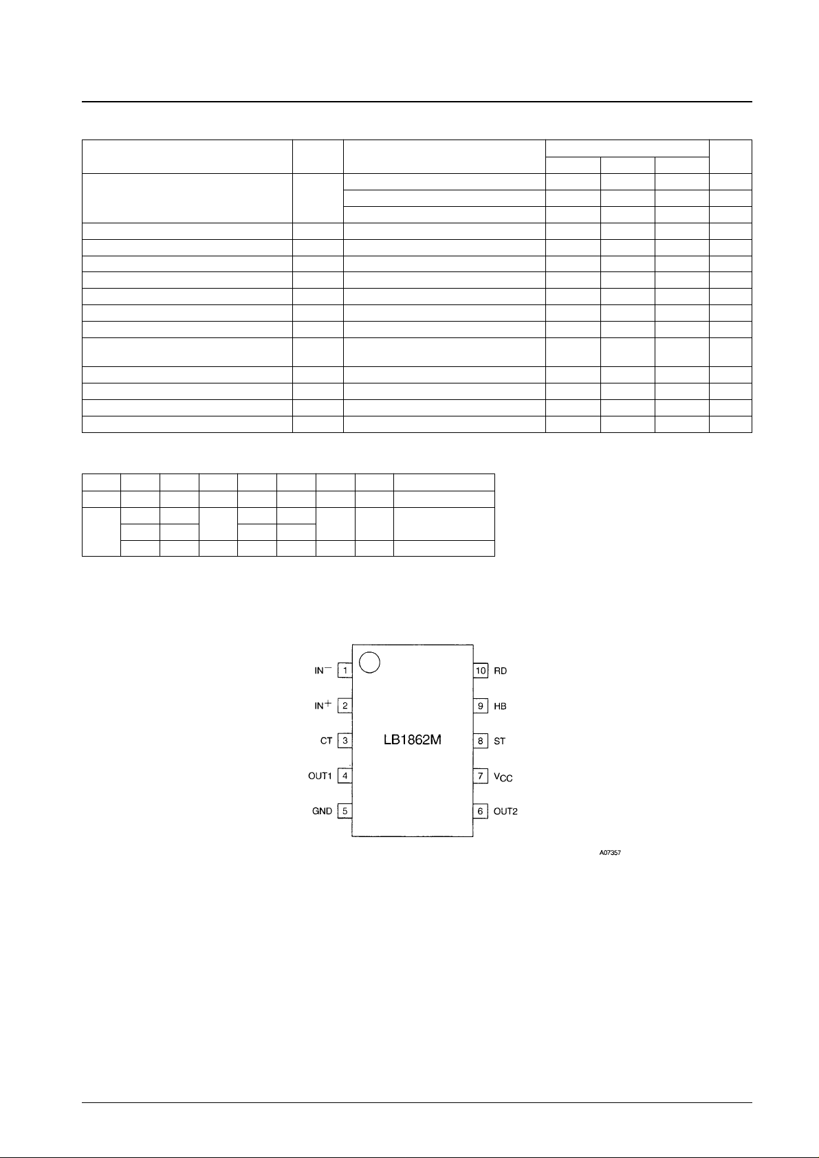
Truth Table
Pin Assignment
The RD output is a latch-type output; Low: drive, High: stopped
ST IN
–
IN
+
CT OUT1 OUT2 RD HB Mode
H — — — off off off off Standby
H L
L
H L
L L Drive
L L H L H
H off off off L Lock protection
Top view
 Loading...