

Page 1
Ordering number : ENN6208A
LB1862
Monolithic Digital IC
LB1862
Fan Motor Single-Phase Full-Wave Driver
Overview
Single-phase full-wave drive design and a compact package
make this IC optimal for small fans (especially CPU
cooling fans). Low switching noise and effective motor
drive are further advantages.
Features
• Support for 5V/12V dual power supply voltage
• Built-in regenerative circuit allows use of reverseconnection protection diode
• Built-in Hall amplifier with hysteresis (supports core
without auxiliary electrode)
• Built-in lockup protection and automatic recovery circuits
• Latch-type lockup detection output (RD) is Low during
rotation and High during stop
• Hall bias pin and start/stop pin allow reduced current drain
in standby mode
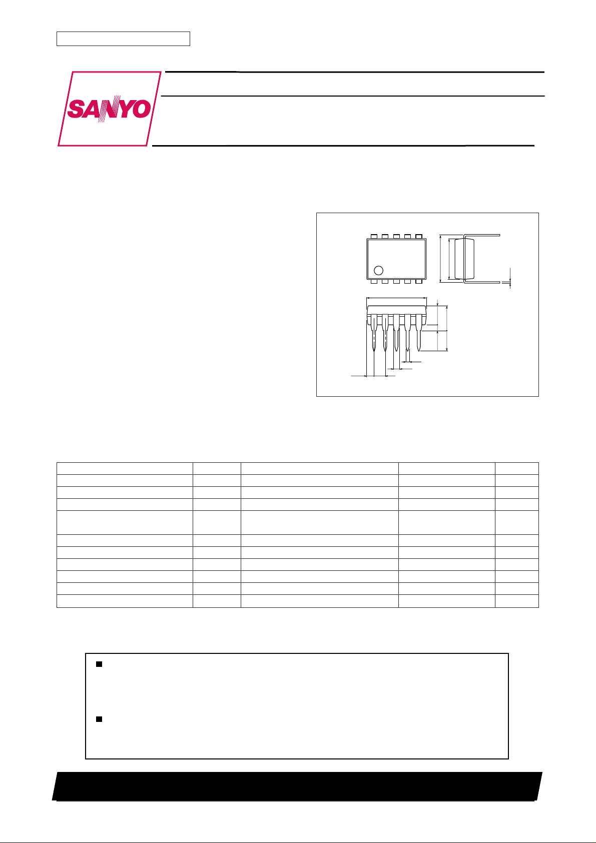
Package Dimensions
unit: mm
3098B-DIP10S
[LB1862]
10
1
1.14 1.78
9.4
0.95
6
5
0.48
6.4
7.62
3.0
3.9max
3.2
0.51min
0.25
SANYO : DIP10S
• Built-in thermal protection circuit
Specifications
Absolute Maximum Ratings at Ta = 25˚C
Parameter Symbol Conditions Ratings Unit
Maximum supply voltage VCC max 17 V
Maximum output current I
Maximum output withstand voltage V
RD maximum output withstand
voltage
RD maximum output current IR max 5mA
HB maximum output current IB max 10 mA
ST maximum input voltage VST max 15 V
Allowable power dissipation Pd max 1.0 W
Operating temperature Topr –30 to +85 °C
Storage temperature Tstg –55 to +150 °C
max 0.8 A
OUT
max 17 V
OUT
VR max
17 V
Any and all SANYO products described or contained herein do not have specifications that can handle
applications that require extremely high levels of reliability, such as life-support systems, aircraft's
control systems, or other applications whose failure can be reasonably expected to result in serious
physical and/or material damage. Consult with your SANYO representative nearest you before using
any SANYO products described or contained herein in such applications.
SANYO assumes no responsibility for equipment failures that result from using products at values that
exceed, even momentarily, rated values (such as maximum ratings, operating condition ranges, or other
parameters) listed in products specifications of any and all SANYO products described or contained
herein.
SANYO Electric Co.,Ltd. Semiconductor Company
TOKYO OFFICE Tokyo Bldg., 1-10, 1 Chome, Ueno, Taito-ku, TOKYO, 110-8534 JAPAN
O2599RM(KI)
No. 6208-1/7
Page 2
LB1862
Allowable Operating Ranges at Ta = 25˚C
Parameter Symbol Conditions Ratings Unit
Power supply voltage V
ST input High level voltage ST
ST input Low level voltage ST
Hall input common mode input
voltage range
CC
H
L
V
ICM
Electrical Characteristics at Ta = 25˚C, VCC = 5V
Parameter Symbol Conditions
Circuit current I
In drive mode (CT = [L], ST = [L]) 6.5 9.1 mA
CC
In lockup protection mode (CT = [H], ST = [L])
In standby mode (ST = [H]) 110 150 µA
Lockup detection ICT1 1.9 2.8 3.7 µA
capacitor charge current
Capacitor discharge current ICT2 0.32 0.46 0.60 µA
Capacitor charge/discharge current ratio
R
RCT = ICT1/ICT2 5.0 6.0 7.0
CT
CT charge voltage VCT1 2.55 2.75 2.95 V
CT discharge voltage VCT2 1.6 1.8 2.0 V
Output Low level voltage V
Output High level voltage V
Hall input sensitivity V
IO = 200 mA 0.2 0.3 V
OL
OHIO
HN
= 200 mA 3.9 4.1 V
Zero peak value 7 15 mV
(Including offset and hysteresis)
RD output pin Low voltage V
RD output pin leakage current I
HB output Low voltage V
ST pin input current I
RDL
IRD = 5 mA 0.1 0.3 V
RD
VRD = 15V 30 µA
HBLIHB
ST
= 5 mA 1.0 1.3 V
VST = 5V 75 100 µA
min typ max
3.8 to 16.8 V
3 to 14 V
–0.3 to +0.4 V
0.2 to VCC–1.5 V
Ratings
2.2 3.1 mA
Unit
1.2
1.0
0.8
0.6
0.4
0.2
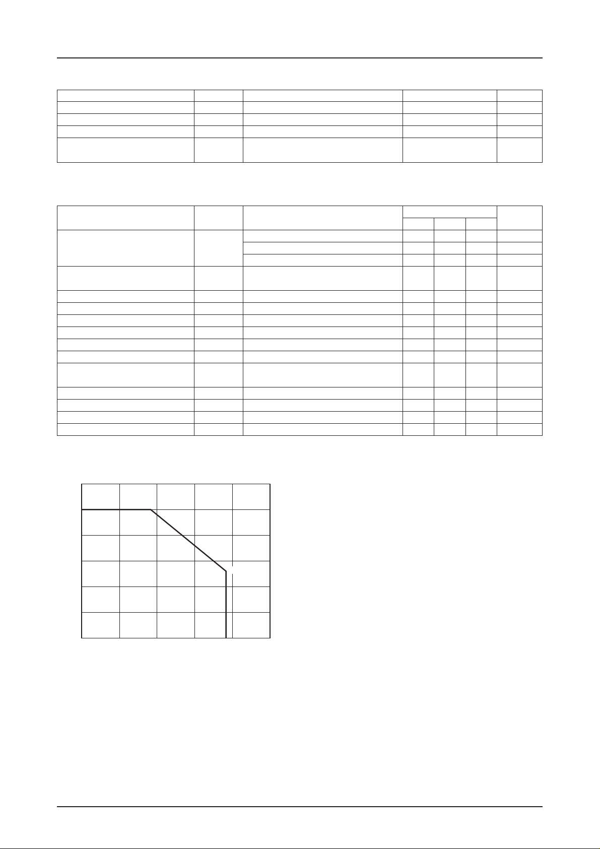
Pd max – Ta
0.52
Allowable power dissipation, Pd max – W
0
–30 0 30 60 90 120
Ambient temperature, Ta – °C
No. 6208-2/7
Page 3
LB1862
Truth Table
ST IN
H – – – off off off off Standby
LLH LH
–
HL
Pin Assignment
+
IN
CT OUT1 OUT2 RD HB Mode
L
H off off off L Lockup protection activated
HL
Latch-type RD output is Low during rotation and High during stop.
L L Rotating
IN
IN
CT
OUT1
GND
–
1
+
2
3
4
5
LB1862
10
RD
9
HB
8
ST
7
V
CC
6
OUT2
Top view
A12476
No. 6208-3/7
Page 4

Block Diagram
LB1862
0.47 to 1µF
HALL
CT
Discharge
V
CC
+
IN
–
IN
HB
pulse
Hysteresis amplifier
Thermal protection
circuit
Control
circuit
Charge/discharge
circuit
Delay circuit
Delay circuit
START/STOP
ST GND
RD
OUT2
M
OUT1
A12478
Sample Application Circuit
C2
C1=0.47 to 1µF
D1
V
CC
H
–
IN
RD
+
IN
OUT1
HB
OUT2
ST
CT
GND
A12477
(1) D1 is used to prevent IC destruction caused by reverse-connection. It can be omitted if no problems are expected.
(2) C2 would not be required for the internal fan PCB but required for the power supply line in order to reduce the
power line inpedance and pass the regenerative current because a motor is basically an inductive load and it has a
possibility of large current when the power is first applied or in other cases.
(3) When CT is not used, it should be connected to ground.
(4) When RD, ST, and HB are not used, they should be left open or connected to ground.
No. 6208-4/7
Page 5

Startup
LB1862
Startup
V
CC
OUT
CT
RD
Power-on
Lockup protection/automatic recovery
A12479
Start/stop
OUT
RD
CT
ST
OUT
Locked Released
Output OFF
Output OFF
Output ON
Output OFF
RD
A12480
No. 6208-5/7
Page 6

LB1862
Design reference
(1) VCC pin
Power supply pin for control block and motor drive.
Accepts a wide operation voltage range from 3.8 to 16.8V, for 5V/12V dual power supply support.
(2) OUT1, OUT2 pins
Single-phase coil output pins.
Bipolar drive output with upper side inverted and lower side single output. Built-in regenerative circuit regenerates
kickback current between lower side NPN outputs when a diode is used for protection against IC destruction caused
by reverse connection.
(3) IN–, IN+ pins
Hall input signal pins
The Hall signal is amplified into a square wave by the Hall amplifier with hysteresis characteristics of ±3.5 mV
(typ.). The Hall input signal amplitude should be 70 mV or more.
(4) CT pin
This pin serves for connecting a capacitor between CT and GND.
The capacitor determines the characteristics of the built-in lockup protection circuit for preventing coil burnout in
the case of motor restraint. Once normal motor load is restored, the automatic recovery circuit resets itself.
Changing the capacitance alters the lockup detection time.
When a 0.47 µF capacitor is connected between CT and GND
Lockup detection time : approx. 0.5s
Lockup protection time/automatic recovery time : approx. 0.16s (output ON)
approx. 1s (output OFF)
When not using lockup protection function, this pin should be connected to ground.
(5) RD pin
Open-collector output pin that is Low during rotation and OFF when lockup is detected.
The output is a latch type which stays OFF also when the automatic recovery circuit has restored drive mode, unless
the rotation actually resumes.
(6) ST pin and HB pin
ST pin : When input to this pin is High, motor drive is stopped (OUT is high impedance).
At this time, RD output indicates lockup protection mode OFF.
HB pin : Hall bias switching pin. At ST pin High input, Hall bias is cut off to reduce current drain in fan standby
mode.
If not used, both pins should be open.
(7) Thermal protection circuit
When internal temperature Tj of IC reaches 180°C, output current limiter is activated to protect against damage.
No. 6208-6/7
Page 7

LB1862
Specifications of any and all SANYO products described or contained herein stipulate the performance,
characteristics, and functions of the described products in the independent state, and are not guarantees
of the performance, characteristics, and functions of the described products as mounted in the customer's
products or equipment. To verify symptoms and states that cannot be evaluated in an independent device,
the customer should always evaluate and test devices mounted in the customer's products or equipment.
SANYO Electric Co., Ltd. strives to supply high-quality high-reliability products. However, any and all
semiconductor products fail with some probability. It is possible that these probabilistic failures could
give rise to accidents or events that could endanger human lives, that could give rise to smoke or fire,
or that could cause damage to other property. When designing equipment, adopt safety measures so
that these kinds of accidents or events cannot occur. Such measures include but are not limited to protective
circuits and error prevention circuits for safe design, redundant design, and structural design.
In the event that any or all SANYO products(including technical data,services) described or
contained herein are controlled under any of applicable local export control laws and regulations,
such products must not be exported without obtaining the export license from the authorities
concerned in accordance with the above law.
No part of this publication may be reproduced or transmitted in any form or by any means, electronic or
mechanical, including photocopying and recording, or any information storage or retrieval system,
or otherwise, without the prior written permission of SANYO Electric Co. , Ltd.
Any and all information described or contained herein are subject to change without notice due to
product/technology improvement, etc. When designing equipment, refer to the "Delivery Specification"
for the SANYO product that you intend to use.
Information (including circuit diagrams and circuit parameters) herein is for example only ; it is not
guaranteed for volume production. SANYO believes information herein is accurate and reliable, but
no guarantees are made or implied regarding its use or any infringements of intellectual property rights
or other rights of third parties.
This catalog provides information as of October, 1999. Specifications and information herein are subject to change
without notice.
No. 6208-7/7
PS
 Loading...