

SANYO LB1847 Datasheet
Ordering number : EN5982
1
14
28
15
0.4
0.6
4.04.0
27.0
20.0
R1.7
8.4
1.93 1.78
1.0
12.7
11.2
LB1847
Monolithic Digital IC
LB1847
PWM Current Control Type Stepping Motor Driver
Overview
The LB1847 is a driver IC for stepping motors with
PWM current control bipolar drive (fixed OFF
time). A special feature of this IC is that V
REF
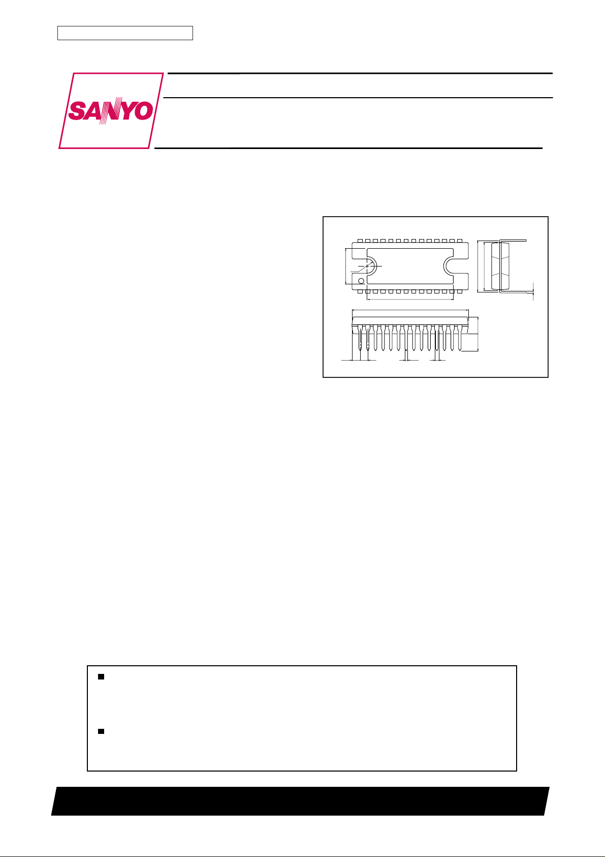
Package Dimensions
unit: mm
3147B-DIP28H
voltage is constant while the current can be set in
15 steps, allowing drive of motors ranging from 12 phase exciter types to 4W 1-2 phase exciter
types. The current decay pattern can also be
selected (SLOW DECAY, FAST DECAY, MIX
DECAY) to increase the decay of regenerative
current at chopping OFF, thereby improving
response characteristics. This is especially useful
for carriage and paper feed stepping motors in
printers and similar applications where highprecision control and low vibrations are required.
Features
• PWM current control (fixed OFF time)
• Load current digital selector (1-2, W1-2, 2W1-2, 4W1-2 phase exciter drive possible)
• Selectable current decay pattern (SLOW DECAY, FAST DECAY, MIX DECAY)
• Simultaneous ON prevention function (feedthrough current prevention)
• Noise canceler
• Built-in thermal shutdown circuit
• Built-in logic low-voltage OFF circuit
[LB1847]
SANYO : DIP28H
Any and all SANYO products described or contained herein do not have specifications that can handle
applications that require extremely high levels of reliability, such as life-support systems, aircraft's
control systems, or other applications whose failure can be reasonably expected to result in serious
physical and/or material damage. Consult with your SANYO representative nearest you before using
any SANYO products described or contained herein in such applications.
SANYO assumes no responsibility for equipment failures that result from using products at values that
exceed, even momentarily, rated values (such as maximum ratings, operating condition ranges, or other
parameters) listed in products specifications of any and all SANYO products described or contained
herein.
SANYO Electric Co., Ltd. Semiconductor Business Headquarters
TOKYO OFFICE Tokyo Bldg., 1-10, 1 Chome, Ueno, Taito-ku, TOKYO, 110-8534 JAPAN
11499RM(KI)
No. 5982-1/16

LB1847
Specifications
Maximum Ratings at Ta = 25°C
Parameter Symbol Conditions Ratings Unit
Motor supply voltage 50 V
Output peak current 1.75 A
Output continuous current 1.5 A
Logic supply voltage 7.0 V
Logic input voltage range V
Emitter output voltage 1.0 V
Allowable power dissipation Pd max Ta=25°C 3.0 W
Operating temperature range Topr °C
Storage temperature range Tstg °C
Allowable Operating Ranges at Ta = 25°C
Parameter Symbol Conditions Ratings Unit
Motor supply voltage range 10 to 45 V
Logic supply voltage range 4.75 to 5.25 V
Reference voltage range 0.0 to 3.0 V
V
BB
I
OPEAK
IO max
V
CC
V
IN
V
E
V
BB
V
CC
V
REF
tW≤20 µs
–0.3 to V
CC
With heat sink 20 W
–20 to +85
–55 to +150
25
Pd max – Ta
With an arbitrary large heat sink
20
15
10
5
IC only
Allowable power dissipation, Pdmax – W
0
0–20 20 40 60 80 100
3.0
Ambient temperature, Ta – ˚C
20.0
10.4
1.56
No. 5982-2/16
LB1847
Electrical Characteristics at Ta = 25°C, V
Parameter Symbol Conditions
= 45V, V
BB
= 5V, V
CC
REF
= 1.52V
Ratings
min typ max
[Output Block]
Output stage supply voltage 2.3 3.5 5.0 mA
Output saturation voltage 1.2 1.6 V
Output leak current 50 µA
Output sustain voltage 45 V
I
BB ON
IBB
OFF
VO(sat)1
(sat)2
V
O
V
(sat)3
O
VO(sat)4
IO(leak)1
IO(leak)2
V
SUS
IO=+1.0A, sink
I
=+1.5A, sink
O
I
=–1.0A, source
O
IO=–1.5A, source
VO=VBB, sink
VO=0V, source
L=15 mH, IO=1.5A, Guaranteed design value
0.5 0.8 1.1 mA
1.5 1.9 V
1.9 2.2 V
2.2 2.4 V
–50 µA
[Logic Block]
Logic supply voltage 19.5 26 36.5 mA
Input voltage 3.2 V
Input current 100 µA
Sensing voltage 0.470 0.525 V
Reference current –0.5 µA
CR pin current CR=1.0V –4.6 –1.0 mA
MD pin current MD=1.0V, CR=4.0V –5.0 µA
DECAY pin current Low –10 µA
DECAY pin current High 5 µA
I
CC ON
I
CC OFF
V
IH
V
I
IH
I
IL
V
E
I
REF
I
CR
I
MD
I
DECL
I
DECH
I4=3.2V, I3=3.2V, I2=3.2V, I1=3.2V
ENABLE=3.2V 10.5 15 19.5 mA
IL
VIH=3.2V
VIL=0.8V
I4=3.2V, I3=3.2V, I2=3.2V, I1=3.2V
I
=3.2V, I3=3.2V, I2=3.2V, I1=0.8V
4
I4=3.2V, I3=3.2V, I2=0.8V, I1=3.2V
=3.2V, I3=3.2V, I2=0.8V, I1=0.8V
I
4
I
=3.2V, I3=0.8V, I2=3.2V, I1=3.2V
4
I4=3.2V, I3=0.8V, I2=3.2V, I1=0.8V
I4=3.2V, I3=0.8V, I2=0.8V, I1=3.2V
=3.2V, I3=0.8V, I2=0.8V, I1=0.8V
I
4
=0.8V, I3=3.2V, I2=3.2V, I1=3.2V
I
4
I4=0.8V, I3=3.2V, I2=3.2V, I1=0.8V
I4=0.8V, I3=3.2V, I2=0.8V, I1=3.2V
I4=0.8V, I3=3.2V, I2=0.8V, I1=0.8V
I4=0.8V, I3=0.8V, I2=3.2V, I1=3.2V
=0.8V, I3=0.8V, I2=3.2V, I1=0.8V
I
4
V
=1.5V
REF
V
=0.8V
DEC
V
=3.2V
DEC
–10 µA
0.50
0.445 0.48 0.505 V
0.425 0.46 0.485 V
0.410 0.43 0.465 V
0.385 0.41 0.435 V
0.365 0.39 0.415 V
0.345 0.37 0.385 V
0.325 0.35 0.365 V
0.280 0.3 0.325 V
0.30
0.240 0.26 0.285 V
0.195 0.22 0.235 V
0.155 0.17 0.190 V
0.115 0.13 0.145 V
0.075 0.09 V
0.8 V
0.190
0.100
Thermal shutdown temperature TSD 170 °C
Logic ON voltage 3.35 3.65 3.95 V
Logic OFF voltage 3.20 3.50 3.80 V
L
hysteresis width
VSD
L
∆L
L
VSD
VSD
VSD
1
2
0.065 0.15 0.23 V
Unit
No. 5982-3/16
LB1847
Truth table
PHASE ENABLE
HLHL
LLLH
HOFFOFF
Set current truth table
I
IA4IA3
1111 100
1110 95.65
1101 91.30
1100 86.95
1011 82.61
1010 78.26
1001 73.91
1000 69.56
0111 60.87
0110 52.17
0101 43.48
0100 34.78
0011 26.08
0010 17.39
* Current ratio (%) is the calculated set current value.
2
I
A
A
1
11.5/11.5 X V
11.0/11.5 X V
10.5/11.5 X V
10.0/11.5 X V
9.5/11.5 X V
9.0/11.5 X V
8.5/11.5 X V
8.0/11.5 X V
7.0/11.5 X V
6.0/11.5 X V
5.0/11.5 X V
4.0/11.5 X V
3.0/11.5 X V
2.0/11.5 X V
OUT
A
OUT
A
Set current Iout Current ratio (%)
/3.04RE=Iout
REF
/3.04RE=Iout
REF
/3.04RE=Iout
REF
/3.04RE=Iout
REF
/3.04RE=Iout
REF
/3.04RE=Iout
REF
/3.04RE=Iout
REF
/3.04RE=Iout
REF
/3.04RE=Iout
REF
/3.04RE=Iout
REF
/3.04RE=Iout
REF
/3.04RE=Iout
REF
/3.04RE=Iout
REF
/3.04RE=Iout
REF
Current decay switching truth table
Current decay mode DECAY pin MD pin Output chopping
SLOW DECAY H L Top-side chopping
FAST DECAY L L Dual-side chopping
MIX DECAY
L
4V to 1.5V input
voltage setting
CR voltage > MD : dual-side chopping
CR voltage < MD : top-side chopping
No. 5982-4/16

LB1847
Pin function
Pin number Pin name Function description
1
2 Output set current reference supply pin
13 Setting voltage range: 0V to 3V
3 CR1
12 CR2
4E1
11 E2
5 DECAY1 SLOW mode/FAST mode selector pin
10 DECAY2 SLOW DECAY: H
6
7
8
9
14 Output stage supply voltage pin
15 GND Ground pin
27 PHASE1
16 PHASE2
26 ENABLE1
17 ENABLE2
22, 23
24, 25 Output set current digital input pin
21, 20 15-stage voltage setting
19, 18
28 Logic block supply voltage pin
M D
V
REF
V
REF
OUT
OUT
OUT
OUT
V
BB
IA4, IA3
I
2, IA1
A
4, IB3
I
B
I
2, IB1
B
V
CC
Sets the OFF time for FAST mode and SLOW mode in MIX DECAY
Setting input range: 4V to 1.5V
1
2
Output OFF time setting pin for switching operation
Pin for controlling the set current with sensing resistor RE
FAST DECAY: L
A
A
B
B
Output pin
Output phase selector input pin
Output ON/OFF setting input pin
Pin Assignment
VCCPHASE1
1282273264
MD
1
REF
V
1
2
3
4
4
3
2
A
ENABLE1
I
A
A
A
B
I
I
I
B
I
I
1
B
B
I
I
ENABLE2
2552462372282192010191118121713161415
LB1847
CR1
E1
DECAY1
A
OUT
OUTAOUTBOUT
B
DECAY2
E2
CR2
PHASE2
2
REF
V
A11312
GND
BB
V
Top view
No. 5982-5/16
 Loading...