SANYO LB1845 Datasheet

Overview
The LB1845 is a PWM current control type stepping
motor driver that uses a bipolar drive scheme. It is
particularly suitable for driving carriage and paper feed
stepping motors in printers and similar products.
Features
• PWM current control (fixed off time scheme)
• Digital load current selection function
• Sustained output voltage: 45 V
• Built-in thermal shutdown circuit
Package Dimensions
unit: mm
3147A-DIP28H
Monolithic Digital IC
Ordering number: EN5505B
D3096HA (OT) No. 5505-1/7
SANYO: DIP28H
[LB1845]
SANYO Electric Co.,Ltd. Semiconductor Bussiness Headquarters
TOKYO OFFICE Tokyo Bldg., 1-10, 1 Chome, Ueno, Taito-ku, TOKYO, 110 JAPAN
PWM Current Control Stepping Motor Driver
LB1845
Parameter Symbol Conditions Ratings Unit
Motor supply voltage V
BB
45 V
Peak output current I
OPEAKtW
= 20 µS 1.75 A
Continuous output current I
OMAX
1.5 A
Logic block supply voltage V
CC
7.0 V
Logic input voltage range V
IN
–0.3 to V
CC
V
Emitter output voltage V
E
1.0 V
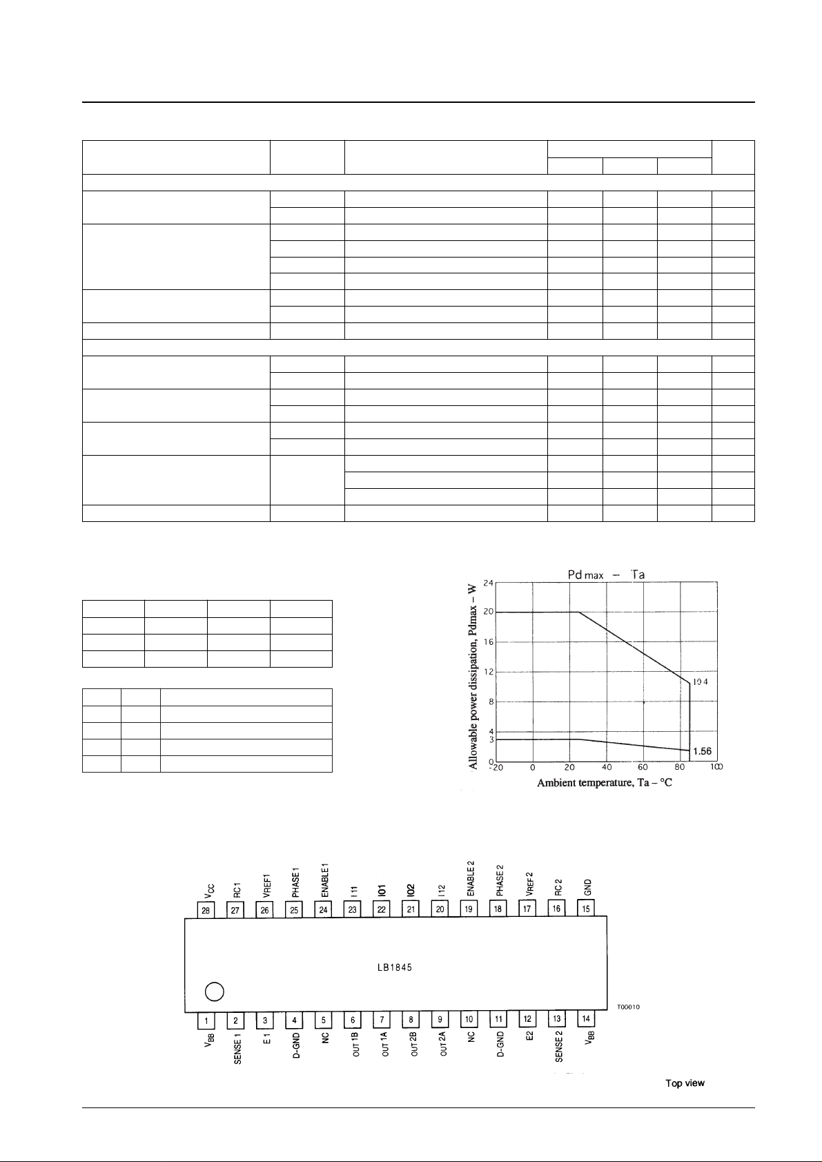
Allowable power dissipation
Pd max1 Independent IC 3.0 W
Pd max2 With an arbitrarily large heat sink 20.0 W
Operating temperature Topr –20 to +85 °C
Storage temperature Tstg –55 to +150 °C
Specifications
Absolute Maximum Ratings at Ta = 25°C
Parameter Symbol Conditions Ratings Unit
Motor supply voltage V
BB
10 to 44.5 V
Logic block supply voltage V
CC
4.75 to 5.25 V
Reference voltage V
REF
1.5 to 7.5 V
Recommended Operating Ranges at Ta = 25°C

No. 5505-2/7
LB1845
Parameter Symbol Conditions
Ratings
Unit
min typ max
[Output Block]
Output stage supply voltage
I
BB ON
12 16 mA
I
BB OFF
0.7 0.9 mA
V
O
(sat)1 IO= +1.0 A sink 1.2 1.4 V
Output saturation voltage 1
V
O
(sat)2 IO= +1.5 A sink 1.4 1.7 V
V
O
(sat)3 IO= –1.0 A source 1.1 1.3 V
V
O
(sat)4 IO= –1.5 A source 1.3 1.6 V
Output leakage current
I
O
(leak)1 VO= VBBsink 50 µA
I
O
(leak)2 VO= 0 V source –50 µA
Sustained output voltage V(sus) * 45 V
[Logic Block]
Logic supply current
I
CC ON
I0 = 0.8 V, I1 = 0.8 V 19.5 25.3 mA
I
CC OFF
I0 = 2.4 V, I1 = 2.4 V 15.5 20.1 mA
Input voltage
V
IH
2.4 V
V
IL
0.8 V
Input current
I
IH
VIH= 2.4 V 10 µA
I
IL
VIL= 0.8 V –10 µA
I0 = 0.8 V, I1 = 0.8 V 9.5 10 10.5
Current control threshold voltage V
REF/VSENSE
I0 = 2.4 V, I1 = 0.8 V 13.5 15 16.5
I0 = 0.8 V, I1 = 2.4 V 25.5 30 34.5
Thermal shutdown temperature T
S
170 °C
Electrical Characteristics at Ta = 25°C, VBB= 38 V, VCC= 5 V, V
REF
= 5 V
Truth Table
Pin Assignment
Note: *Design guaranteed value
Note: Outputs go off when ENABLE is high or in the I0 = I1 = high state.
ENABLE PHASE OUT A OUT B
L H H L
L L L H
H — OFF OFF
I0 I1 Output current
L L V
REF
/ (10 × RE) = I
OUT
H L V
REF
/ (15 × RE) = I
OUT
× 2/3
L H V
REF
/ (30 × RE) = I
OUT
× 1/3
H H 0

Block Diagram
Application Circuit Diagram
No. 5505-3/7
LB1845
 Loading...