

SANYO LB1832V Datasheet
Ordering number : EN4179A
41596HA (OT) No. 4179-1/7
Overview
The LB1832V is a bidirectional driver IC that includes an
on-chip low-voltage low-saturation 1.5-channel bridge and
is provided in a miniature package. It is therefore optimal
for cameras that use 3 V lithium batteries. This IC allows
direct drive from the control microprocessor and supports
control of standby, forward, reverse, and braking
operations for two motors, i.e. the film take-up and lens
drive motors, from three inputs.
Features
• Supports low-voltage drive.
— When the same power supply is used for VCCand
VS: VCC= VS= 1.6 V min.
— When different power supplies are used for VCCand
VS: VS= 1.0 V min, VCC= 2.5 V min.
• Low saturation voltage (Upper side transistor plus lower
side transistor remaining voltage: 0.6 V (typ) at 1 A)
• Zero current drain in standby mode
• 1.5-channel bidirectional driver that can be directly
driven from the control microprocessor
• Separate logic and motor power supply connections
• Brake function
• Built-in spark killer diode
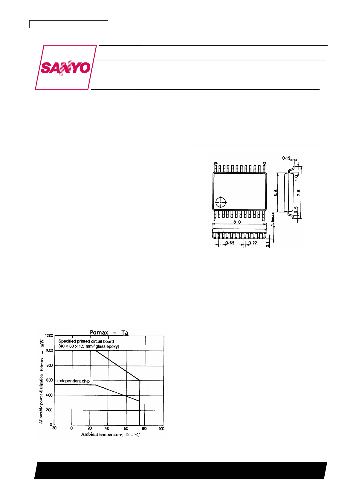
• Miniature package (SSOP-24)
Package Dimensions
unit: mm
3175A-SSOP24
SANYO: SSOP24
[LB1832V]
LB1832V
SANYO Electric Co.,Ltd. Semiconductor Bussiness Headquarters
TOKYO OFFICE Tokyo Bldg., 1-10, 1 Chome, Ueno, Taito-ku, TOKYO, 110-0005 JAPAN
Low-Saturation 1.5-Channel 3 V Drive
Bidirectional Driver
Monolithic Digital IC
Specifications
Absolute Maximum Ratings at Ta = 25°C
Allowable Operating Ranges at Ta = 25°C
Electrical Characteristics at Ta = 25°C, VCC= VS= 3 V
No. 4179-2/7
LB1832V
Parameter Symbol Conditions Ratings Unit
Maximum supply voltage
V
CC
max –0.3 to +8.0 V
V
S
max –0.3 to +8.0 V
Output applied voltage V
OUT
–0.3 to VS+ V
SF
V
Input applied voltage V
IN
–0.3 to +0.8 V
GND pin current I
GND
2.0 A
Pd max1 Independent IC 550 mW
Allowable power dissipation
Pd max2
Mounted on the specified printed circuit board
1000 mW
(40
× 30 × 1.5 mm3glass epoxy)
Operating temperature Topr –20 to +75 °C
Storage temperature Tstg –40 to +150 °C
Parameter Symbol Conditions Ratings Unit
V
E
VCC= VS; Using the same power supply 1.6 to 7.0 V
Supply voltage V
CC
Using separate power supplies for VCCand V
S
2.5 to 7.0 V
V
S
1.0 to 7.0 V
Input high-level voltage V
IH
1.6 to 7.0 V
Input low-level voltage V
IL
–0.3 to +0.4 V
Parameter Symbol Conditions min typ max Unit
I
CC
0 Standby: ICC+ I
S
0.1 3 µA
Current drain
I
CC
1 I
CC
3.5 5 mA
I
S
1 Forward/reverse: I
S
65 85 mA
I
S
2 Brake: I
S
60 80 mA
Output saturation voltage
V
O
(sat)1 I
OUT
= 500 mA (VCC= VS= 2 V) 0.3 0.4 V
(upper + lower) V
O
(sat)2 I
OUT
= 1 A (VCC= VS= 2.2 V) 0.6 0.8 V
Variation in output applied voltage I
OUT
= 500 mA –20 0 +20 %
Sustainable output voltage V
O (SUS)IOUT
= 1 A 9 V
Input current I
IN
VIN= 5 V, VCC= 7 V 100 µA
[Spark killer diode]
Reverse current I
S
(leak) VCC, VS= 7 V 10 µA
Forward voltage V
SF
I
OUT
= 1 A 1.7 V
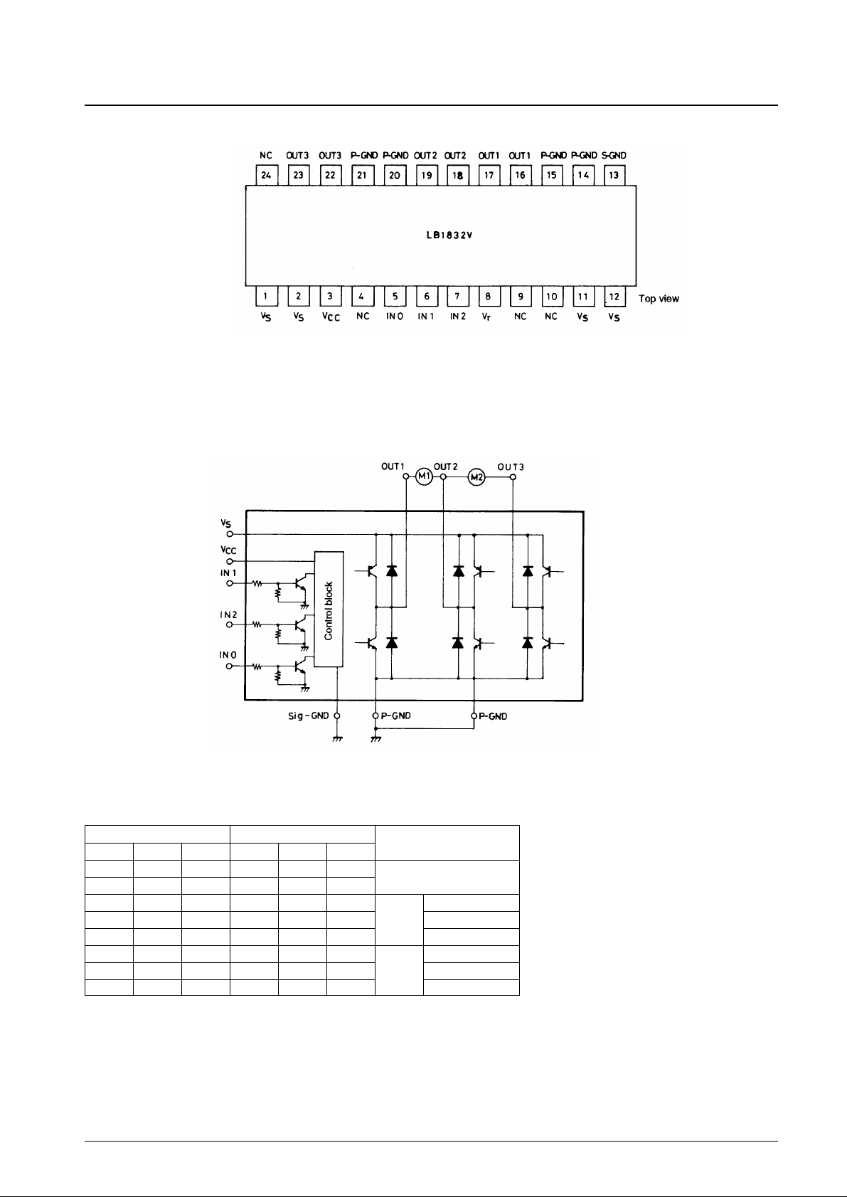
Pin Assignment
Note: 1. VS(motor power supply pins)
Connect either pins 1 and 2 or pins 11 and 12. The wiring resistance falls if all four are connected.
2. P-GND (motor power supply ground pins)
Connect all four of these pins
3. S-GND (Control power supply ground pin)
Connect to the microprocessor ground.
Block Diagram
Note: The two P-GND pins must be connected to a ground as close as possible to the IC.
Truth Table
Note: Blanks are off.
No. 4179-3/7
LB1832V
Input Output
Mode
IN0 IN1 IN2 OUT1 OUT21 OUT3
L L L
Standby
H L L
L H L H L Forward
L L H L H ch1 Reverse
L H H L L Brake
H H L L H Forward
H L H H L ch2 Reverse
H H H L L Brake
 Loading...