

SANYO LB1830M Datasheet

Ordering number: EN3518A
Monolithic Digital IC
LB1830M
Low-Saturation Bidirectional Motor Driver
for Low-Voltage Applications
Overview
The LB1830M is a low-saturation bidirectional motor driver IC
with brake function for use in low-voltage applications. As
both of forward and reverse outputs are regulated, it is
especially suited for use in portable equipment such as VCR,
camera.
Features
.
Wide operating voltage range: 3.0 to 9.0 V
.
Low saturation voltage: 0.2 V at IO= 40 mA (typ)
.
Low current drain at standby mode (0.1 µA or less)
.
Brake function
.
Regulated voltage value (forward/reverse) setting available
by one variable resistor
.
Regulated output/saturation output switching available
.
Built-in spark killer diodes
.
MFP-10S package
Specifications
Package Dimensions
unit: mm
3086A-MFP10S
[LB1830M]
SANYO : MFP10S
Absolute Maximum Ratings atTa=25°C
Parameter Symbol Conditions Ratings Unit
Maximum supply voltage V
Output current Im max 200 mA
Input supply voltage V
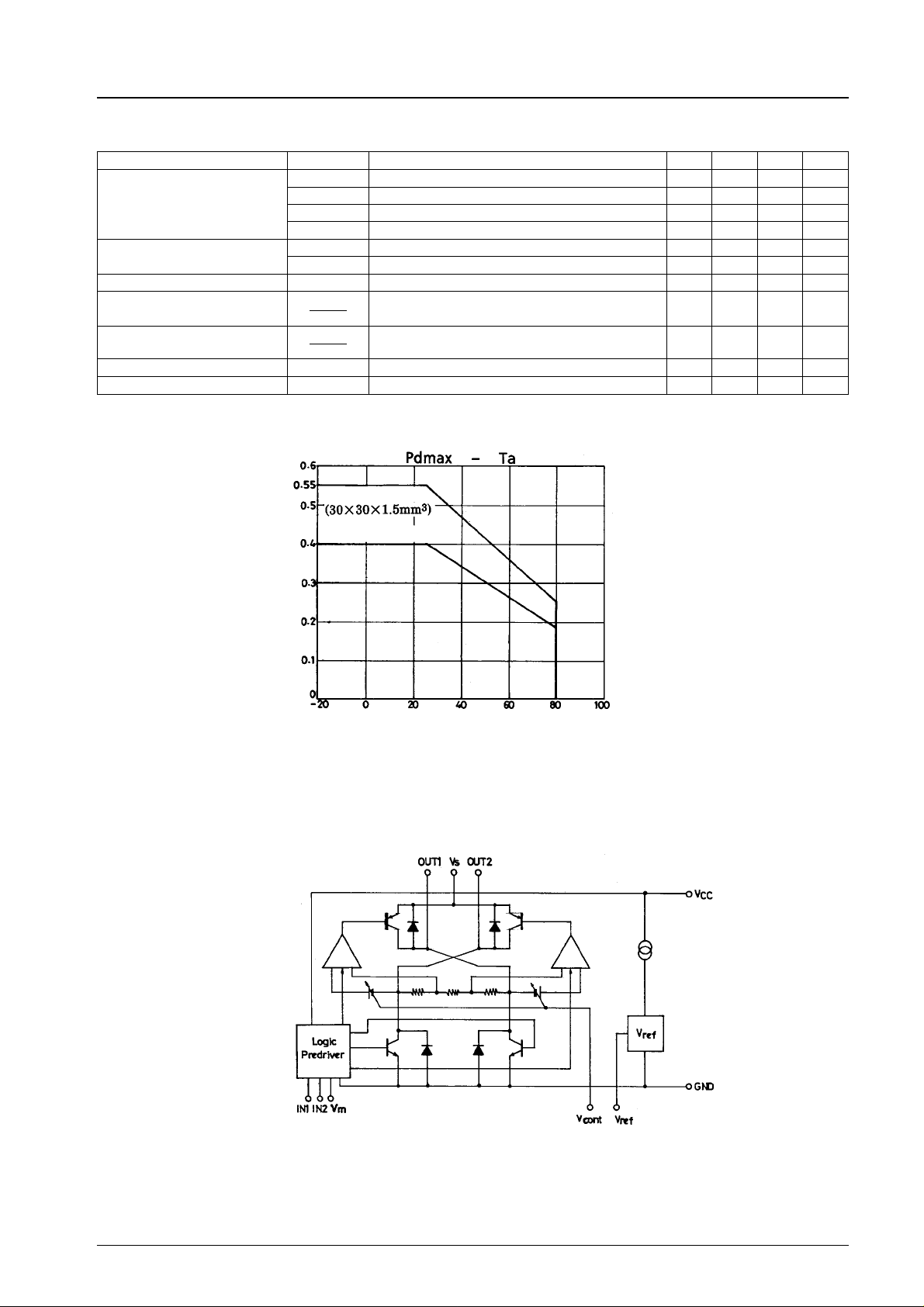
Allowable power dissipation Pd max
Operating temperature Topr –20 to +80
Storage temperature Tstg –40 to +125
max 10.5 V
CC
IN
Independent IC 0.4 W
With specified board (30 × 30 × 1.5 mm
–0.3 to +10 V
3
) 0.55 W
Allowable Operating Ranges atTa=25°C
Parameter Symbol Conditions Ratings Unit
Supply voltage V
Input high level voltage V
Input low level voltage V
Control voltage V
CC
IH
IL
C
3.0 to 9.0 V
2.0 to 9.0 V
–0.3 to +0.3 V
1.0 to 6.0 V
C
°
C
°
SANYO Electric Co.,Ltd. Semiconductor Bussiness Headquarters
TOKYO OFFICE Tokyo Bldg., 1-10, 1 Chome, Ueno, Taito-ku, TOKYO, 110 JAPAN
13097HA (II)/6150TA No.3518-1/3
LB1830M
Electrical Characteristics atTa=25°C, VCC=6V
Parameter Symbol Conditions min typ max Unit
0 IN1=IN2=Vm=0V,VC= Vref at standby mode 0.1 10 µA
I
CC
I
1 Forward/reverse, control, load OPEN 2 3 mA
Current drain
Output saturation voltage
Reference voltage V
Voltage characteristics of
output voltage
Current characteristics of
output voltage
Input current I
Output voltage V
CC
I
2 Forward/reverse, saturation, load OPEN 3 5 mA
CC
I
3 Braking, load OPEN 5 8 mA
CC
V
sat1
V
sat2
ref
∆V
∆V
∆V
∆I
CC
IN
With specified board
IO= 40 mA (upper + lower) 0.2 0.3 V
IO= 80 mA (upper + lower) 0.4 0.6 V
I
= 1 mA 1.85 2.0 2.15 V
Vref
O
VO=5V,VCC=5.5to9V,IO=40mA 80 mV
CC
O
VO=5V,VCC=6V,IO=10to80mA 50 mV
VIN= 5 V 90 150 µA
VC=2V
O
2.3 × V
C
2.5 × VCV
Independent IC
Allowable power dissipation, Pd max − W
Equivalent Circuit Block Diagram
Ambient temperature, Ta −°C
No.3518-2/3
 Loading...