

SANYO LB1825 Datasheet
Overview
The LB1825 is a three-phase brushless motor driver IC
optimal for LBP polygon mirror and magneto-optical disk
spindle motor drive.
Functions and Features
• Three-phase full-wave current control drive
• PLL speed control
• Internal 24-mode clock divisor switching
• Phase lock detector output
• FG/Hall FG selection
• Current limiter circuit
• 7 V stabilized power supply output pin
• Reverse torque braking
• Crystal oscillator circuit
• Internal/external reference frequency selection
• Built-in FG amplifier and FG pulse output
• Forward/reverse rotation switching
• Low power supply voltage protection circuit
• Thermal protection circuit
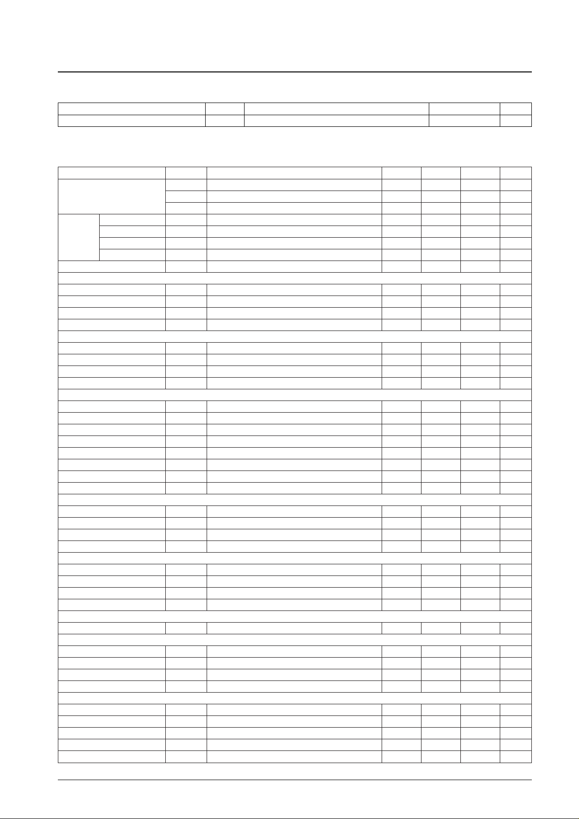
Package Dimensions
unit: mm
3147A-DIP28H
Monolithic Digital IC
Ordering number : EN4845B
83097HA (OT)/N3095HA (OT)/91494TH (OT) No. 4845-1/9
SANYO: DIP28H
[LB1825]
SANYO Electric Co.,Ltd. Semiconductor Bussiness Headquarters
TOKYO OFFICE Tokyo Bldg., 1-10, 1 Chome, Ueno, Taito-ku, TOKYO, 110 JAPAN
Three-Phase Brushless Motor Driver
LB1825
Specifications
Absolute Maximum Ratings at Ta = 25°C
Parameter Symbol Conditions Ratings Unit
Maximum supply voltage V
CC
max 30 V
Maximum output current I
O
max t < 0.1 s 2.0 A
Allowable power dissipation
Pd max1 Independent IC 3 W
Pd max2 With an arbitrarily large heat sink 20 W
Operating temperature Topr –20 to +80 °C
Storage temperature Tstg –55 to +150 °C
Allowable Operating Ranges at Ta = 25°C
Electrical Characteristics at Ta = 25°C, VCC= 24 V
No. 4845-2/9
LB1825
Parameter Symbol Conditions Ratings Unit
Supply voltage V
CC
10 to 28 V
Parameter Symbol Conditions min typ max Unit
I
CC
1 Braking stopped mode 35 47 mA
Current drain I
CC
2 FG
OUT
1 stopped mode 35 47 mA
I
CC
3 External clock, braking stopped mode 28 40 mA
Upper transistor (1) V
O
(sat)1 IO= 1.0 A 1.0 1.6 V
Upper transistor (2) V
O
(sat)2 IO= 1.5 A 1.25 2.1 V
Lower transistor (1) V
O
(sat)1 IO= 1.0 A 0.6 1.0 V
Lower transistor (2) V
O
(sat)2 IO= 1.5 A 0.9 1.6 V
Output leakage current I
O LEAK
100 µA
[Fixed voltage block]
Output voltage V
REGIREG
= 20 mA 6.3 7.0 7.8 V
Output current I
REG
20 mA
Load variation ∆V
REGIREG
= 0 to 20 mA 0.25 V
Temperature coefficient
αV
REG
Design target value –2.0 mV/°C
[Hall input block]
Input bias current I
B
(HA) 1 4 µA
Common-mode input range 1.5 V
CC
– 1.8 V
Input sensitivity DV
H
20 mV
Input offset voltage V
IOH
20 mV
[Drive block]
Dead zone width V
DZ
50 200 mV
Output idling voltage V
ID
6 mV
Forward gain G
DF
+
0.4 0.5 0.6
Reverse gain G
DF
–
–0.6 –0.5 –0.4
Accelerate command voltage V
STA
6.0 6.3 V
Decelerate command voltage V
STO
0.8 1.5 V
Forward limiter voltage V
L
+
Rf= 1.8 Ω 0.45 0.53 0.61 V
Reverse limiter voltage V
L
–
Rf= 1.8 Ω 0.45 0.53 0.61 V
[Phase comparator block]
Output high level voltage V
PDH
No external load V
REG
– 0.4 V
Output low level voltage V
PDL
No external load 0.4 V
Output source current I
PD
+
0.4 mA
Output sink current I
PD
–
2.5 mA
[Error amplifier block]
Input bias current I
B
(ER) 1 µA
Input offset voltage V
IO
(ER) –10 +10 mV
Output high level voltage V
ERH
No external load 5.5 V
Output low level voltage V
ERL
No external load 1.0 V
[Lock detector block]
Output saturation voltage V
LD
(sat) ILD= 10 mA 0.4 V
[FG amplifier block]
Input bias current I
B
(FG) 1 µA
Input offset voltage V
IO
(FG) –10 +10 mV
Output high level voltage V
FGH
No external load 5.0 V
Output low level voltage V
FGL
No external load 2.0 V
[FG Schmitt block]
Input operating level V
IS
FG
OUT
1 generation signal 160 mVp-p
Input hysteresis (high → low) V
SHL
External clock, braking stopped mode 0 mV
Input hysteresis (low → high) V
SLH
External clock, braking stopped mode 36 mV
Hysteresis V
FGS
18 36 60 mV
Output saturation voltage V
FG2
(sat) I
FG2
= 10 mA 0.4 V
Continued on next page.
Output
saturation
voltage
Continued from preceding page.
No. 4845-3/9
LB1825
Parameter Symbol Conditions min typ max Unit
[FG switching setting]
Single Hall FG operating level V
FGIH
FGINpin voltage V
REG
– 0.1 V
REG
V
Triple Hall FG operating level V
FGIL
FGINpin voltage 0 0.1 V
[Stop mode setting]
FG
OUT
1 low level voltage V
FG1
L 0.4 V
FG
OUT
1 low level current I
FG1
L FG
OUT
1 pin voltage = 0 V 0.6 2.4 mA
[Current limiter]
Reference voltage V
CS
R = 47 kΩ 0.51 0.58 0.65 V
External supply range V
CS
(EX) 0.7 3.0 V
Offset voltage V
CSO
R = 47 kΩ, Rf= 1.8 Ω 25 50 90 mV
[Signal block]
Internal oscillator frequency f
OSC
Crystal oscillator mode 1 12 MHz
External input frequency f
REF
External clock mode 30 5000 Hz
Low level pin voltage V
OSCL
4.0 4.5 5.0 V
High level pin current I
OSCH
0.3 0.5 0.75 mA
[Divisor switching]
Input high level voltage V
N1 to 3
H 4.2 V
REG
V
Input middle level voltage V
N1 to 3
M 2.1 2.9 V
Input low level voltage V
N1 to 3
L 0 0.8 V
[F/R switching]
Input high level voltage V
FRH
2.4 V
REG
V
Input low level voltage V
FRL
0 1.5 V
High level input current I
FRH
F/R pin voltage = V
REG
0.22 mA
[S/B switching]
Input high level voltage V
SBH
2.4 V
REG
V
Input low level voltage V
SBL
1.5 V
Hysteresis (high → low) DV
SB
0.15 0.25 0.35 V
[Stop detection]
S
CT
1 FG mode 32
Count setting S
CT
2 Triple Hall FG mode 8
S
CT
3 Single Hall FG mode 2
[Undervoltage protection]
Operating voltage V
SD
8.4 8.8 9.2 V
Hysteresis DV
SD
0.2 0.4 0.6 V
[Thermal protection]
Operating temperature T
SD
Design target value 150 180 °C
Recovery temperature T
SDR
Design target value 140 °C
[Pin leakage currents]
LD pin I
LD (LEAK)
Pin voltage = 30 V 10 µA
FG
OUT
2 pin I
FG2 (LEAK)
Pin voltage = 30 V 10 µA
[GND pin-heat sink]
Resistance Design target value. 30 Ω
 Loading...