

Page 1
Ordering number : ENN5805
LB1817W
Monolithic Digital IC
LB1817W
FDD Spindle Motor Driver
Overview
The LB1817W is a spindle motor driver for low-profile
floppy disk drives.
Functions and Features
• Three-phase full-wave linear drive
(with external PNP transistor)
• Low saturation voltage
• Built-in digital speed control
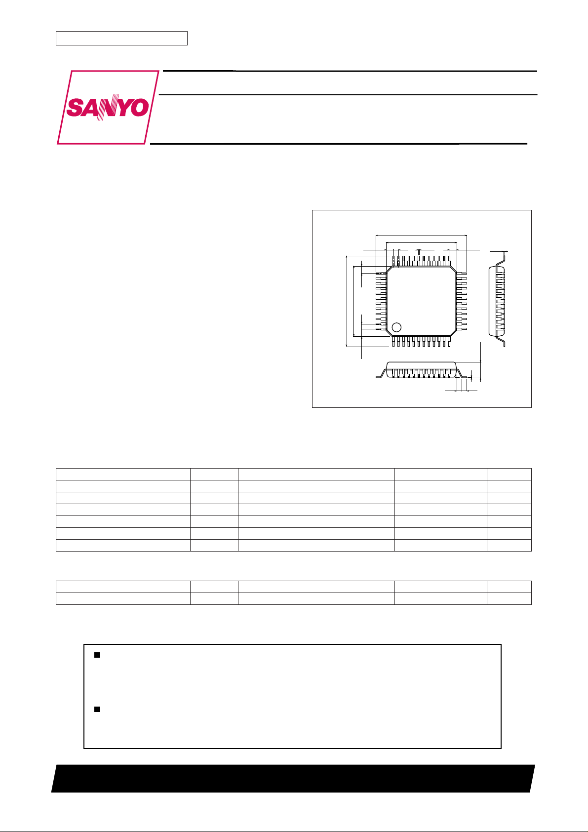
Package Dimensions
unit: mm
3163A-SQFP48
[LB1817W]
9.0
7.0
0.180.75 0.5
36
37
0.75
7.0
9.0
0.75
25
0.15
24
• Start/stop circuit (Low active)
• Switchable rotation speed
• Current limiter circuit
• Built-in index processing circuit
• Index timing adjustable by VR
• AGC circuit
• Thermal protection circuit
0.5
0.75
48
112
13
0.1
0.5
0.5
SANYO : SQFP48
1.7max
Specifications
Absolute Maximum Ratings at Ta = 25°C
Parameter Symbol Conditions Ratings Unit
Maximum supply voltage VCC max 7.0 V
Maximum output current ICC max1 t ≤ 0.5s 1.5 A
Maximum constant output current IO max2 1.0 A
Allowable power dissipation Pd max1 IC only 0.45 W
Operating temperature Topr –20 to +80 °C
Storage temperature Tstg –40 to +150 °C
Allowable Operating Ranges at Ta = 25°C
Parameter Symbol Conditions Ratings Unit
Power supply voltage V
Any and all SANYO products described or contained herein do not have specifications that can handle
applications that require extremely high levels of reliability, such as life-support systems, aircraft's
control systems, or other applications whose failure can be reasonably expected to result in serious
physical and/or material damage. Consult with your SANYO representative nearest you before using
any SANYO products described or contained herein in such applications.
SANYO assumes no responsibility for equipment failures that result from using products at values that
exceed, even momentarily, rated values (such as maximum ratings, operating condition ranges, or other
parameters) listed in products specifications of any and all SANYO products described or contained
herein.
CC
SANYO Electric Co.,Ltd. Semiconductor Company
TOKYO OFFICE Tokyo Bldg., 1-10, 1 Chome, Ueno, Taito-ku, TOKYO, 110-8534 JAPAN
4.2 to 6.5 V
73099RM(KI)
No. 5805-1/9
Page 2
LB1817W
Electrical Characteristics at Ta = 25°C, VCC = 5V
Parameter Symbol Conditions
Current drain I
CCO
I
S/S = 5V (Standby) 70 100 µA
S/S = 0V (Normal) 25 35 mA
CC
MS1 bias current IMS1VMS1 = 5V 180 270 µA
MS1 Low input voltage VMS1L 0.0 0.8 V
MS1 High input voltage VMS1H 2 V
MS2 bias current IMS2VMS2 = 5V 90 135 µA
MS2 Low input voltage VMS2L 0.0 0.8 V
MS2 High input voltage VMS2H 2 V
MS3 bias current IMS3VMS3 = 5V 90 135 µA
MS3 Low input voltage VMS3L 0.0 0.8 V
MS3 High input voltage VMS3H 2 V
S/S bias current I
S/S Low voltage V
S/S High voltage V
Hall amplifier input bias current I
S/S
S/SL
S/SH
HB
Common mode input voltage range Vh 2.0
Differential input voltage range Vdif 50 200 mVp-p
Input offset voltage Vho * ±10 mV
Hall bias output voltage V
Leakage current V
IH = 5 mA 0.5 0.8 1.1 V
H
S/S = 5V ±10 µA
HL
Output saturation voltage V(sat) IO = 0.8A 0.45 0.64 V
Output leakage current I
Current limiter I
Control amplifier voltage gain G
Voltage gain phase differential ∆G
V/I conversion source current I
V/I conversion sink current I
V/I conversion current ratio I+/I
DSC buffer input current I
FG amplifier input voltage V
FG amplifier voltage gain G
FG amplifier input offset V
FG amplifier internal reference voltage
V
OL
lim
DSC
FG
FG
FGO
FGB
C
C
+
–
–
RF = 3 kΩ, R
= 100Ω 6.3 7.5 8.7 mA
OUT
fFG = 300 Hz 2 20 mVp-p
Open loop* 60 dB
* ±10 mV
FG Schmitt hysteresis width ∆Vsh1 High –> Low* 25 mV
∆Vsh2 Low –> High* 25 mV
Speed discriminator count N 1390/2
Discriminator operating frequency F
Oscillator frequency F
OSC
Oscillator frequency tolerance ∆F
Index output Low voltage V
Index output leakage current I
Index amplifier common mode input voltage range
Index amplifier differential input voltage range
Index amplifier hysteresis set current I
V
HYS
Timing adjustment at High level V
Timing adjustment at Low level V
Timing adjustment ratio T
Reference voltage V
Thermal protection operating temperature
REF
V
REF
TSD * 150 180 °C
* 1.1 MHz
D
* 1.1 MHz
OSC
IDLIO
IDL
V
I
DIF
TH
TL
HL
= 2 mA 0.4 V
Hysteresis width < 25 mA 25 100 mV
MS1 = L 1.15 1.26 1.35 V
MS1 = L 0.40 0.52 0.60 V
V
(MS1 = L) / VTH (MS1 = H) 1.148
TH
1 2.20 2.50 2.80 V
2 1.85 2.15 2.45 V
Hysteresis width ∆TSD * 10 °C
Note: Items shown to be “*” are not measured.
Ratings
min typ max
CC
CC
CC
20 µA
0.0 0.8 V
2VCCV
15 µA
VCC–0.7
1mA
–7.5 –5.5 –3.5 dB
±1dB
19 28 37 µA
–19 –28 –37 µA
0.8 1.0 1.2
1 µA
2.2 2.5 2.8 V
±0.2 %
±10 µA
0.2
VCC–0.7
2.9 4.2 5.5 µA
Unit
V
V
V
V
V
No. 5805-2/9
Page 3
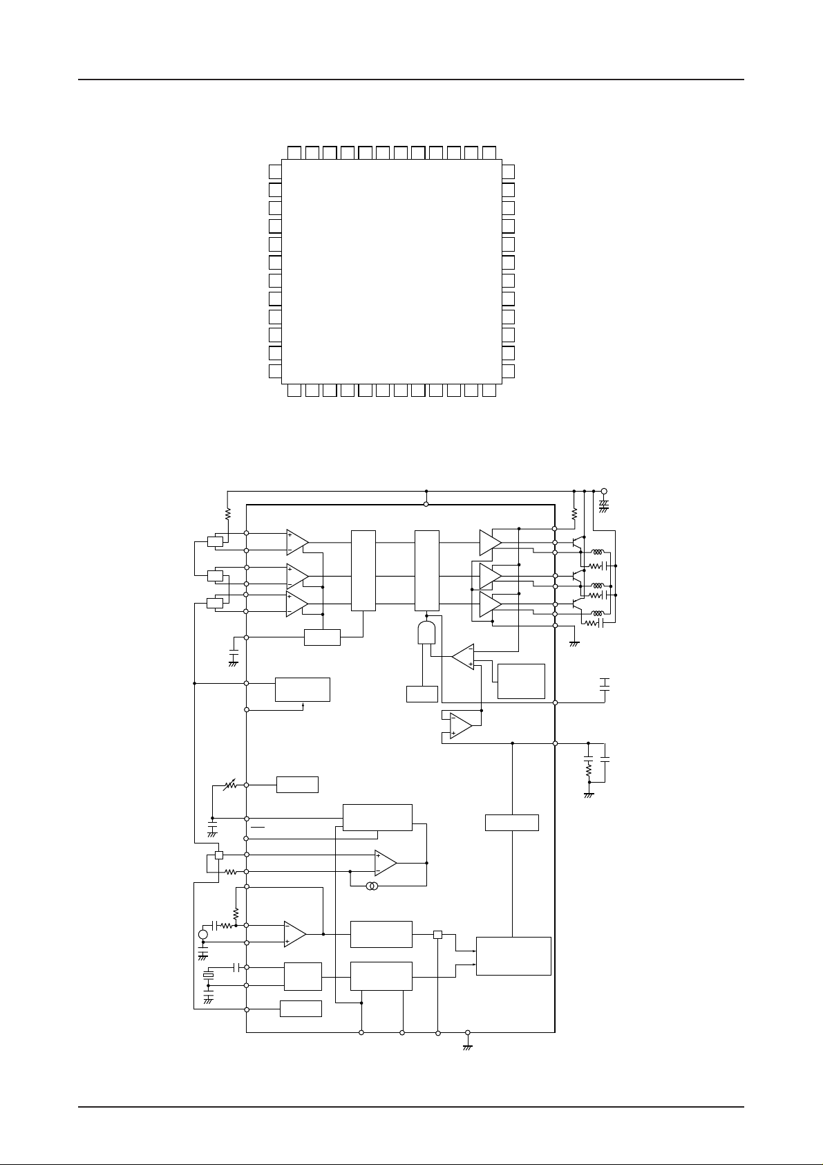
LB1817W
Pin Assignment
Block Diagram
HU
HV
HW
NC
VIN2
VIN1
WIN2
WIN1
HB
V
AGC
DSC
CT
NC
NC
UIN1
U
V
V
W
W
AGC
CC
37
38
39
40
41
42
43
44
45
46
47
48
2
IN
1
IN
2
IN
1
IN
2
IN
UIN134UIN233WPB32W
36NC35
1
2
3
1
NC
REF
V
Hall amplifier
U
V
W
AGC
OUT
LB1817W
4
5NC6SG7
2
I/D
REF
V
Matrix
31NC30
OUT
VPB29V
UPB27U
28
10
MS38MS29MS1
V
CC
Current control
OUT
OUT
G
F
NC
26
25
24
23
22
21
20
19
18
17
16
15
14
13
11
12
–
I
NC
S/S
Output amplifier
U
V
W
Control
amplifier
NC
FG
FG
PG
Rf
NC
FC
X2
X1
+
I
NC
NC
–
+
Top view
R
F
U
PB
U
OUT
V
PB
V
OUT
W
PB
W
OUT
PGND
LB1817W
V
CC
750kΩ
12kΩ
N
0.22µF
1MHz
HB
S/S
1
V
REF
CT
I/D
+
I
–
I
FG OUT
–
FG
+
FG
X2
X1
V
2
REF
Hall bias
V
1
REF
FG amplifier
V
2
REF
TSD
Buffer amplifier
Timing
adjustment
5µA
Schmitt
comparator
1 / NOSC
MS1
(1:1.2)
H:1.2
L:1
H:360rpm
()
L:300rpm
(1:2)
H:2
L:1
MS3MS2
Current
limiter
V
LIM
V/I
Speed
discriminator
(1390/2 count)
SGND
FC
DSC
V
CC
No. 5805-3/9
Page 4

Pin Descriptions
Pin number
1, 5
12, 13
14, 19
24, 25
31, 36
37, 47
48
2
3
Pin name
NC
V
REF
V
REF
1
2
Pin voltage
2.5V typ
2.15V typ
100Ω
LB1817W
Equivalent circuit
Pin function
• Pins not used
•V
1 pin.
V
CC
REF
Used as power supply for external CR
serving for index timing adjustment.
2
•V
2 pin.
V
CC
REF
Used as bias pin for external index
sensor.
3
4
I/D
V
CC
• Index pulse output pin.
4
6
SG
• Signal ground pin.
Connect to ground together with pin 21.
7
MS3
H: 2.0V min
L: 0.8V max
7
50kΩ
50kΩ
8
MS2
H: 2.0V min
L: 0.8V max
8
50kΩ
50kΩ
• FG switching pin.
V
CC
High: FG set to through
Low: FG set to 1-stage division
• CLK switching pin.
V
CC
High: Clock set to through
Low: Clock set to 1-stage division
Continued on next page
No. 5805-4/9
Page 5

Continued from preceding page
Pin number
9
Pin name
MS1
Pin voltage
H: 2.0V min
L: 0.8V max
LB1817W
Equivalent circuit Pin function
• Rotation speed switching pin.
V
CC
9
50kΩ
50kΩ
50kΩ
50kΩ
High: 360 rpm
Low: 300 rpm
For details, see rotation speed switching
table.
10
11
15
16
S/S
I
I
X1
–
+
H: 2.0V min
L: 0.8V max
11
16
200Ω
I
1
200Ω200Ω
400Ω
200Ω 200Ω
10
• Start/stop switching pin.
V
CC
Low: active
• External index – input pin.
V
CC
• External index + input pin.
When I– pin is High, constant current I1
flows. When pin is Low, constant current
15
I1 is cut off.
Resistor externally connected to I– pin
determines hysteresis width.
• Reference clock generator pin.
V
CC
17
18
X2
FC
17
200Ω
18
V
CC
• Frequency characteristics compensation
pin.
T o prevent current control loop oscillation,
insert a capacitor between this pin and
VCC.
Continued on next page
No. 5805-5/9
Page 6

Continued from preceding page
Pin number
20
Pin name
RF
Pin voltage
LB1817W
Equivalent circuit Pin function
• Output current detection pin.
To detect output current as a voltage,
insert a resistor Rf between this pin and
VCC. The voltage is used for the current
limiter. The detection level is about 1/50
of the output current.
21
22
23
26
PG
FG
FG
FGout
• Output transistor ground pin.
Connect to ground together with pin 6.
+
–
2.5V typ
12kΩ
12kΩ
100Ω
200Ω
200Ω
1kΩ200Ω
39Ω
39Ω
200Ω
V
CC
• FG amplifier + pin
V
CC
• FG amplifier – pin
2322
• FG amplifier output pin.
V
CC
26
27
28
29
30
32
33
34
35
38
39
40
41
U
OUT
U
V
OUT
V
W
OUT
W
UIN2
UIN1
VIN2
VIN1
WIN2
WIN1
PB
PB
PB
V
CC
35
200Ω 200Ω
39
41
28
30
33
21
• U phase output pin.
• U phase external PNP transistor base
27
29
32
connection.
• V phase output pin.
• V phase external PNP transistor base
connection.
• W phase output pin.
• W phase external PNP transistor base
connection.
• U phase Hall input pin.
V
CC
Logic High means UIN1 > UIN2.
• V phase Hall input pin.
Logic High means VIN1 > VIN2.
• W phase Hall input pin.
34
Logic High means WIN1 > WIN2.
38
40
Continued on next page
No. 5805-6/9
Page 7

Continued from preceding page
Pin number
42
Pin name
HB
Pin voltage
LB1817W
Equivalent circuit Pin function
V
CC
• Hall bias negative-side pin.
In stop mode, the pin is open and Hall
42
bias is cut off.
43
44
45
46
V
CC
AGC
DSC
CT
46
45
100Ω
44
200Ω
200Ω
100Ω
• Power supply pin.
The voltage supplied to this pin must be
stabilized to prevent ripple noise or other
noises from inputting to this pin.
• AGC pin.
V
CC
Controls the Hall amplifier gain according
to Hall input amplitude.
An external capacitor is used.
• Speed discriminator pin.
V
CC
• Timing adjustment pin.
V
CC
External CR for time constant circuit is
connected here.
No. 5805-7/9
Page 8

LB1817W
Truth Table
Source –> Sink
1 V phase –> W phase H H L
2 V phase –> U phase L H L
3 W phase –> U phase L H H
4 W phase –> V phase L L H
5 U phase –> V phase H L H
6 U phase –> W phase H L L
Hall input pin High means UIN1 > UIN2
VIN1 > VIN2
WIN1 > WIN2
UVW
Rotation Speed Select Table
f
MS1 HLHLHLHL
MS2 H L H L
MS3 H L L H
fFG [Hz] 720 600 720 600 1440 1200 360 300
OSC
= 1 MHz
Hall input
Pd max – Ta
0.6
0.5
0.4
0.3
0.2
0.1
Allowable power dissipation, Pd max – W
0
–20 0 20 40 60 80 100
Ambient temperature, Ta – °C
0.28
No. 5805-8/9
Page 9

Index and Timing Chart
LB1817W
HYS
1.25V ; MS1 = L
1.08V ; MS1 = H
+
I
2.5V
CT
Falling edge
I/D
T
.
V
1 = 2.5V
REF
.
R
.
T = 0.693CR
.
.
T = 0.578CR
.
...
...
(Open-collector)
MS1 = L
MS1 = H
Output
CT
C
Specifications of any and all SANYO products described or contained herein stipulate the performance,
characteristics, and functions of the described products in the independent state, and are not guarantees
of the performance, characteristics, and functions of the described products as mounted in the customer's
products or equipment. To verify symptoms and states that cannot be evaluated in an independent device,
the customer should always evaluate and test devices mounted in the customer's products or equipment.
SANYO Electric Co., Ltd. strives to supply high-quality high-reliability products. However, any and all
semiconductor products fail with some probability. It is possible that these probabilistic failures could
give rise to accidents or events that could endanger human lives, that could give rise to smoke or fire,
or that could cause damage to other property. When designing equipment, adopt safety measures so
that these kinds of accidents or events cannot occur. Such measures include but are not limited to protective
circuits and error prevention circuits for safe design, redundant design, and structural design.
In the event that any or all SANYO products(including technical data,services) described or
contained herein are controlled under any of applicable local export control laws and regulations,
such products must not be exported without obtaining the export license from the authorities
concerned in accordance with the above law.
No part of this publication may be reproduced or transmitted in any form or by any means, electronic or
mechanical, including photocopying and recording, or any information storage or retrieval system,
or otherwise, without the prior written permission of SANYO Electric Co. , Ltd.
Any and all information described or contained herein are subject to change without notice due to
product/technology improvement, etc. When designing equipment, refer to the "Delivery Specification"
for the SANYO product that you intend to use.
Information (including circuit diagrams and circuit parameters) herein is for example only ; it is not
guaranteed for volume production. SANYO believes information herein is accurate and reliable, but
no guarantees are made or implied regarding its use or any infringements of intellectual property rights
or other rights of third parties.
This catalog provides information as of July, 1999. Specifications and information herein are subject to change
without notice.
No. 5805-9/9
PS
 Loading...