

Page 1
Ordering number : EN4355
73098HA (OT)/20593TS A8-9155 No. 4355-1/9
Overview
The LB1817M is the ideal IC for applications requiring a
5 V, low-profile FDD spindle motor driver.
Functions and Features
• Three phase total wave linear driver (external PNP)
• Low saturation voltage
• On-chip digital speed control
• Start/stop circuit (“L” level active)
• Rotation speed switching
• Current limiter circuit
• On-chip index processing circuit
• Index timing supports adjustments using VR
• AGC circuit
• Temperature protection circuit
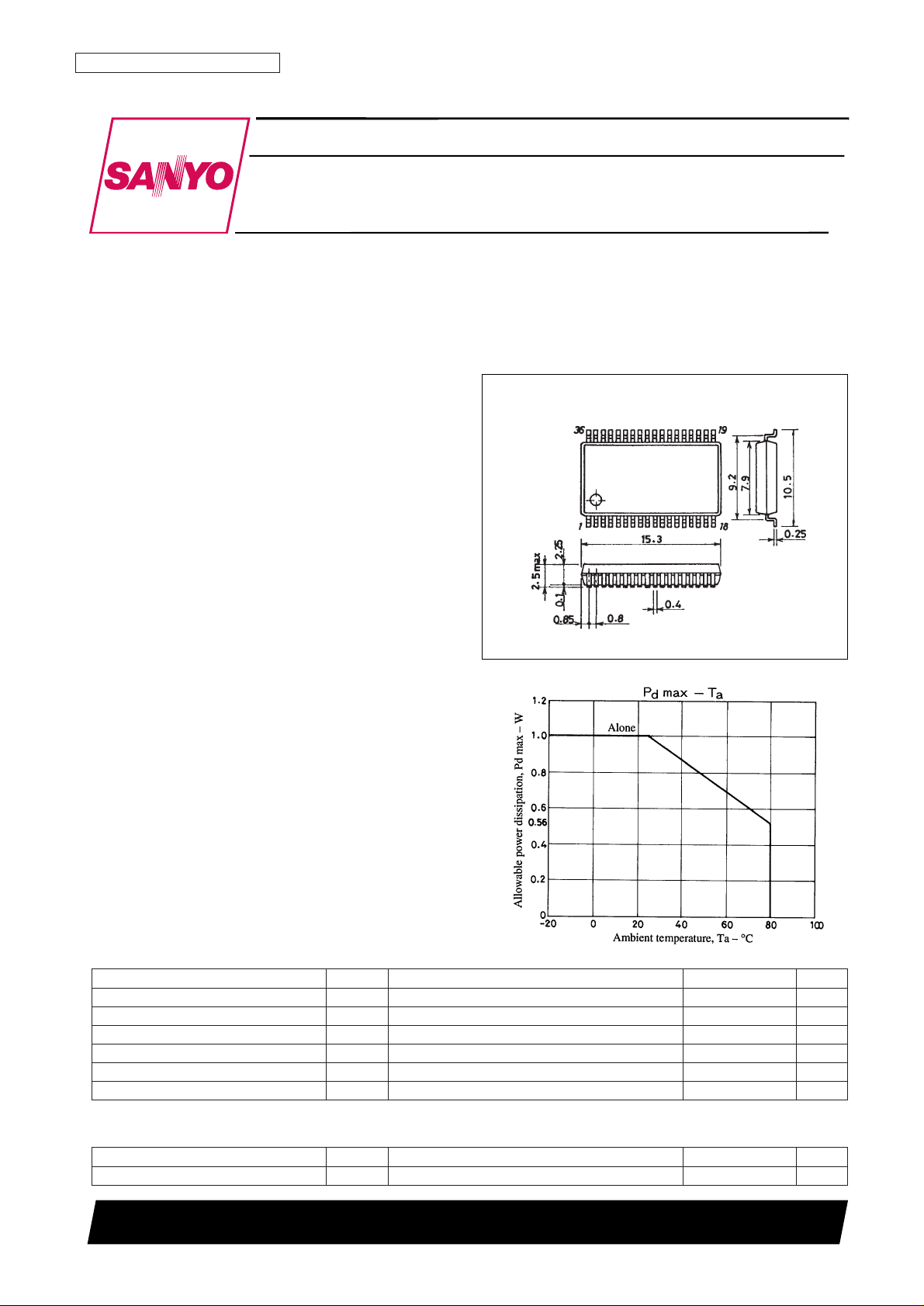
Package Dimensions
unit: mm
3129-MFP36S
SANYO: MFP36S
[LB1817M]
LB1817M
SANYO Electric Co.,Ltd. Semiconductor Bussiness Headquarters
TOKYO OFFICE Tokyo Bldg., 1-10, 1 Chome, Ueno, Taito-ku, TOKYO, 110-8534 JAPAN
FDD Spindle Motor Driver
Monolithic Digital IC
Specifications
Absolute Maximum Ratings at Ta = 25°C
Allowable Operating Conditions at Ta = 25°C
Parameter Symbol Conditions Ratings Unit
Supply voltage V
CC
4.2 to 6.5 V
Parameter Symbol Conditions Ratings Unit
Maximum supply voltage V
CC
max 7.0 V
Maximum output current I
CC
max1 t≤0.5 1.5 A
Steady maximum output current I
O
max2 1.0 A
Allowable power dissipation Pd max Independent IC 1 W
Operating temperature Topr –20 to +80 °C
Storage temperature range Tstg –40 to +150 °C
Page 2
LB1817M
No. 4355-2/9
Electrical Characteristics at Ta = 25°C, VCC= 5V
Note: Marked values (*) are guaranteed by the design itself and therefore do not require measurement.
Ratings
Parameter Symbol Conditions
min typ max
Unit Note
Current drain
I
CCO
S/S = 5V (Standby) 70 100 µA
I
CC
S/S = 0V (Steady) 25 35 mA
MS1 bias current I
MS1
V
MS1
= 5V 180 270 µA
MS1 “L” level input voltage V
MS1L
0 0.8 V
MS1 “H” level input voltage V
MS1H
2.0 V
CC
V
MS2 bias current I
MS2
V
MS2
= 5V 90 135 µA
MS2 “L” level input voltage V
MS2L
0 0.8 V
MS2 “H” level input voltage V
MS2H
2.0 V
CC
V
MS3 bias current I
MS3
V
MS3
= 5V 90 135 µA
MS3 “L” level input voltage V
MS3L
0 0.8 V
MS3 “H” level input voltage V
MS3H
2.0 V
CC
V
S/S bias current I
S/S
20 µA
S/S “L” level voltage V
S/SL
0 0.8 V
S/S “H” level voltage V
S/SH
2.0 V
CC
V
Hall-effect bias amplifier input current I
HB
15 µA
In-phase input voltage range Vh 2.0 VCC– 0.7 V
Differential input voltage range Vdif 50 200 mVp-p
Input offset voltage Vho ±10 mV *
Hall-effect output voltage V
H
IH= 5mA 0.5 0.8 1.1 V
Leak current I
HL
S/S = 5V ±10 µA
Output saturation voltage Vsat IO= 0.8A 0.45 0.64 V
Output leak current I
OL
1.0 mA
Current limiter I
lim
RF= 3kΩ, ROUT = 100Ω 6.3 7.5 8.7 mA
Control amplifier voltage gain G
C
–7.5 –5.5 –3.5 dB
Voltage gain phase differential ▲▲G
C
±1 dB
V/I conversion source current I
+
19 28 37 µA
V/I conversion sink current I
–
–19 –28 –37 µA
V/I conversion current ratio I+/I
–
0.8 1.0 1.2
DSC buffer input current I
DSC
1.0 µA
FG amplifier input voltage V
FG
fFG= 300Hz 2 20 mVp-p
FG amplifier voltage gain G
FG
Open loop 60 dB *
FG amplifier input offset V
FGO
±10 mV *
FG amplifier internal reference voltage V
FGB
2.2 2.5 2.8 V
FG schmitt hysteresis width
▲▲Vsh1 “H”
→ “L” 25 mV *
▲▲Vsh2 “L” → “H” 25 mV *
Speed disk recount number N 1390/2
Disk operation frequency F
D
1.1 MHz *
Oscillation range F
OSC
1.1 MHz *
Oscillation frequency error ▲▲F
OSC
±0.2 %
Index output “L” level voltage V
IDL
IO= 2mA 0.4 V
Index output leak current I
IDL
±10 µA
Index amplifier in-phase input voltage range V
I
0.2 VCC–0.7 V
Index amplifier differential input voltage range V
DIF
Hysteresis width<25mA 25 100 mV
Index amplifier hysteresis setting current I
HYS
2.9 4.2 5.5 µA
Timing adjustment “H” level V
TH
MS1 = L 1.15 1.26 1.35 V
Timing adjustment “L” level V
TL
MS1 = L 0.4 0.52 0.6 V
Timing adjustment ratio T
HL
VTH(MS1 = L)/VTH(MS1 = H)
1.148
Reference voltage
V
REF1
2.20 2.50 2.80 V
V
REF2
1.85 2.15 2.45 V
Excessive heat protected operating temperature TSD 150 180 °C *
Hysteresis width ▲▲TSD 10 °C *
Page 3
LB1817M
No. 4355-3/9
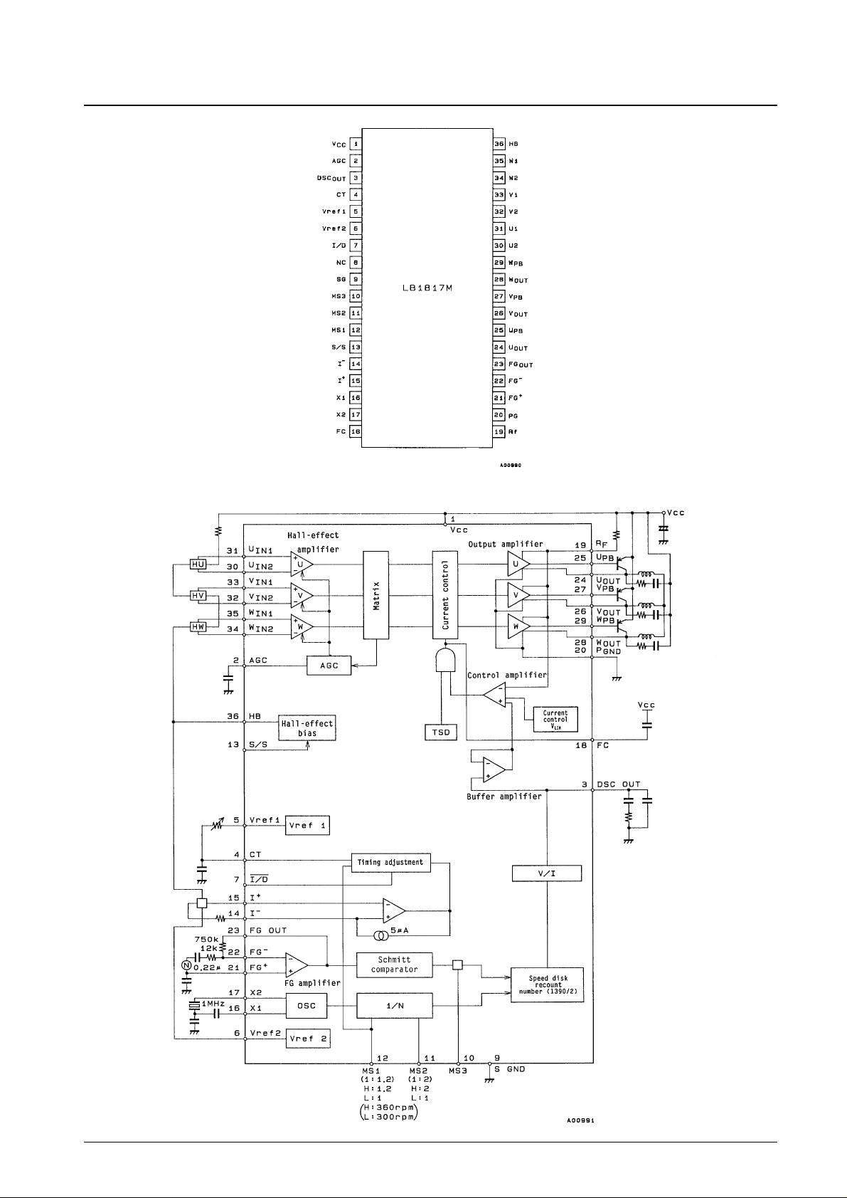
Pin Assignment
Block Diagram
[Top view]
Unit (resistance: Ω, capacitance: F)
Page 4

LB1817M
No. 4355-4/9
Pin Description
Pin No. Symbol Pin voltage Equivalent circuit Pin description
1 V
CC
• Power supply voltage pin.
Voltage must be stable and free of ripple
noise interference.
2 AGC • AGC pin.
Controls hall-effect amplifier gain in
response to hall-effect input frequency.
External capacitor installation.
3 DSC out • Speed discriminator pin.
4 CT • Timing adjustment pin.
External CR for delay time constant
connected.
5 Vref1 2.5V typ • Vref1 pin.
Used as external CR power supply for
index timing adjustment applications.
6 Vref2 2.15V typ • Vref2 pin.
Used for sensor bias for external index
applications.
Continued on next page.
Unit (resistance: Ω)
Page 5

LB1817M
No. 4355-5/9
Continued from preceding page.
Pin No. Symbol Pin voltage Equivalent circuit Pin description
7 I/D • Index pulse output pin.
8 NC • No connection.
9 GND • Ground pin for signal system.
Grounded as with pin 20.
10 MS3 H: 2.0V min • FG changeover pin.
L: 0.8V max When operating at an “H” level, FG sets to
a through state. An “L” level results in 1step division of FG.
11 MS2 H: 2.0V min • CLK changeover pin.
L: 0.8V max When operating at an “H” level, CLK sets
to a through state. An “L” level results in
1-step division of CLK.
12 MS1 H: 2.0V min • Rotation speed changeover pin.
L: 0.8V max An “H” level sets rotation speed to 360
rpm.
An “L” level sets rotation speed to 300
rpm.
For more details, refer to the rotation
speed changeover table.
13 S/S H: 2.0V min • Start/stop changeover pin.
L: 0.8V max “L” level active.
Unit (resistance: Ω)
Continued on next page.
Page 6

LB1817M
No. 4355-6/9
Continued from preceding page.
Pin No. Symbol Pin voltage Equivalent circuit Pin description
14 I
–
• External index negative input pin.
• External index positive input pin.
15 I
+
When the I–pin is at an “H” level, I1
operates with the fixed current; at an “L”
level, I1 does not flow.
Hysteresis width is determined by the
resistor attached externally to the I–pin.
16 X1 • Reference clock generating pin.
17 X2
18 FC • Frequency characteristics revision pin
By installing a capacitor between this pin
and VCC, close-loop oscillation for the
current control system halts.
19 RF • Output current detection pin.
By installing an Rfresistor between this
pin and VCC, output current is detected as
voltage. Voltage detection at this pin
activates the current limiter.
Detection level is approximately 1/50 of
output current.
20 PGND • Output transistor grounding pin.
Grounded as with pin 9.
Continued on next page.
Unit (resistance: Ω)
Page 7

LB1817M
No. 4355-7/9
Continued from preceding page.
Pin No. Symbol Pin voltage Equivalent circuit Pin description
21 FG
+
2.5V typ • FG amplifier positive pin.
• FG amplifier negative pin.
22 FG
–
23 FG out • FG amplifier output pin.
24 U
OUT
• U-phase output pin.
25 U
PB
• Base connection pin for U-phase external
PNP.26 V
OUT
• V-phase output pin.27 V
PB
• Base connection pin for V-phase external
PNP.
28 W
OUT
• W-phase output pin.
29 W
PB
• Base connection pin for W-phase external
PNP.
30 UIN2 • U-phase hall-effect input pin.
31 UIN1 U
IN1
> U
IN2
is established when logic is at
an “H” level.32 VIN2
• V-phase hall-effect input pin.33 VIN1
V
IN1
> V
IN2
is established when logic is at
an “H” level.
34 WIN2
• W-phase hall-effect input pin.
35 WIN1
W
IN1
> W
IN2
is established when logic is at
an “H” level.
36 HB • Hall-effect bias applied to minus-side pin.
When stopped, switches open and halleffect bias severs.
Unit (resistance: Ω)
Page 8

LB1817M
No. 4355-8/9
Truth Table
Source → Sink
Hall-Effect Input
U V W
1 V-phase → W-phase H H L
2 V-phase → U-phase L H L
3 W-phase → U-phase L H H
4 W-phase → V-phase L L H
5 U-phase → V-phase H L H
6 U-phase → W-phase H L L
When an “H” level exists for hall-effect input,
U
IN1
> U
IN2
V
IN1
> V
IN2
W
IN1
> W
IN2
Rotation Speed Changeover Table
f
OSC
= 1MHz
MS1 H L H L H L H L
MS2 H L H L
MS3 H L L H
f
FG
[Hz] 720 600 720 600 1440 1200 360 300
Index and Timing Chart
Page 9

PS No. 4355-9/9
LB1817M
This catalog provides information as of July, 1998. Specifications and information herein are subject to change
without notice.
■ No products described or contained herein are intended for use in surgical implants, life-support systems, aerospace
equipment, nuclear power control systems, vehicles, disaster/crime-prevention equipment and the like, the failure of
which may directly or indirectly cause injury, death or property loss.
■ Anyone purchasing any products described or contained herein for an above-mentioned use shall:
➀ Accept full responsibility and indemnify and defend SANYO ELECTRIC CO., LTD., its affiliates, subsidiaries and
distributors and all their officers and employees, jointly and severally, against any and all claims and litigation and all
damages, cost and expenses associated with such use:
➁ Not impose any responsibility for any fault or negligence which may be cited in any such claim or litigation on
SANYO ELECTRIC CO., LTD., its affiliates, subsidiaries and distributors or any of their officers and employees
jointly or severally.
■ Information (including circuit diagrams and circuit parameters) herein is for example only; it is not guaranteed for
volume production. SANYO believes information herein is accurate and reliable, but no guarantees are made or implied
regarding its use or any infringements of intellectual property rights or other rights of third parties.
 Loading...