

Page 1
Ordering number:EN4183A
Monolithic Digital IC
LB1813M
FDD Spindle Motor Driver
Overview
The LB1813M is 3-phase DD motor driver IC and is an
ideal FDD spindle motor driver for 3.5 inch applications.
Features
• Three phase total wave linear driver.
• Eliminates need for output electrolytic capacitor
(however, depending on the motor, this may not apply)
• On-chip digital speed control : fosc=(1024×fFG)/D
When SL1=high D=5/8
SL1=low D=6/8
• Start/Stop circuit.
• Rotation speed switching.
• Current limiter circuit.
• On-chip index comparator (single hysteresis)
• On-chip index delay circuit.
• AGC circuit.
• Thermal protection circuit.
Specifications
Absolute Maximum Ratings at Ta = 25˚C
retemaraPlobmySsnoitidnoCsgnitaRtinU
egatlovylppusmumixaM
tnerructuptuomumixaM
tnerructuptuomumixamydaetS
noitapissidrewopelbawollA
erutarepmetgnitarepO
erutarepmetegarotS
V
xam 0.7V
CC
I
1xamt≤ s5.0 0.1A
O
I
2xam 7.0A
O
xamdPCItnednepednI 1W
rpoT 08+ot02–
gtsT 051+ot04–
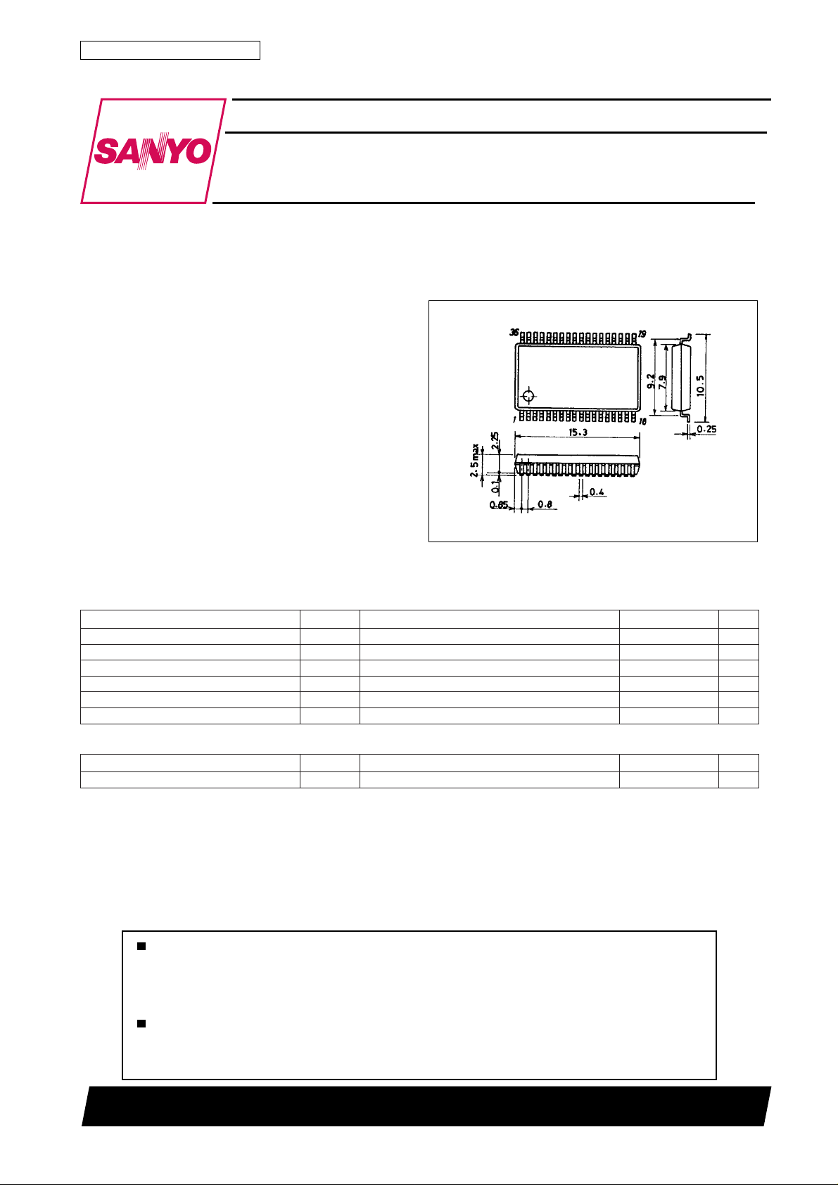
Package Dimensions
unit:mm
3129-MFP36S
[LB1813M]
SANYO : MFP36S
˚C
˚C
Allowable Operating Conditions at Ta = 25˚C
retemaraPlobmySsnoitidnoCsgnitaRtinU
egatlovylppuSV
Any and all SANYO products described or contained herein do not have specifications that can handle
applications that require extremely high levels of reliability, such as life-support systems, aircraft’s
control systems, or other applications whose failure can be reasonably expected to result in serious
physical and/or material damage. Consult with your SANYO representative nearest you before using
any SANYO products described or contained herein in such applications.
SANYO assumes no responsibility for equipment failures that result from using products at values that
exceed, even momentarily, rated values (such as maximum ratings, operating condition ranges,or other
parameters) listed in products specifications of any and all SANYO products described or contained
herein.
CC
SANYO Electric Co.,Ltd. Semiconductor Bussiness Headquaters
TOKYO OFFICE Tokyo Bldg., 1-10, 1 Chome, Ueno, Taito-ku, TOKYO, 110-8534 JAPAN
83198HA (KT)/50995TH (ID)/8112TS No.4183-1/8
5.6ot2.4V
Page 2

Electrical Characteristics at Ta = 25˚C, VCC=5V
LB1813M
retemaraPlobmySsnoitidnoC
niardtnerruC
tnerrucsaibrevoegnahcemiTI
1egatlovtupnirevoegnahcemiTV
2egatlovtupnirevoegnahcemiTV
tnerrucsaibS/SI
egatlovtratsS/SV
egatlovpotsS/SV
tnerructupnireifilpmasaibtceffe-llaHI
egnaregatlovtupniesahp-nIhV2.2V
egnaregatlovtupnilaitnreffiDfidV07002p-pVm
egatlovtesffotupnIohV 01±Vm*
egatlovtuptuotceffe-llaHV
tnerruckaeLI
egatlovnoitarutastuptuO
)ecruossulpknis(
tnerruckaeltuptuOI
retimiltnerruC1ferV72.003.033.0V
niagegatlovreifilpmalortnoCG
laitnreffidesahpniagegaltoV ∆G
tnerrucsaibreifilpmadetargetnIbil 1±Aµ
edutilpmaegatlovtuptuodetargetnI
htdiwdnabniaG 0001zHk*
egnaregatlovtupnireifilpmaGFVGF5001p-pVm
niagegatlovreifilpmaGFG
tesffotupnireifilpmaGFV
egatlovecnereferlanretnireifilpmaGFV
htdiwsiseretsyhttimhcS
levelnoitarepotupnittimhcShsV1V
rebmuntnuocerksiddeepSN 2401
egatlovlevelwoltuotnuocerksiDV
egatlovlevelhgihtuotnuocerksiDV
tnerruckaeltuotnuocerksiDI
ycneuqerfnoitarepotnuocerksiDF
egnarnoitallicsOF
tnerrucsaibxednII
egnaregatlovtupniesahp-nIVDI5.1V
egnartnerrucgnittessiseretsyHI
egatlovlevelwoltuptuoxednIV
egatlovlevelhgihtuptuoxednIV
egatlovnwod-karBV
egatlovlevelwoltuptuoyaleDV
egatlovlevelhgihtuptuoyaleDV
erutarepmetgnitareponwodtuhslamrehTDST051081*
htdiwsiseretsyH ∆ DST04*
I
1V
OCC
ICC1V
LS
S/S
S/S
S/S
BH
H
LH
LO
C
egatlovecnereferlanretnireifilpmadetargetnI2ferVV
C
+
iV
–
iV
GF
GF
∆ 1hsVhgiH → woL52Vm*
∆ 2hsVwoL → hgiH52Vm*
LD
HD
1 0.1±Aµ
D
D
BDI
ODI
LDI
HDI
CC
CC
LLS
HLS
IHAm5=5.18.1V
potS01±Aµ
1tasVIOV,A53.0=
2tasVIOV,A07.0=
0GF
B02.205.208.2V
I
D
I
D
CSO
VDIV5=4.0V
VDIV5=5.4V
VDIV5=05.2V
CDLD
VDIV5=4.0V
LLD
VDIV5=5.4V
HLD
)potS(V0.5=4.0Am
)ydaetS(V0.5=0203Am
V2.4=2.14.1V
CC
V2.4=5.10.2V
CC
2ferVfoecnereferhtiwAm5.0–=il57.0V
2ferVfoecnereferhtiwAm5.0=il4.1–V
poolnepO06Bd
Am5.0–=3.0V
Am5.0=V
Note : *) Marked values are guaranteed by the design itself and therefore do not require measurement.
sgnitaR
nimpytxam
08.0V
0.2V
08.0V
0.2V
CC
6–Bd
2/V
CC
CC
4.0–V
CC
50151Aµ
CC
tinUetoN
4.0Am
V
CC
1.0Am
V
CC
02Aµ
7.0–V
0.1±Am
1±Bd
01±Vm
1–V
0.1zHM*
0.1zHM*
01±Aµ
5.0–V
˚C
˚C
No.4183-2/8
Page 3

Block Diagram
LB1813M
Pin Assignment
Unit (reissitace : Ω, capacitance : F)
(Top view)
No.4183-3/8
Page 4

T ruth T able
LB1813M
ecruoS → kniS
1
2
3
4
5
6
When an high level exists for Hall-effect input.
U+>U
V+>V
W+>W
esahp-V → esahp-WHHL
esahp-V → esahp-U LHL
esahp-W → esahp-ULHH
esahp-W → esahp-VLLH
esahp-U → esahp-V HLH
esahp-U → esahp-WHLL
–
–
–
Pin Description
Pin No.
Symbol Pin voltage Equivalent circuit Pin function
5
6
7
8
9
10
–
W
+
W
–
V
+
V
–
U
+
U
2.2V min
–0.7V max
V
CC
tupnItceffE-llaH
UVW
Unit (resistance : Ω)
• W-phase Hall-effect input pin.
+>W–
is established when logic is at an high level.
W
• V-phase Hall-effect input pin.
+>V–
is established when logic is at an high level.
V
• U-phase Hall-effect input pin.
+>U–
is established when logic is at an high level.
U
11
12
HB
FC
1.5V typ
I
=5mA
H
• Minus pin for Hall-efffect bias,
When stopped, switches open and Hall-effect bias
severs.
• Frequency characteristics revision pin. By installing a
capacitor between this pin and GND, close-loop
oscillation for the current control system halts.
13
14
+
I
–
I
1.5V typ
–0.5V max
V
CC
• Index input pin.
When the I+ pin is at an low level, I1 operates with the
fixed current of I1=10µA and when at an high level, I1
does not flow.
Hysteresis width is determined by the resistor attached
externally to the I
15
SL1
High : 2.0V min
Low : 0.8V max
• Time changeover pin.
+
pin.
fosc=1MHz
SL2
SL1
16
SL2
High : 2.0V min
Low : 0.8V max
H
L
HL
mpr006mpr003
mpr027mpr063
FG : 60pulse/round
Continued to next page.
No.4183-4/8
Page 5

Continued from preceding page.
LB1813M
Unit (resistance : Ω)
Pin No.
17
18
19
20
21
Symbol Pin voltage Equivalent circuit Pin function
X1
X2
GND
ID
DT1
High : 4.5V min
Low : 0.4V max
(When V
ID
=5V)
• Reference clock generating pin.
• Ground pin.
Grounded as with pins 1 and 36.
• Index pulse output pin.
• Pin Connecting the external CR for the delay time
constant circuit.
22
23
25
26
27
DT2
DTO
FG0
FG
FG
• Break-down current setting pin for the delay time
constant circuit.
High : 4.5V min
Low : 0.4V max
(When V
–
+
2.48V
(When V
ID
ID
=5V)
=5V)
• Index delay pulse output pin.
• FG amplifier output pin.
• FG amplifier negative input pin.
• FG amplifier positive input pin.
Generates reference voltage within IC.
Continued to next page.
No.4183-5/8
Page 6

Continued from preceding page.
LB1813M
Unit (resistance : Ω)
Pin No.
28
29
30
31
32
Symbol Pin voltage Equivalent circuit Pin function
S/S
DO
IAI
IAO
VID
High : 2.0V min
Low : 0.8V max
• Start/Stop changeover pin.
Low level active.
• Speed discriminator output pin.
• Integrated amplifier input pin.
• Integrated amplifier output pin.
• Index pulse output and index delay pulse output power
supply pin.
For applications when V
equals 5V, VCC=VID=5V.
CC
33
34
35
36
1
2
3
4
V
CC
R
f
U
OUT
Pow GND
Sub GND
V
OUT
W
OUT
AGC
• Total power supply voltage pin except for V
Voltage must be stable and free of ripple and noise
interference.
• Output current detection pin.
By installing an Rf resistor between this pin and V
output current is detected as voltage. Voltage detection
at this pin activates the current limitter.
• U-phase output pin.
• Output transistor ground pin.
• Ground pin. Ground as with pins 19 and 36.
• V-phase output pin.
• W-phase output pin.
• AGC (Automatic gain control) pin.
Confrds Hall-efffect amplifier gain in response to Hall effect input-frequnecy.
.
ID
,
CC
No.4183-6/8
Page 7

Index and Timing Chart
LB1813M
When SL1=high level
When SL1=low level.
Using only the ID pulse involves shorting DT1 and DT2.
No.4183-7/8
Page 8

LB1813M
Specifications of any and all SANYO products described or contained herein stipulate the performance,
characteristics, and functions of the described products in the independent state, and are not guarantees
of the performance, characteristics, and functions of the described products as mounted in the customer’s
products or equipment. To verify symptoms and states that cannot be evaluated in an independent device,
the customer should always evaluate and test devices mounted in the customer’s products or equipment.
SANYO Electric Co., Ltd. strives to supply high-quality high-reliability products. However, any and all
semiconductor products fail with some probability. It is possible that these probabilistic failures could
give rise to accidents or events that could endanger human lives, that could give rise to smoke or fire,
or that could cause damage to other property. When designing equipment, adopt safety measures so
that these kinds of accidents or events cannot occur. Such measures include but are not limited to protective
circuits and error prevention circuits for safe design, redundant design, and structural design.
In the event that any and all SANYO products described or contained herein fall under strategic
products (including services) controlled under the Foreign Exchange and Foreign Trade Control Law of
Japan, such products must not be exported without obtaining export license from the Ministry of
International Trade and Industry in accordance with the above law.
No part of this publication may be reproduced or transmitted in any form or by any means, electronic or
mechanical, including photocopying and recording, or any information storage or retrieval system,
or otherwise, without the prior written permission of SANYO Electric Co. , Ltd.
Any and all information described or contained herein are subject to change without notice due to
product/technology improvement, etc. When designing equipment, refer to the “Delivery Specification”
for the SANYO product that you intend to use.
Information (including circuit diagrams and circuit parameters) herein is for example only ; it is not
guaranteed for volume production. SANYO believes information herein is accurate and reliable, but
no guarantees are made or implied regarding its use or any infringements of intellectual property rights
or other rights of third parties.
This catalog provides information as of August, 1998. Specifications and information herein are subject to
change without notice.
PS No.4183-8/8
 Loading...