

Page 1
Any and all SANYO products described or contained herein do not have specifications that can handle
applications that require extremely high levels of reliability, such as life-support systems, aircraft’s
control systems, or other applications whose failure can be reasonably expected to result in serious
physical and/or material damage. Consult with your SANYO representative nearest you before using
any SANYO products described or contained herein in such applications.
SANYO assumes no responsibility for equipment failures that result from using products at values that
exceed, even momentarily, rated values (such as maximum ratings, operating condition ranges,or other
parameters) listed in products specifications of any and all SANYO products described or contained
herein.
Monolithic Digital IC
Octal NPN Darlington-pair Transistor Array
Ordering number:ENN4094
LB1741
SANYO Electric Co.,Ltd. Semiconductor Company
TOKYO OFFICE Tokyo Bldg., 1-10, 1 Chome, Ueno, Taito-ku, TOKYO, 110-8534 JAPAN
Overview
The LB1741 is a high-current Darlington-pair transistor
array that incorporates output clamp diodes, making it ideal
for driving inductive loads.
The LB1741 with active-HIGH, 10.5kΩ impedance inputs
interfaces directly to P-MOS or CMOS logic. With an input voltage of –0.5 to 30V (max), outputs can sink 500mA
(max) per channel and have 50V (max) output withstand
voltage.
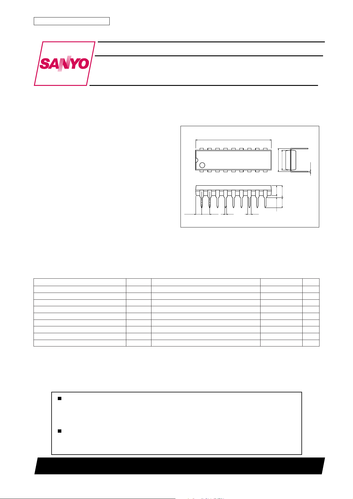
The LB1741 is available in 18-pin DIPs.
Features
• Output clamp diodes.
• Drives inductive loads.
• Active-HIGH, 10.5kΩ impedance inputs.
• Interfaces to P-MOS or CMOS logic.
• 500mA (max) per channel output current sink.
• 50V (max) output withstand voltage.
• 30V (max) input voltage.
• 18-pin DIP.
Specifications
Absolute Maximum Ratings at Ta = 25˚C
retemaraPlobmySsnoitidnoCsgnitaRtinU
egnaregatlovdnatshtiwtuptuOV
egatlovtupnIV
tnerructuptuOI
tnerrucDNGI
egatlovdnatshtiwedoidpmalCV
tnerrucdrawrofedoidpmalCI
noitapissidrewopelbawollAxamdP 74.1W
erutarepmetgnitarepOrpoT 58+ot04–
erutarepmetegarotSgtsT 051+ot55–
OEC
I
O
DNG
R
F
Package Dimensions
unit:mm
3007B-DIP18
[LB1741]
24.0
18
1
(1.84)
2.54
10
6.4
7.62
0.25
9
(3.25)
3.85max
3.3
1.20.5
0.51min
SANYO : DIP18
05+ot5.0–V
03+ot5.0–V
005Am
2.3A
05V
005Am
˚C
˚C
22801TN (KT)/N042TS No.4094–1/4
Page 2
Recommended Operating Ranges at Ta = 25˚C
retemaraPlobmySsnoitidnoC
egnaregatlovdnatshtiwtuptuOV
egatlovtupnIV
tnerructuptuOI
egatlovdnatshtiwedoidpmalCV
tnerrucdrawrofedoidpmalCI
OEC
I
O
R
F
Electrical Characteristics at Ta = 25˚C
retemaraPlobmySsnoitidnoC
V
egatlovtupniNO-nruTV
tnerructupniNOrotsisnarTI
tnerructupniFFOrotsisnarTI
niagtnerrucCDh
egatlovnoitarutastuptuOV
tnerrucegakaeltuptuOI
tnerrucegakaeledoidpmalCI
egatlovdrawrofedoidpmalCV
ecnaticapactupnIC
emityaledNO-nruTt
emityaledFFO-nruTt
V
)NO(I
V
V
VIV21=0.154.1Am
)NO(I
I
)FFO(I
O
V
EF
I
I
I
)tas(EC
I
I
O
V
XEC
V
VRV05= 05Aµ
R
I
F
F
I
RL521= Ω C,
NO
RL521= Ω C,
FFO
LB1741
sgnitaR
nimpytxam
005V
003V
stiucricthgie,elcycytud%8,sm52=WPT0004Am
stiucricthgie,elcycytud%52,sm52=WPT0002Am
sgnitaR
nimpytxam
I,V2=
EC
EC
EC
EC
Aµ005= 56Aµ
EC
V05= 05Aµ
EC
EC
Am053= 0.2V
Am521=0.5V
O
I,V2=
Am002=0.6V
O
I,V2=
Am572=0.7V
O
I,V2=
Am053=0.8V
O
I,V2=
Am053=0001
O
I,Aµ005=
Am053=3.16.1V
O
I,Aµ053=
Am002=1.13.1V
O
I,Aµ052=
Am001=9.01.1V
O
V,V05=
V1=005Aµ
I
04Fp
V,Fp51=
L
L
V05=1.0sµ
O
V,Fp51=
V05=2.0sµ
O
tinU
05V
004Am
tinU
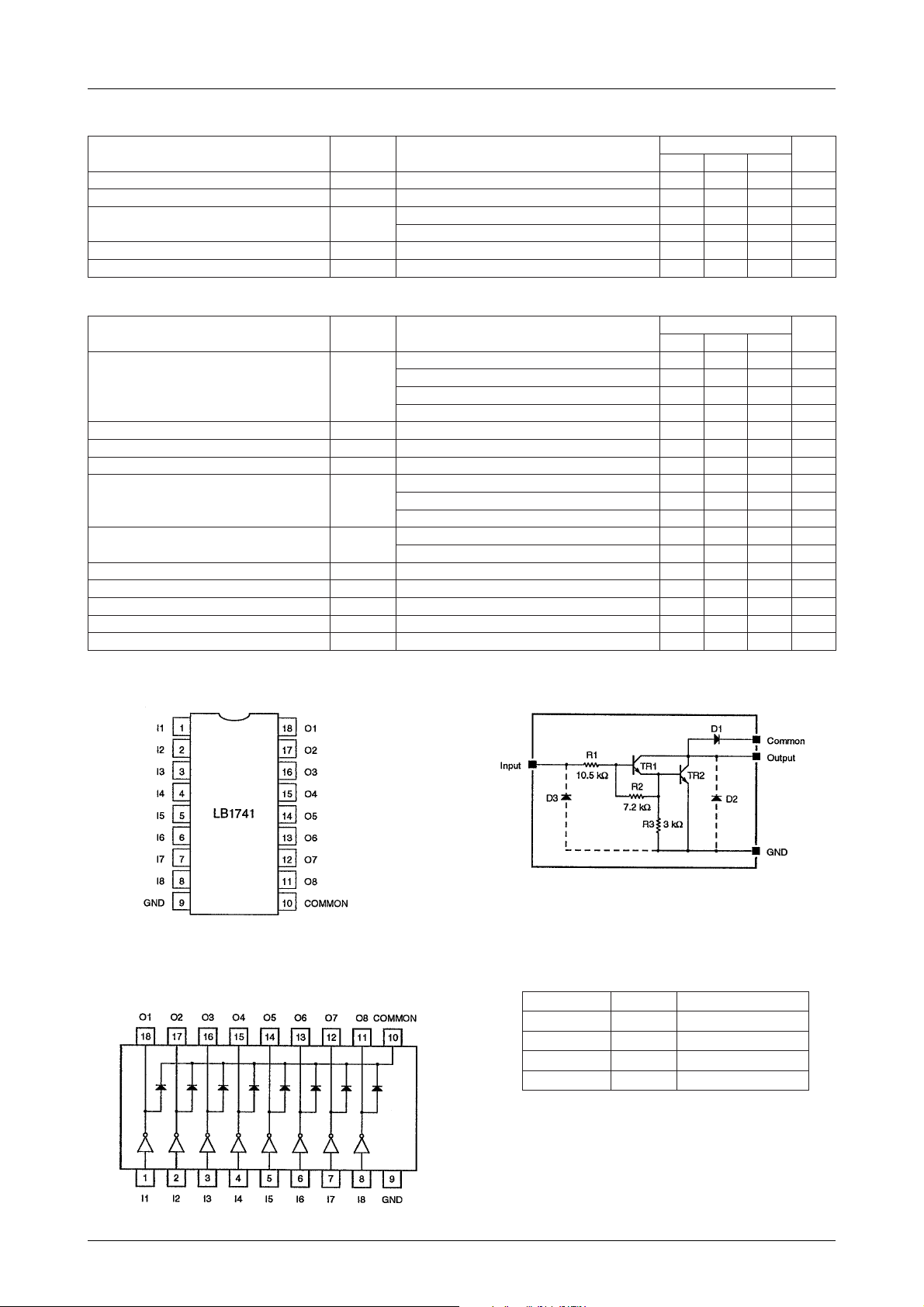
Pinout Equivalent Circuit
Notes
1. Only one channel is shown.
2. D2 and D3 are parasitic diodes.
Top view
Block Diagram Pin Function
rebmuNemaNnoitpircseD
8ot18Iot1IstupnirotsisnarT
9DNGdnuorG
01NOMMOCnommocrotsisnarT
81ot118Oot1OstuptuorotsisnarT
No.4094–2/4
Page 3
LB1741
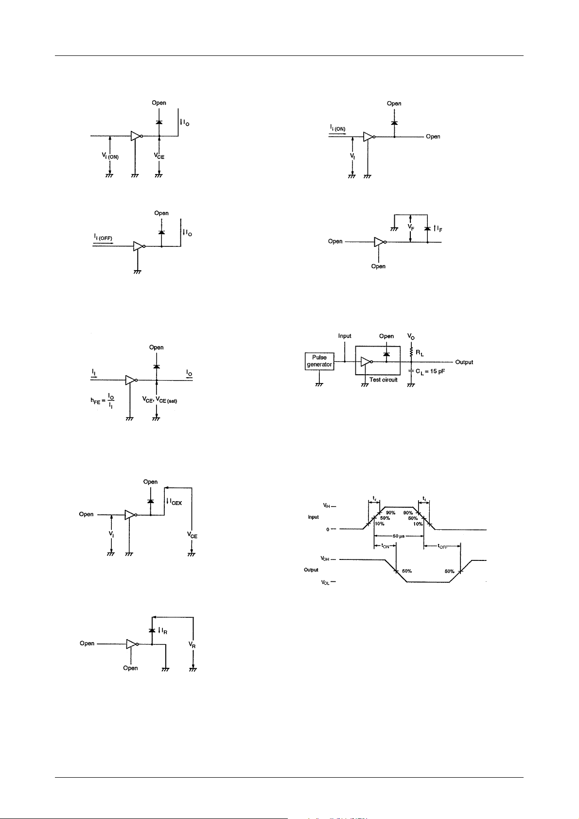
Measurement Circuits
Turn-ON input voltage ON-state input current
OFF-state input current Clamp diode forward voltage
DC current gain and output saturation voltage Turn-ON turn-OFF delay times
Output leakage current
Clamp diode leakage current
Notes
1. 50µs pulsewidth, 10% duty cycle, 50Ω pulse
generator ouput impedance, tr≤5ns, tf≤10ns,
VI=8V.
2. CL includes probe and jig capacitances.
No.4094–3/4
Page 4
LB1741
Specifications of any and all SANYO products described or contained herein stipulate the performance,
characteristics, and functions of the described products in the independent state, and are not guarantees
of the performance, characteristics, and functions of the described products as mounted in the customer's
products or equipment. To verify symptoms and states that cannot be evaluated in an independent device,
the customer should always evaluate and test devices mounted in the customer's products or equipment.
SANYO Electric Co., Ltd. strives to supply high-quality high-reliability products. However, any and all
semiconductor products fail with some probability. It is possible that these probabilistic failures could
give rise to accidents or events that could endanger human lives, that could give rise to smoke or fire,
or that could cause damage to other property. When designing equipment, adopt safety measures so
that these kinds of accidents or events cannot occur. Such measures include but are not limited to protective
circuits and error prevention circuits for safe design, redundant design, and structural design.
In the event that any or all SANYO products(including technical data,services) described or
contained herein are controlled under any of applicable local export control laws and regulations,
such products must not be exported without obtaining the export license from the authorities
concerned in accordance with the above law.
No part of this publication may be reproduced or transmitted in any form or by any means, electronic or
mechanical, including photocopying and recording, or any information storage or retrieval system,
or otherwise, without the prior written permission of SANYO Electric Co. , Ltd.
Any and all information described or contained herein are subject to change without notice due to
product/technology improvement, etc. When designing equipment, refer to the "Delivery Specification"
for the SANYO product that you intend to use.
Information (including circuit diagrams and circuit parameters) herein is for example only ; it is not
guaranteed for volume production. SANYO believes information herein is accurate and reliable, but
no guarantees are made or implied regarding its use or any infringements of intellectual property rights
or other rights of third parties.
This catalog provides information as of February, 2001. Specifications and information herein are subject
to change without notice.
PS No.4094–4/4
 Loading...