

Page 1
Any and all SANYO products described or contained herein do not have specifications that can handle
applications that require extremely high levels of reliability, such as life-support systems, aircraft’s
control systems, or other applications whose failure can be reasonably expected to result in serious
physical and/or material damage. Consult with your SANYO representative nearest you before using
any SANYO products described or contained herein in such applications.
SANYO assumes no responsibility for equipment failures that result from using products at values that
exceed, even momentarily, rated values (such as maximum ratings, operating condition ranges,or other
parameters) listed in products specifications of any and all SANYO products described or contained
herein.
Monolithic Digital IC
High-Voltage, Current-Sink Output Driver
Ordering number:ENN2846A
LB1731
SANYO Electric Co.,Ltd. Semiconductor Company
TOKYO OFFICE Tokyo Bldg., 1-10, 1 Chome, Ueno, Taito-ku, TOKYO, 110-8534 JAPAN
Overview
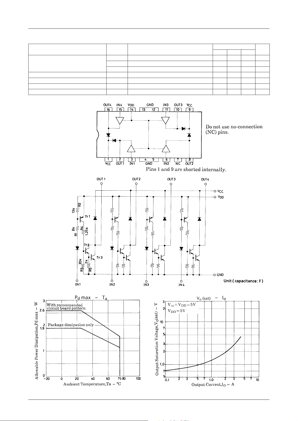
The LB1731 is a 4-channel high-voltage current sink output driver. Inputs are active-low CMOS/TTL logic-level,
and outputs are high-voltage open-collector NPN
Darlington pairs.
Each driver in the LB1731 sinks up to 1.5A and withstands
collector voltages of up to 85V.
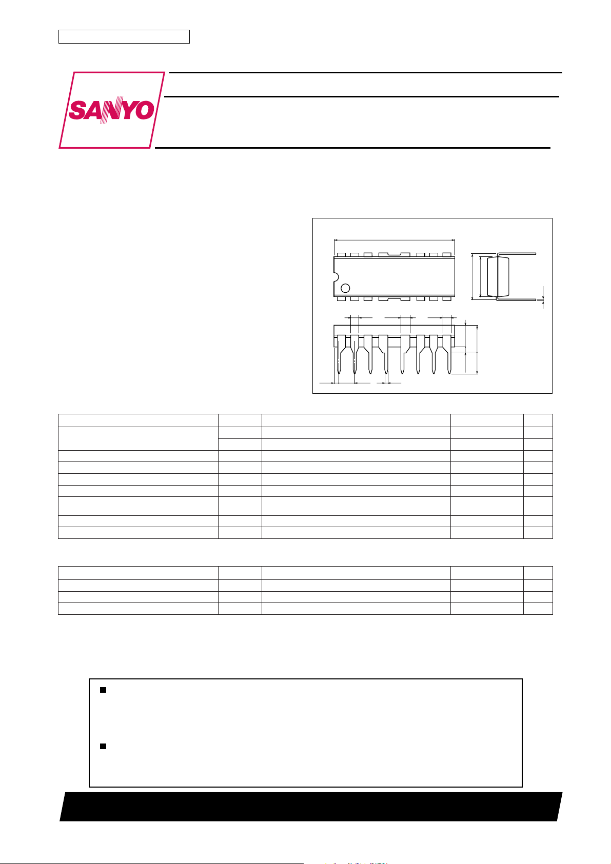
The LB1731 is available in a 16-pin DIP package.
Features
• For independent high-voltage high-current drivers.
• Output clamp diodes.
• Input protection diodes.
• 5V CMOS- and TTL-compatible logic-level inputs.
Specifications
Absolute Maximum Ratings at Ta = 25˚C
retemaraPlobmySsnoitidnoCsgnitaRtinU
V
xam 0.7V
egatlovylppusmumixaM
egatlovtuptuodeilppAV
egatlovtupnideilppAV
tnerructuptuOI
tnerrucdrawrofedoidpmalCI
noitapissidrewopelbawollAxamdP
erutarepmetgnitarepOrpoT 57+ot02–
erutarepmetegarotSgtsT 051+ot55–
DD
V
xam 28V
CC
xam 58V
O
xamVNI≥ DNG
NI
xam 5.1A
O
SF
W6.2
Package Dimensions
unit:mm
3054B-DIP16F
[LB1731]
19.0
16
(0.61)
1
1.3
1.65
2.54
0.5
1.25
9
6.45
7.62
0.4
8
(3.46)
4.26max
3.5
0.51min
SANYO : DIP16F
V
:nrettapdraobtiucricdednemmocerhtiwylnoegakcaP
Vot0.7–
0.01+
DD
DD
V
5.1A
9.1W
˚C
˚C
Allowable Operating Ranges at Ta = 25˚C
retemaraPlobmySsnoitidnoCsgnitaRtinU
egnaregatlovylppusrewoPV
egatlovlevel-NOtupnIV
egatlovlevel-FFOtupnIV
DD
noVNI≥ I,DNG
NI
ffoIO≤ Aµ03
NI
A0.1=
O
22801TN (KT)/N2195YK/D088YT, TS No.2846–1/3
0.7ot5.3V
V
V
Vot0.7–
6.2–
DD
DD
DD
Vot3.0–
DD
V
0.01+
V
Page 2
Electrical Characteristics at Ta = 25˚C, VDD=5.0V
retemaraPlobmySsnoitidnoC
VO1tasVNIV=
egatlovnoitarutastuptuO
egatlovniatsustuptuOV
tnerructupnII
egatlovdrawrofedoidpmalCV
tnerrucesreveredoidpmalCI
VO2tasVNIV=
VO3tasVNIV=
susIOAm001=58V
O
V
NI
SF
SR
DD
I
SF
V
CC
LB1731
sgnitaR
nimpytxam
I,V0.5–
DD
DD
DD
V,V0.7=
NIV=DD
A5.1= 0.3V
V,V28=
O
A5.0=2.1V
O
I,V0.5–
A0.1=5.1V
O
I,V0.5–
A5.1=0.2V
O
V0.7–5.0Am
V0=03Aµ
tinU
Equivalent Circuit
No.2846–2/3
Page 3

Recommended Circuit Board Layout
LB1731
Specifications of any and all SANYO products described or contained herein stipulate the performance,
characteristics, and functions of the described products in the independent state, and are not guarantees
of the performance, characteristics, and functions of the described products as mounted in the customer's
products or equipment. To verify symptoms and states that cannot be evaluated in an independent device,
the customer should always evaluate and test devices mounted in the customer's products or equipment.
SANYO Electric Co., Ltd. strives to supply high-quality high-reliability products. However, any and all
semiconductor products fail with some probability. It is possible that these probabilistic failures could
give rise to accidents or events that could endanger human lives, that could give rise to smoke or fire,
or that could cause damage to other property. When designing equipment, adopt safety measures so
that these kinds of accidents or events cannot occur. Such measures include but are not limited to protective
circuits and error prevention circuits for safe design, redundant design, and structural design.
In the event that any or all SANYO products(including technical data,services) described or
contained herein are controlled under any of applicable local export control laws and regulations,
such products must not be exported without obtaining the export license from the authorities
concerned in accordance with the above law.
No part of this publication may be reproduced or transmitted in any form or by any means, electronic or
mechanical, including photocopying and recording, or any information storage or retrieval system,
or otherwise, without the prior written permission of SANYO Electric Co. , Ltd.
Any and all information described or contained herein are subject to change without notice due to
product/technology improvement, etc. When designing equipment, refer to the "Delivery Specification"
for the SANYO product that you intend to use.
Information (including circuit diagrams and circuit parameters) herein is for example only ; it is not
guaranteed for volume production. SANYO believes information herein is accurate and reliable, but
no guarantees are made or implied regarding its use or any infringements of intellectual property rights
or other rights of third parties.
This catalog provides information as of February, 2001. Specifications and information herein are subject
to change without notice.
PS No.2846–3/3
 Loading...