

Page 1
Ordering number:EN3295
Monolithic Digital IC
LB1693
3-Phase Brushless Motor Driver
Overview
The LB1693 is a driver IC for 3-phase brushless motors.
It is ideally suited for office automation equipment and
DC fan motors.
Features
• 3-Phase brushless motor driver.
• 45V withstand voltage and 2.5A output current.
• PWM switch regulator control section.
• Current limitter.
• Overvoltage and overcurrent protection circuit.
• Thermal shutdown cirucit.
• Hall amp with hysteresis characteristic.
Specifications
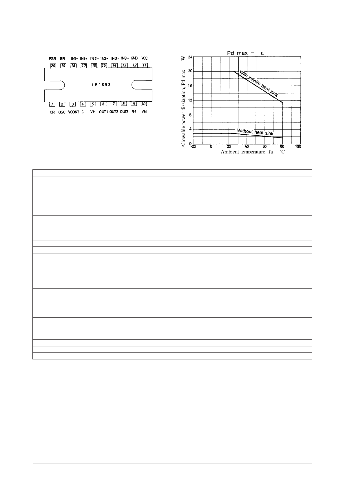
Absolute Maximum Ratings at Ta = 25˚C
retemaraPlobmySsnoitidnoCsgnitaRtinU
egatlovylppusmumixaM
tnerructuptuOmumixaMI
noitapissidrewopelbawollAxamdP
erutarepmetgnitarepOrpoT 08+ot02–
erutarepmetegarotSgtsT 051+ot55–
Allowable Operating Conditions at Ta = 25˚C
retemaraPlobmySsnoitidnoCsgnitaRtinU
egatlovylppuS
tnerructuptuorotalugeregatloVI
V
H
egatlovylppusV
tnerructuptuorotarapmoCI
V
xam 54V
CC
VMxam 54V
O
V
CC
V
M
HV
H
CSO
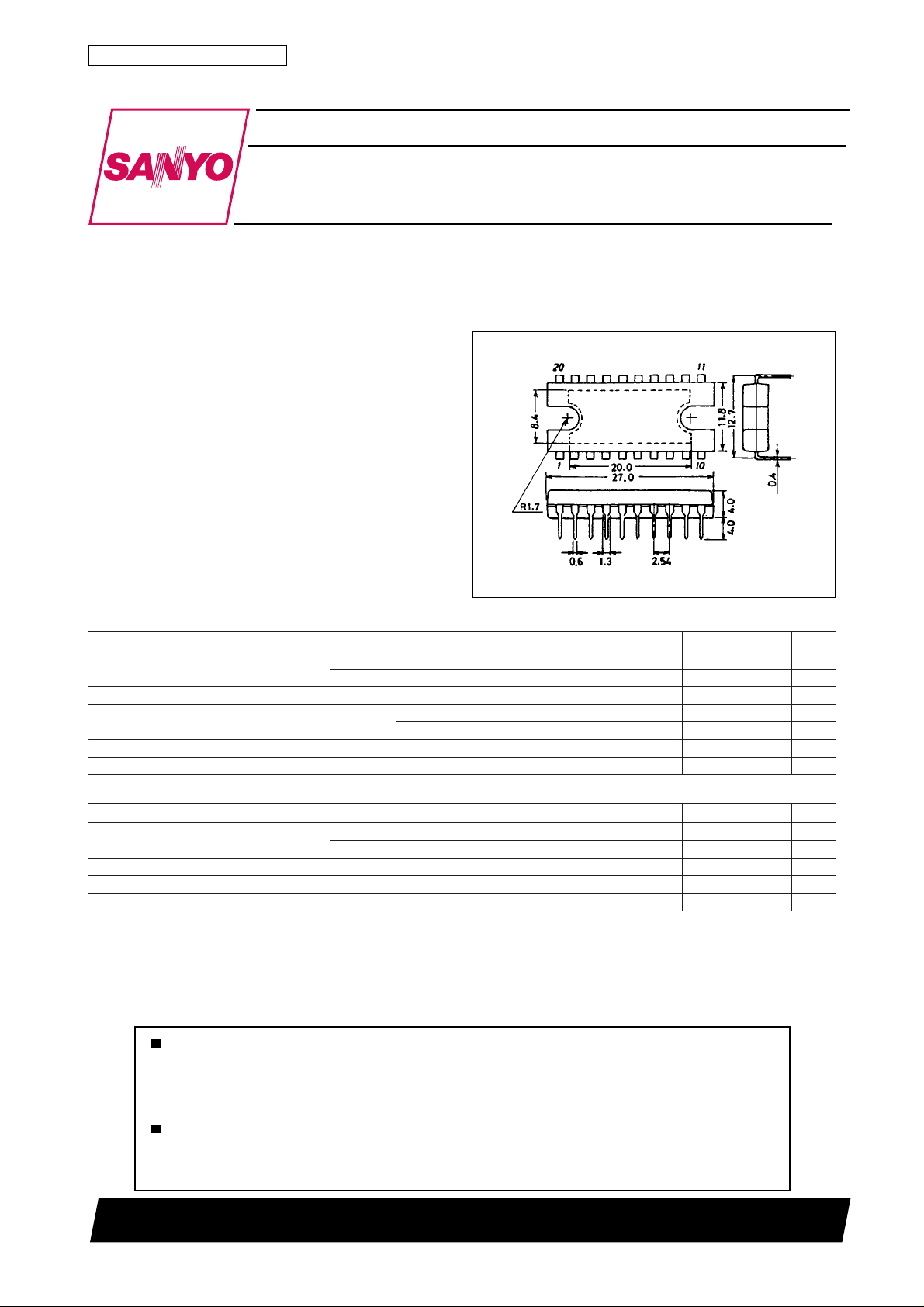
Package Dimensions
unit:mm
3037A-DIP20H
[LB1693]
SANYO : DIP20H
5.2A
CItnednepednI 3W
knistaehetnifnihtiW 02W
˚C
˚C
63ot9V
VH14otV
02ot0Am
5.5ot5.4V
03ot0Am
Any and all SANYO products described or contained herein do not have specifications that can handle
applications that require extremely high levels of reliability, such as life-support systems, aircraft’s
control systems, or other applications whose failure can be reasonably expected to result in serious
physical and/or material damage. Consult with your SANYO representative nearest you before using
any SANYO products described or contained herein in such applications.
SANYO assumes no responsibility for equipment failures that result from using products at values that
exceed, even momentarily, rated values (such as maximum ratings, operating condition ranges,or other
parameters) listed in products specifications of any and all SANYO products described or contained
herein.
SANYO Electric Co.,Ltd. Semiconductor Bussiness Headquaters
TOKYO OFFICE Tokyo Bldg., 1-10, 1 Chome, Ueno, Taito-ku, TOKYO, 110-8534 JAPAN
83198HA (KT)/4250TA, TS(GTPS) No.3295-1/9
Page 2
LB1693
Electrical Characteristics at Ta = 25˚C, VCC=VM=24V
retemaraPlobmySsnoitidnoC
tnerrucylppuS
egatlovnoitarutastuptuO
tnerrucegakaeltuptuOI
egatlovtuptuorotalugeregatloVV
noitautculfdaolrotalugeregatloV ∆V
noitautculfdaolrotalugeregatloV ∆V
tneiciffeocerutarepmetrotalugeRegatloV 2–
]pmallaH[
tnerrucsaibtupnII
egnaregatlovtupniedom-nommoC 5.1V
htdiwsiseretsyH ∆V
egatlovtupnihgihotwoLV
egatlovtupniwolothgiHV
rotallicsO
egatlovtuptuolevel-hgiH 54.3V
egatlovtuptuolevel-woL 0.1V
ycneuqerfnoitallicsOfk63=R Ω Fp0074=C,01zHk
edutilpmA 1.254.28.2p-pV
tneiciffeocerutarepmeT ∆f 1.0
rotarapmoC
egatlovtuptuOV
emitgnisiRrt 5.0sµ
emitgnillaFft 5.0sµ
esreveR/potS/drawroF
drawroFV
potSV
esreveRV
ffonoitarepoekarBV
nonoitarepoekarBV
retimiltnerruC
1retimiLRVf124.05.06.0V
2retimLRVf243.04.084.0V
egaltovnoitcetorpegatlovrevOV
htdiwsiseretsyH ∆V
erutarepmetnwodtuhslamrehTDSTtegratngiseD051081
htdiwsiseretsyH ∆ DST 52
egatlovnoitcetorpegatlov-woLV
htdiwsiseretsyH ∆V
egatlovedoidreppUV
ICC1edompotS58Am
ICC2Am5=tnerrucllaH5112Am
VO1tasIOV,A1=
VO2tasIOV,A2=
kael 001Aµ
O
I
H
HV
V
1H
CC
I
2H
HV
BH
NI
HLS
LHS
I
CSO
RSF
RSF
RSF
1 8.0V
RB
20.2V
RB
F
CSO
1 08.0V
21.25.29.2V
32.40.5V
DSVO
DSVO
DSVL
DSVL
IOA1=8.08.27.4V
V+
)knis(O
V+
)knis(O
Am01=5.60.75.7V
V63ot5.9=07002Vm
Am02ot0=041052Vm
Am03=1.15.1V
)ecruos(O
)ecruos(O
nimpytxam
sgnitaR
1.20.3V
0.32.4V
14Aµ
H
828364Vm
80223Vm
23–02–8–Vm
83245.44V
8.03.18.1V
6.30.44.4V
40.011.081.0V
tinU
mV/˚C
8.1-V
%/˚C
˚C
˚C
No.3295-2/9
Page 3
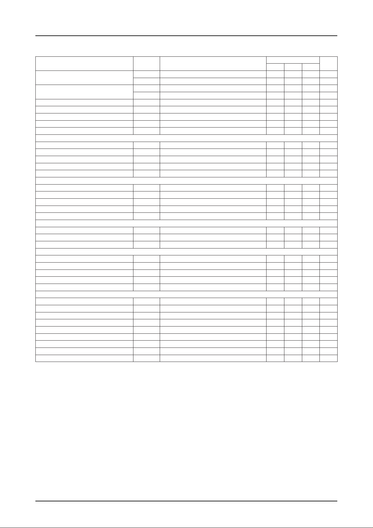
Pin Assignment
Pin Description
+
1NI
+
2NI
+
3NI
1TUO
2TUO
3TUO
V
CC
V
M
R
f
DNG
B
R
RSF02.niplortnocesreveR/potS/drawroF
V
H
RC1 /rotalugergnihctiwsehtrofycneuqerfnoitallicsoehtsteS
CSO2 .tuptuorotcellocnepo;deslupdellortnoc-ytudstuptuO
V
TNOC
C4 .2retimiltnerrucfonoitarepognirudtnerrucrotomehtniselppirsesserppuS
emaNniP.oNniPnoitpircseD
–
1NI,
–
2NI,
–
3NI,
81,71
61,51
41,31
6
7
8
11 .noitcestuptuonahtrehtonoitceshcaeotegatlovgniylpparofnipylppusrewoP
01.noitcestuptuorofylppusrewoP
9R;niptcetedtnerructuptuO
21
91
5stnemelellaHrofniprewoP
3 .egaltovtuptuorotalugergnichtiwsehtseirav;niplortnocdeepS
LB1693
+
1NInehwetatsehtsicigolhgiH
1NInehwetatsehtsicigol”hgiH
+
1NInehwetatsehtsicigolhgiH
.1esahProfniptuptuO
.2esahProfniptuptuO
.3esahProfniptuptuO
.egatlova
nipekarB
V8.0ot0:drawroF
V9.2ot1.2:potS
f
tuptuorehtorofdnuorG
V0.5ot2.4:esreveR
.1esahProfsniptupnitnemelellaH:1TUO
1NI>–.
.2esahProfsniptupnitnemelellaH:2TUO
+
1NI>–.
.3esahProfsniptupnitnemelellaH:3TUO
1NI>–.
satnerructuptuoehttcetedotdnuorgdnanipsihtneewtebdetresnisi
RehttasirotsisnarttuptuofolaitnetopmuminimehT
.nip
f
.)sselroV8.0(wol/)eromroV2(hgihnipsihtgnittesybffo/nodehctiwssiekarbehT
.nipsihttaegatlovehtotgnidroccaesreverninevirdro,deppots,drawrofnevirdsirotomehT
V:ylppusrewop)dezilibats(lanretniehtgnisunehW
V:ylppusrewop)dezilibats(lanretxeehtgnisunehW
.pytV7=
H
.pytV5=
H
No.3295-3/9
Page 4

Truth T able
LB1693
Block Diagram and Peripheral Circuit Diagram
PWM control (1)
No.3295-4/9
Page 5

PWM control (2)
LB1693
No.3295-5/9
Page 6

VCC=VH=5V PMW control
LB1693
No.3295-6/9
Page 7

VCC=5V , VM are No speed control
LB1693
1. Switching regulator oscillation circuit (PWM generation circuit)
1-1. Oscillation circuit (40 to 50kHz max.)
Figure 1 shows the oscillation circuit that generates the
triangular waves. The oscillation frequency for this circuit
is detemined by the following equation (with VH=7V typ.)
1
f=
t0 + t
(Hz)
1
t0~0.56CR (charging)
t1~1.34CRN (discharging)
(RN is the internal resistance of 1.4kΩ approx.)
In actual applications, R >> RN is used to suppress the influence
of variation in the IC’s internal resistance.
Figure 1 Oscillation Circuit
No.3295-7/9
Page 8

LB1693
1-2. Comparator circuit
Figure 2 shows the comparator circuit for comparing the triangular wave output, the speed control
signal, etc.
input terminals
CR Input the triangular wave output.
V
C Goes high when current limiter 2 is operating.
(When V
2. Position detection circuit (Hall element input circuit)
The position detection circuit is a differential amp with hysteresis (38mV typ.). For the operating DC level,
use within the common-mode phase input voltage range (1.5 to VH–1.8V). Also it is recommended that the
input level is at least three times (150 to 200mVp-p) the hysteresis.
Input the speed control signal.
CONT
> V
C(H)
CR(H)
, the OSC output is off.)
Figure 2 Comparator Circuit
3. VH power supply circuit
The VH power supply pins can be used to from the internal power supply or an external power supply.
When using the internal power supply, the internal logic operates with VH=7V typical (VCC=24V). When using
an external power supply, set VCC=VH=5V and operate the internal logic at 5V.
4. Current limiter circuits
4-1. Current limiter 1
The current is limited by moving the sink side transistor from saturated to undaturated, so ASO can be
a problem.
I =
VRf1
(A)
R
f
Therefore, design so that as much as possible current limiter 1 is not triggered.
Also, take particular care not to exceed the maximum output current (2.5A) when current limiter 1 is
triggered.
4-2. Current limiter 2
This circuit limits the current by lowering the PWM output duty, thus lowering the VM voltage.
When current limiter 2 is triggered, the output current is no greater than 2A.
VRf2
I =
R
f
When not controlling the PWM, add a current limiter to the VM power supply. (A current setting no
greater than 60% to 70% of the current value of current limiter 1 and a short delay time are
recommended.)
5. Protection circuits
5-1. Overvoltage protection circuit
If the voltage at the VCC pin rises above the regulated votlage (38V), PWM output is inhibited and the
sink side output driver is switched off.
5-2. Low-votlage protection circuit
If the voltage at the VCC pin falls below the regulated voltage, just as in 5-1, PWM output is inhibited
and the sink side output driver is switched off.
5-3. Thermal shutdown circuit
If the junction temperature rises above the regulated temperature, just as in 5-1, PMW output is
inhibited and the sink output driver is switched off.
No.3295-8/9
Page 9

LB1693
6. Minimum voltage at VM power
Use a voltage greater than the VH voltage for the VM power supply votlage
VM≥V
H
Specifications of any and all SANYO products described or contained herein stipulate the performance,
characteristics, and functions of the described products in the independent state, and are not guarantees
of the performance, characteristics, and functions of the described products as mounted in the customer’s
products or equipment. To verify symptoms and states that cannot be evaluated in an independent device,
the customer should always evaluate and test devices mounted in the customer’s products or equipment.
SANYO Electric Co., Ltd. strives to supply high-quality high-reliability products. However, any and all
semiconductor products fail with some probability. It is possible that these probabilistic failures could
give rise to accidents or events that could endanger human lives, that could give rise to smoke or fire,
or that could cause damage to other property. When designing equipment, adopt safety measures so
that these kinds of accidents or events cannot occur. Such measures include but are not limited to protective
circuits and error prevention circuits for safe design, redundant design, and structural design.
In the event that any and all SANYO products described or contained herein fall under strategic
products (including services) controlled under the Foreign Exchange and Foreign Trade Control Law of
Japan, such products must not be exported without obtaining export license from the Ministry of
International Trade and Industry in accordance with the above law.
No part of this publication may be reproduced or transmitted in any form or by any means, electronic or
mechanical, including photocopying and recording, or any information storage or retrieval system,
or otherwise, without the prior written permission of SANYO Electric Co. , Ltd.
Any and all information described or contained herein are subject to change without notice due to
product/technology improvement, etc. When designing equipment, refer to the “Delivery Specification”
for the SANYO product that you intend to use.
Information (including circuit diagrams and circuit parameters) herein is for example only ; it is not
guaranteed for volume production. SANYO believes information herein is accurate and reliable, but
no guarantees are made or implied regarding its use or any infringements of intellectual property rights
or other rights of third parties.
This catalog provides information as of August, 1998. Specifications and information herein are subject to
change without notice.
PS No.3295-9/9
 Loading...