

Page 1
Ordering number : EN4844
73098HA (OT)/63094TH (OT) A8-8679 No. 4844-1/5
Overview
The LB1692 is a three-phase brushless motor driver IC. It
is optimal for use with DC fan motors in equipment such
as air conditioners or water heaters. The LB1692 is a highbreakdown voltage version of the LB1690.
Functions and Features
• Three-phase brushless motor driver
• 60 V breakdown voltage, 2.5 A output current
• Built-in current limiter
• Built-in low voltage protection circuit
• Built-in thermal protection circuit
• Built-in Hall amplifier with hysteresis
• FG output function
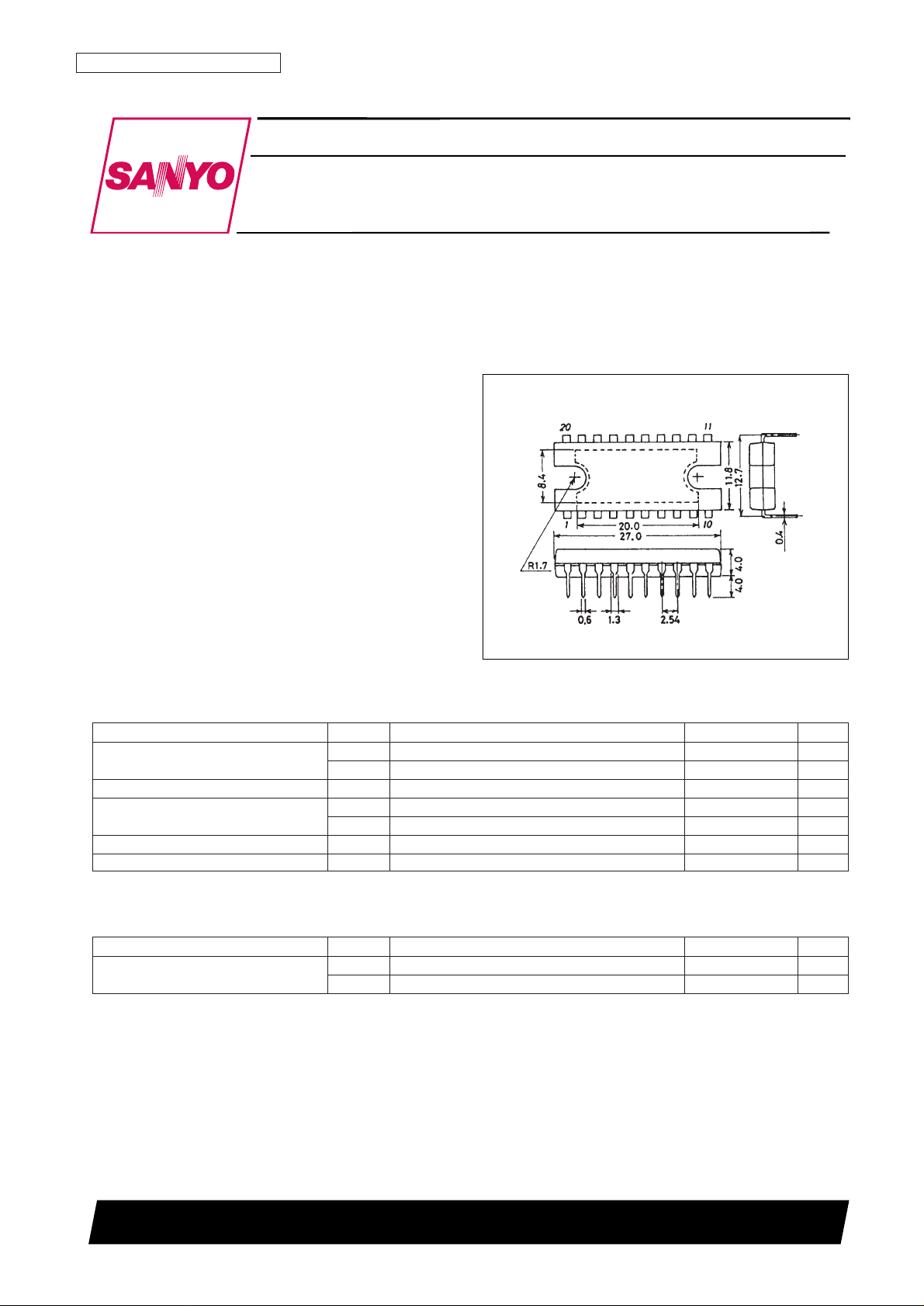
Package Dimensions
unit: mm
3037A-DIP20H
SANYO: DIP20H
[LB1692]
LB1692
SANYO Electric Co.,Ltd. Semiconductor Bussiness Headquarters
TOKYO OFFICE Tokyo Bldg., 1-10, 1 Chome, Ueno, Taito-ku, TOKYO, 110-8534 JAPAN
Three-Phase Brushless Motor Driver
Monolithic Digital IC
Specifications
Absolute Maximum Ratings at Ta = 25°C
Allowable Operating Ranges at Ta = 25°C
Parameter Symbol Conditions Ratings Unit
Maximum supply voltage
V
CC
max 10 V
V
M
max 60 V
Output current I
O
2.5 A
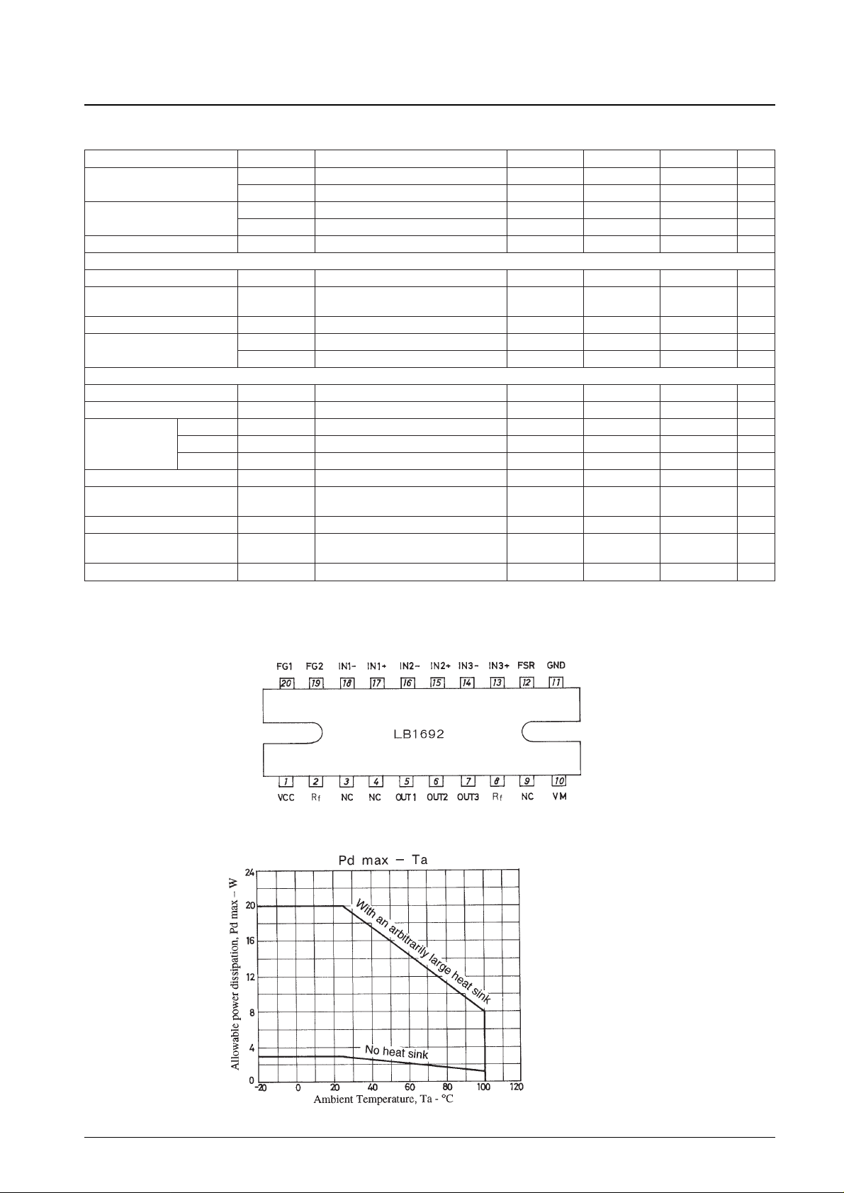
Allowable power dissipation
Pd max1 Independent IC 3 W
Pd max2 With an arbitrarily large heat sink 20 W
Operating temperature Topr –20 to +100 °C
Storage temperature Tstg –55 to +150 °C
Parameter Symbol Conditions Ratings Unit
Supply voltage range
V
CC
4.5 to 5.5 V
V
M
5 to 56 V
Page 2
Electrical Characteristics at Ta = 25°C, VCC= 5 V, VM= 45 V
Pin Assignment
No. 4844-2/5
LB1692
Parameter Symbol Conditions min typ max Unit
Current drain
I
CC1
When stopped 4 6 mA
I
CC2
10 15 mA
Output saturation voltage
V
O
sat1 IO= 1 A, VO(sink) + VO(source) 2.1 3.0 V
V
O
sat2 IO= 2 A, VO(sink) + VO(source) 3.0 4.2 V
Output leakage current I
O
leak 100 µA
[Hall amplifier]
Input bias current I
HB
1 4 µA
Common mode input voltage
1.5 3.2 V
range
Hysteresis ∆V
IN
23 30 37 mV
Input voltage
V
SLH
L → H 5 15 25 mV
V
SHL
H → L –25 –15 –5 mV
[FG pin] (Speed pulse output)
Output low level voltage V
FGL
IFG= 5 mA 0.16 0.4 V
Pull-up resistance R
FG
7.5 10 12.5 kΩ
Forward, reverse,
Forward V
FSR1
0 0.8 V
and stop Stop V
FSR2
2.1 2.5 2.9 V
operation
Reverse V
FSR3
4.2 5.0 V
Current control operation limiter V
Rf
0.42 0.5 0.6 V
Thermal cutoff operating
T
SD
Design target value 150 180 °C
temperature
Hysteresis ∆T
SD
25 °C
Low voltage protection
V
LVSD
3.5 3.8 4.1 V
operating voltage
Hysteresis ∆V
LVSD
0.2 0.3 0.4 V
(Top view)
Page 3

Truth Table
FSR
Forward: L (0 to 0.8 V)
Reverse: H (4.2 to 5.0 V)
FG Output
Block Diagram and Peripheral Circuits
No. 4844-3/5
LB1692
Item Source → Sink
Input
Forward/Reverse Control
IN1 IN2 IN3
FSR
1
OUT3 → OUT2
H H L
L
OUT2 → OUT3 H
2
OUT3 → OUT1
H L L
L
OUT1 → OUT3 H
3
OUT2 → OUT3
L L H
L
OUT3 → OUT2 H
4
OUT1 → OUT2
L H L
L
OUT2 → OUT1 H
5
OUT2 → OUT1
H L H
L
OUT1 → OUT2 H
6
OUT1 → OUT3
L H H
L
OUT3 → OUT1 H
Page 4

No. 4844-4/5
LB1692
Pin Functions
1. Position Detection Circuit (Hall device input circuit)
The position detection circuit is a differential amplifier with hysteresis (typically 30 mV).
Voltages within the common mode input voltage range (1.5 V to VCC– 1.8 V) should be used as the operating DC level.
We recommend using an input level that is more than three times the hysteresis, i.e., on the order of 120 to 160 mVp-p.
2. Current Control Circuit
Current control is performed by switching the sink side transistor from the saturated to the unsaturated range.
Therefore, it is possible for ASO to be a problem.
I = (A)
Therefore, if at all possible, applications should be designed so that the current limiter does not operate. Also, be
especially careful to design applications so that the maximum output current (2.5 A) is not exceeded when the
current limiter operates. Note that a current limiter must be added to the VMpower supply. (We recommend a current
limiter with a short delay time and with a design current that is about 60 to 70% of the current control circuit's
current value.)
3. Protection Circuits
• Low voltage protection circuit
The sink side output drivers are turned off if the VCCpin voltage falls below the stipulated range. This circuit is
provided to prevent incorrect operation.
• Thermal cutoff protection circuit
If the junction temperature exceeds the stipulated temperature range, the sink side output drivers are turned off.
This is identical to the operation of the circuit described in 3-1 above.
4. VMpower supply minimum voltage
The VMpower supply voltage should be greater than or equal to the VCCvoltage.
VM≥ V
CC
5. FG Output Circuit
The position detection inputs IN1, IN2, and IN3 are combined and the output is generated using waveform shaping.
The frequencies of those outputs are proportional to the rotational speed signal, and, as seen from the position
detectors, are equal to the input frequency itself (FG1) and three times the input frequency (FG2).
V
Rf
Rf
Pin Pin No. Function
IN1+, IN1– 17, 18 OUT1: A logic high level indicates that the Hall device input pins are in the state IN+ > IN-.
IN2+, IN2– 15, 16 OUT2: A logic high level indicates that the Hall device input pins are in the state IN+ > IN-.
IN3+, IN3– 13, 14 OUT3: A logic high level indicates that the Hall device input pins are in the state IN+ > IN-.
OUT1 5 Output pin 1
OUT2 6 Output pin 2
OUT3 7 Output pin 3
V
CC
1 Power supply for all sections other than the output block
V
M
10 Power supply that provides the output power
Rf 2, 8
Output current detection pin. The output current is converted to a voltage for detection by a resistor connected
between this pin and GND.
GND 11
Ground for all sections other than the output block
The Rf pin voltage will be the lowest output transistor potential.
Forward/stop/reverse control pin
The voltage on this pin controls the IC forward, stop, or reverse operation.
FSR 12 Forward: 0 to 0.8 V
Stop: 2.1 to 2.9 V
Reverse: 4.2 to 5.0 V
FG1 20 Speed pulse output pin 1. A pull-up resistor is built in.
FG2 19 Speed pulse output pin 2. A pull-up resistor is built in.
Page 5

PS No. 4844-5/5
LB1692
This catalog provides information as of July, 1998. Specifications and information herein are subject to change
without notice.
■ No products described or contained herein are intended for use in surgical implants, life-support systems, aerospace
equipment, nuclear power control systems, vehicles, disaster/crime-prevention equipment and the like, the failure of
which may directly or indirectly cause injury, death or property loss.
■ Anyone purchasing any products described or contained herein for an above-mentioned use shall:
➀ Accept full responsibility and indemnify and defend SANYO ELECTRIC CO., LTD., its affiliates, subsidiaries and
distributors and all their officers and employees, jointly and severally, against any and all claims and litigation and all
damages, cost and expenses associated with such use:
➁ Not impose any responsibility for any fault or negligence which may be cited in any such claim or litigation on
SANYO ELECTRIC CO., LTD., its affiliates, subsidiaries and distributors or any of their officers and employees
jointly or severally.
■ Information (including circuit diagrams and circuit parameters) herein is for example only; it is not guaranteed for
volume production. SANYO believes information herein is accurate and reliable, but no guarantees are made or implied
regarding its use or any infringements of intellectual property rights or other rights of third parties.
 Loading...