

Page 1
Ordering number:EN3294
Monolithic Digital IC
LB1690
3-Phase Motor Driver
Overview
The LB1690 is a driver IC for 3-phase brushless motors.
It is ideally suited for DC fan motors of air-conditioner,
hotwater system.
Features
• 3-Phase brushless motor driver.
• 45V withstand voltage and 2.5A output current.
• Current limiter.
• Low-voltage protection circuit.
• Thermal shutdown circiut.
• Hall amp with hysteresis characteristic.
• FG output function.
Specifications
Absolute Maximum Ratings at Ta = 25˚C
retemaraPlobmySsnoitidnoCsgnitaRtinU
egatlovylppusmumixaM
tnerructuptuOI
noitapissidrewopelbawollA
erutarepmetgnitarepOrpoT 001+ot02–
erutarepmetegarotSgtsT 051+ot55–
Allowable Operating Conditions at Ta = 25˚C
retemaraPlobmySsnoitidnoCsgnitaRtinU
egniaregatlovylppuS
V
xam 01V
CC
VMxam 54V
O
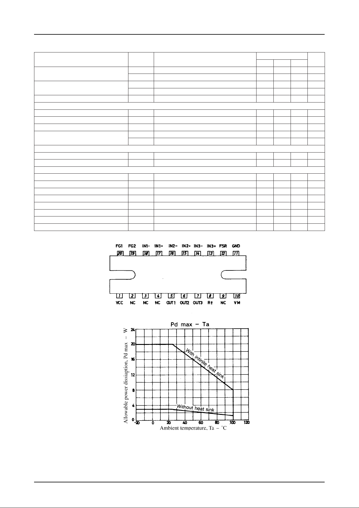
1xamdPCItnednepednI 3W
2xamdPknistaehetnifnihtiW 02W
V
CC
V
M
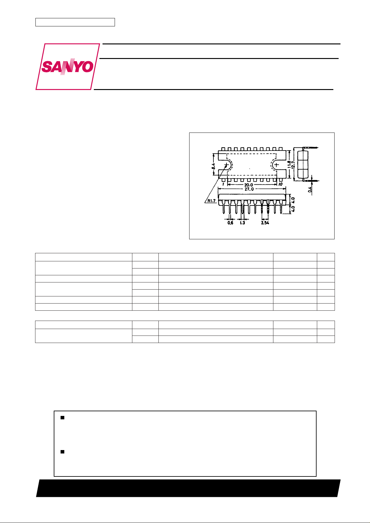
Package Dimensions
unit:mm
3037A-DIP20H
[LB1690]
SANYO : DIP20H
5.2A
˚C
˚C
5.5ot5.4V
24ot5V
Any and all SANYO products described or contained herein do not have specifications that can handle
applications that require extremely high levels of reliability, such as life-support systems, aircraft’s
control systems, or other applications whose failure can be reasonably expected to result in serious
physical and/or material damage. Consult with your SANYO representative nearest you before using
any SANYO products described or contained herein in such applications.
SANYO assumes no responsibility for equipment failures that result from using products at values that
exceed, even momentarily, rated values (such as maximum ratings, operating condition ranges,or other
parameters) listed in products specifications of any and all SANYO products described or contained
herein.
SANYO Electric Co.,Ltd. Semiconductor Bussiness Headquaters
TOKYO OFFICE Tokyo Bldg., 1-10, 1 Chome, Ueno, Taito-ku, TOKYO, 110-8534 JAPAN
82098HA (KT)/4240TA, TS(GTPS) No.3294-1/5
Page 2
LB1690
Electrical Characteristics at Ta = 25˚C, VCC=5V, VM=30V
retemaraPlobmySsnoitidnoC
tnerrucylppuS
egatlovnoitarutastuptuO
tnerrucegakaeltuptuOI
]reifilpmallaH[
tnerrucsaibtupnII
egnaregatlovtupniedom-nommoC 5.12.3V
htdiwsiseretsyH ∆V
egatlovtupnI
tuptuoeslupdeepS]lanimretGF[
egaltovtuptuolevel-woLV
eulavecnatsiserpu-lluPR
]esreveR/potS/drawroF[
drawroFV
potSV
esreveRV
retimiltnerruCV
erutarepmetnwodtuhslamrehTDSTtegratngiseD051081
htdiwsiseretsyH ∆ DST 52
egatlovnoitcetorpegatlov-woLV
htdiwsiseretsyH ∆V
Pin Assignment
ICC1edompotS5.35Am
ICC2 0151Am
VO1tasIOVA1=
VO2ttasIOVA2=
kael 001Aµ
O
BH
NI
V
V
]L[ → ]H[55152Vm
HLS
]H[ → ]L[52–51–5–Vm
LHS
I
LGF
GF
GF
1RSF
2RSF
3RSF
fR
DSVL
DSVL
V+)knis(
O
V+)knis(
O
Am5=61.04.0V
)ecruos(1.20.3V
O
)ecruos(0.32.4V
O
sgnitaR
nimpytxam
14Aµ
320373Vm
5.7015.21kΩ
08.0V
1.25.29.2V
2.40.5V
24.05.06.0V
5.38.31.4V
2.03.04.0V
tinU
˚C
˚C
(Top view)
No.3294-2/5
Page 3

T ruth Tab le
LB1690
FG Output
Block Diagram and Peripheral Circuit Diagram
FSR
Forward L 0 to 0.8V
Reverse H 4.2 to 5.0V
No.3294-3/5
Page 4

Pin Description
+
1NI
+
2NI
+
3NI
1TUO
2TUO
3TUO
V
CC
V
M
R
f
DNG11tuptuorehtorofdnuorG
RSF21.niplortnocesreveR/potS/drawroF
1GF
2GF
emaNniP.oNniPnoitpircseD
–
1NI,
–
2NI,
–
3NI,
81,71
61,51
41,31
5
6
7
1 .noitcestuptuonahtrehtonoitceshcaeotegatlovgniylpparofnipylppusrewoP
01.noitcestuptuorofylppusrewoP
8R;niptcetedtnerructuptuO
02
91
LB1690
NI>–.
NI>–.
NI>–.
.1esahProfsniptupnitnemelellaH:1TUO
.2esahProfsniptupnitnemelellaH:2TUO
.3esahProfsniptupnitnemelellaH:3TUO
satnerructuptuoehttcetedotdnuorgdnanipsihtneewtebdetresnisi
RehttasirotsisnarttuptuofolaitnetopmuminimehT
.nip
f
.nipsihttaegatlovehtotgnidroccaesreverninevirdro,deppots,drawrofnevirdsirotomehT
.rotsiserpu-lluppihc-noseslupdeepsrof1niptuptuO
.rotsiserpu-lluppihc-noseslupdeepsrof2niptuptuO
+
NInehwetatsehtsicigolhgiH
+
NInehwetatsehtsicigolhgiH
+
NInehwetatsehtsicigolhgiH
.1esahProfniptuptuO
.2esahProfniptuptuO
.3esahProfniptuptuO
.egatlova
V8.0ot0:drawroF
V9.2ot1.2:potS
f
V0.5ot2.4:esreveR
1. Position detection circuit (Hall element input circuit).
The posistion detection circuit is a differential amp with hysteresis (30mV typ.). For the operation DC level,
use within the common-mode phase input voltage range (1.5V to VCC–1.8V). Also it is recommended that
the input level is at least three times (120 to 160mVp-p) the hysteresis.
2. Current limiter circuit
The current is limited by moving the sink side transistor from saturated to unsaturated, so ASO can be a
problem.
V
Rf
I =
(A)
R
f
Therefore, design so that as much as possible the current limiter is not triggered.
Also, take particular care not to exceed the maximum output current (2.5A) when the current limiter is
triggered. Add a current limitter to the VM current. (A current setting no greater than 60% to 70% of the
current value of current limitter circuit and a short delay time are recommended.)
3. Protection circuits
3-1. Low-voltage protection circuit
If the voltage at the VCC pin falls below the regulated voltage, the sink side output driver is switched
off. This circuit is to prevent malfunctioning.
3-2. Thermal shutdown circuit
If the junction temperature rises above the regulated temperature, just as in 3-1. the sink side output
driver is switched off.
4. Minimum voltage at VM power supply
Use a voltage greater than the VCC voltage for the VM power supply votlage.
VM≥V
CC
5. FG output circuit
This circuit combines the IN1, IN2 and IN3 position detection signals, forms the wave, and outputs the
result. The frequency ot this output is proportinal to the rotation speed and is 1× (FG1) or 3× (FG2) when
seen from each position detection.
No.3294-4/5
Page 5

LB1690
Specifications of any and all SANYO products described or contained herein stipulate the performance,
characteristics, and functions of the described products in the independent state, and are not guarantees
of the performance, characteristics, and functions of the described products as mounted in the customer’s
products or equipment. To verify symptoms and states that cannot be evaluated in an independent device,
the customer should always evaluate and test devices mounted in the customer’s products or equipment.
SANYO Electric Co., Ltd. strives to supply high-quality high-reliability products. However, any and all
semiconductor products fail with some probability. It is possible that these probabilistic failures could
give rise to accidents or events that could endanger human lives, that could give rise to smoke or fire,
or that could cause damage to other property. When designing equipment, adopt safety measures so
that these kinds of accidents or events cannot occur. Such measures include but are not limited to protective
circuits and error prevention circuits for safe design, redundant design, and structural design.
In the event that any and all SANYO products described or contained herein fall under strategic
products (including services) controlled under the Foreign Exchange and Foreign Trade Control Law of
Japan, such products must not be exported without obtaining export license from the Ministry of
International Trade and Industry in accordance with the above law.
No part of this publication may be reproduced or transmitted in any form or by any means, electronic or
mechanical, including photocopying and recording, or any information storage or retrieval system,
or otherwise, without the prior written permission of SANYO Electric Co. , Ltd.
Any and all information described or contained herein are subject to change without notice due to
product/technology improvement, etc. When designing equipment, refer to the “Delivery Specification”
for the SANYO product that you intend to use.
Information (including circuit diagrams and circuit parameters) herein is for example only ; it is not
guaranteed for volume production. SANYO believes information herein is accurate and reliable, but
no guarantees are made or implied regarding its use or any infringements of intellectual property rights
or other rights of third parties.
This catalog provides information as of August, 1998. Specifications and information herein are subject to
change without notice.
PS No.3294-5/5
 Loading...