

Page 1
Any and all SANYO products described or contained herein do not have specifications that can handle
applications that require extremely high levels of reliability, such as life-support systems, aircraft’s
control systems, or other applications whose failure can be reasonably expected to result in serious
physical and/or material damage. Consult with your SANYO representative nearest you before using
any SANYO products described or contained herein in such applications.
SANYO assumes no responsibility for equipment failures that result from using products at values that
exceed, even momentarily, rated values (such as maximum ratings, operating condition ranges,or other
parameters) listed in products specifications of any and all SANYO products described or contained
herein.
Monolithic Digital IC
3-Phase Brushless Motor Driver
Ordering number:ENN3345
LB1687
SANYO Electric Co.,Ltd. Semiconductor Company
TOKYO OFFICE Tokyo Bldg., 1-10, 1 Chome, Ueno, Taito-ku, TOKYO, 110-8534 JAPAN
Applications
The LB1687 is a 3-phase brushless motor driver IC ideally
suited for use in VCR capstan motor, drum motor drive
applications.
Features and Functions
• 120° voltage linear type.
• Soft switching type eliminating noises caused by current
switching and making the values of external capacitors
smaller (comparable to those of chip capacitors).
• On-chip FG amplifier.
• On-chip thermal shutdown circuit.
• The FG signal can be used to detect the rotational speed
of a motor so that the hall amplifier gain is changed in
two steps, thus reducing torque ripple and noise.
• Motor drivable at voltage down to motor supply voltage
5V.
Specifications
Absolute Maximum Ratings at Ta = 25˚C
retemaraPlobmySsnoitidnoCsgnitaRtinU
egatlovylppusmumixaM
egatlovylppustuptuOV
tnerructuptuOI
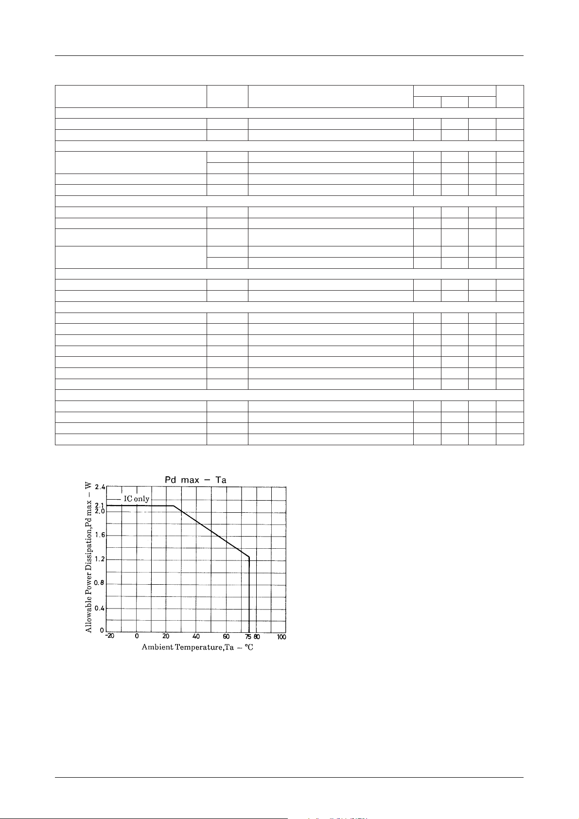
noitapissidrewopelbawollAxamdP 1.2W
erutarepmetgnitarepOrpoT 57+ot02–
erutarepmetegarotSgtsT 521+ot55–
V
V
1xam 02V
CC
2xam 0.7V
CC
W.V.TUO
TUO
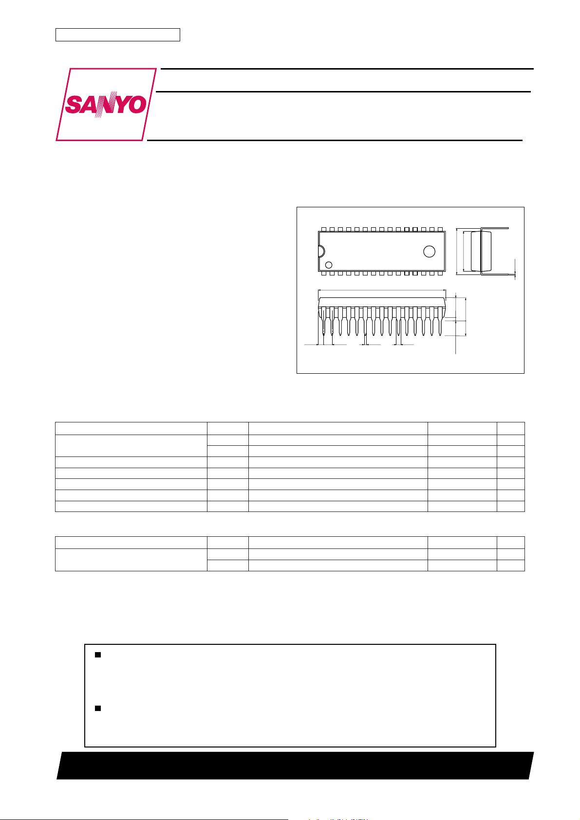
Package Dimensions
unit:mm
3061-DIP30S
[LB1687]
27.2
0.48 0.95
1.15
30
1
1.78
16
8.6
10.16
15
4.25
4.95max
3.2
0.51min
SANYO : DIP30S
0.25
22V
5.1A
˚C
˚C
Allowable Operating Ranges at Ta = 25˚C
retemaraPlobmySsnoitidnoCsgnitaRtinU
egatlovylppuS
VCC1 81ot5V
VCC2 5.6ot3.4V
22801TN (KT)/3260TA, TS No.3345–1/4
Page 2
LB1687
Electrical Characteristics at Ta = 25˚C, VCC1=12V, VCC2=5V
retemaraPlobmySsnoitidnoC
]ylppusrewoP[
1tnerrucylppuSI
2tnerrucylppuSI
]tuptuO[
egatlovnoitarutastuptuO
egatlovSRTtuptuOV
egatlovtnecseiuqtuptuOV
]tuptuo-tupnillaH[
egatlovtesffotupnireifilpmallaHV
tnerrucsaibtupnireifilpmallaHI
egatlovtupniedom-nommocreifilpmallaH
egnar
niagegatlovtuptuo-tupnillaH
]tuptuo-lortnoC[
niagevirdtuptuo-lortnoCG
ecnereffidHCtuptuo-lortnoC
]reifilpmaGF[
egatlovtesffotupnireifilpmaGFtesffoGFV 8–8+Vm
niagegatlovpool-nepOG
egatlovnoitarutastuptuoecruoSV
egatlovnoitarutastuptuokniSV
oitarnoitcejerlangisedom-nommoCRHC).etoneeS(08Bd
egnaregatlovtupniedom-nommocreifilpmaGFV
nigramesahP ).etoneeS(02.ged
]noitcetedrotoM[
htdiwsiseretsyhreifilpmanoitcetedrotoM 530556Vm
egatlovdlohserhtnipRC .HGIHotWOLmorfsegnahcRCV53.25.256.2V
erutarepmetnwodtuhslamrehTT
siseretsyhnwodtuhslamrehT
Note : Values shown are design targets only. No measurements have been taken.
1VCR,0=L=∞ 7103Am
CC
2VC0=5.65.9Am
CC
V
1I
)tas(O
V
QO
H
H
VHhc3.17.3V
G
OHV
G
OHV
OCV
∆G
GFV
DS
∆T
DS
TUO
2I
)tas(O
TUO
I
)sus(O
TUO
VC0=8.51.64.6V
tesffo5–5+Vm
saib 15Aµ
1 65Bd
2 34Bd
OCV
zHk1=f06Bd
IOAm2=7.3V
UOGF
I
DOGF
HCGF
Am2–= 3.1V
O
).etoneeS(051081012
).etoneeS(51
sgnitaR
nimpytxam
ecruos+knis,A5.0=6.12.2V
ecruos+knis,A0.1=0.20.3V
).etoneeS(Am02=02V
831444Bd
2–2+Bd
05.3V
tinU
˚C
˚C
No.3345–2/4
Page 3

Pin Assignment
Equivalent Circuit Block Diagram
LB1687
No.3345–3/4
Page 4

Truth Table
ecruoS
1
2
3
4
5
6
esahpV → esahpWH
esahpW → esahpU
esahpU → esahpWH
esahpV → esahpW
esahpW → esahpVH
esahpU → esahpV
esahpV → esahpUH
esahpV → esahpU
esahpU → esahpVH
esahpU → esahpW
esahpW → esahpUH
esahpW → esahpV
UVW
knis
HHL
HLL
LLH
LHL
HLH
LHH
LB1687
tupnI
CR/F
L
L
L
L
L
L
lortnoCesreveR/drawroF
Input :
H : High level. One of the inputs should hav e a potential at least
0.2V higher than the other.
L : Low level. One of the inputs should ha ve a potential at least
0.2V lower than the other.
Forward/reverse control :
H : 2.0 to VCC2
L : 0 to 0.3V
Specifications of any and all SANYO products described or contained herein stipulate the performance,
characteristics, and functions of the described products in the independent state, and are not guarantees
of the performance, characteristics, and functions of the described products as mounted in the customer's
products or equipment. To verify symptoms and states that cannot be evaluated in an independent device,
the customer should always evaluate and test devices mounted in the customer's products or equipment.
SANYO Electric Co., Ltd. strives to supply high-quality high-reliability products. However, any and all
semiconductor products fail with some probability. It is possible that these probabilistic failures could
give rise to accidents or events that could endanger human lives, that could give rise to smoke or fire,
or that could cause damage to other property. When designing equipment, adopt safety measures so
that these kinds of accidents or events cannot occur. Such measures include but are not limited to protective
circuits and error prevention circuits for safe design, redundant design, and structural design.
In the event that any or all SANYO products(including technical data,services) described or
contained herein are controlled under any of applicable local export control laws and regulations,
such products must not be exported without obtaining the export license from the authorities
concerned in accordance with the above law.
No part of this publication may be reproduced or transmitted in any form or by any means, electronic or
mechanical, including photocopying and recording, or any information storage or retrieval system,
or otherwise, without the prior written permission of SANYO Electric Co. , Ltd.
Any and all information described or contained herein are subject to change without notice due to
product/technology improvement, etc. When designing equipment, refer to the "Delivery Specification"
for the SANYO product that you intend to use.
Information (including circuit diagrams and circuit parameters) herein is for example only ; it is not
guaranteed for volume production. SANYO believes information herein is accurate and reliable, but
no guarantees are made or implied regarding its use or any infringements of intellectual property rights
or other rights of third parties.
This catalog provides information as of February, 2001. Specifications and information herein are subject
to change without notice.
PS No.3345–4/4
 Loading...